See discussions, stats, and author profiles for this publication at: https://www.researchgate.net/publication/322769247
Nanofabrication Process by Reactive Ion Etching of Polystyrene Nanosphere on Silicon Surface Research · January 2018 DOI: 10.13140/RG.2.2.17837.79842
CITATIONS
READS
0
103
6 authors, including: Jibrin Yabagi
Isah Mohammed Kimpa
Ibrahim Badamasi Babangida University
Federal University of Technology Minna
17 PUBLICATIONS 6 CITATIONS
19 PUBLICATIONS 44 CITATIONS
SEE PROFILE
SEE PROFILE
Zaidi Embong
Mohd Arif Agam
Universiti Tun Hussein Onn Malaysia
Universiti Tun Hussein Onn Malaysia
70 PUBLICATIONS 91 CITATIONS
39 PUBLICATIONS 39 CITATIONS
SEE PROFILE
SEE PROFILE
Some of the authors of this publication are also working on these related projects: ENERGY GAP INVESTIGATION AND CHARACTERIZATION OF KESTERITE CU 2 ZNSNS 4 THIN FILM FOR SOLAR CELL APPLICATIONS View project Desulfurization of diesel fuel View project
All content following this page was uploaded by Jibrin Yabagi on 29 January 2018. The user has requested enhancement of the downloaded file.
Journal of Science and Technology, Vol. 9 No. 3 (2017) p. 145-153
Nanofabrication Process by Reactive Ion Etching of Polystyrene Nanosphere on Silicon Surface Jibrin Alhaji Yabagi,1,2*, Mohammed Isah Kimpa1,3, Muhammad Nmaya Muhammad1,2, Nafarizal Nayan4, Zaidi Embong1 and Mohd Arif Agam1* 1*
4
Department of Physics and Chemistry, Universiti Tun Hussein Onn Malaysia, Pagoh Educational Hub, Johor Malaysia 2* Department of Physics, Ibrahim Badamasi Babangida University Niger State Nigeria 3 Department of Physics, Federal University of Technology Minna Niger State Nigeria Research Centre Microelectronic and Nanotechnology–Shamsuddin Universiti Tun Hussein Onn Malaysia 86400Parit Raja, Batu Pahat, Johor Malaysia.
Received 30 September 2017; accepted 30 November 2017; available online 28 December 2017 Abstract: Nanospheres made of organic polymer have been applied to generate various patterning mask in fabricating functional nanostructures. The patterning and generation of semiconductor nanostructures through nanospheres mask provides a potential alternative to the conventional top-down fabrication techniques. Polystyrene nanosphere was modified using reactive ion etching (RIE) with O2 plasma at various duration of exposure (0, 20, 40 sec) and further extended to produce nanostructure by employing combination of O 2 and mixed CHF3/SF6 gases. These edge PS nanospheres are later reduced as nanostructures and characterized using various characterization techniques such as Field Emission Scan Electron Microscopy/Energy Dispersive X-ray Spectroscopy (FESEM)/EDS, Atomic Force Microscopy and Fourier Transformation Infrared Spectroscopy (FTIR). The potential for multi stages etching procedures of O2 and later with SF6/CHF3 plasma etching are found to modify the nanospheres shapes and sizes which are important either as secondary mask for metal evaporation or as direct patterning of carbonaceous materials when exposed to irradiation sources. The nanostructures made using RIE will have applications in low power high performance electronic devices, optoelectronic, photovoltaic, biosensors and lithium ion battery devices. Keywords: Polystyrene; Nanostructure; RIE; O2 gas; SF6 gas; CHF3 gas.
1.
Introduction
Nanostructured materials have attracted a lot of attention these days because of their new electric, magnetic, optical [1], [2] or biological characteristics which are not obtainable with conventional non-structured materials. The applications range over many areas of science and technology, such as low dimensional electronic and magnetic systems, photo detectors, photo emitters, enhanced Raman scattering, filtration, bioreactors, biosensors, and high-density magnetic recording [3]–[5]. Polymers play an important role in nanofabrication of materials either as mask for lithography or its own unique properties, owing to it repetitive molecular unit, simple processabilty, low cost tunable properties and diverse functionalities [2],[6]–[10]. Polystyrene (PS) is one of the important polymers that exhibits many good properties, *Corresponding author:
[email protected] 2017 UTHM Publisher. All right reserved. penerbit.uthm.edu.my/ojs/index.php/jst
such as easy process, rigidity, low water absorbability, transparency, and that it can be produced at low cost [11]–[13]. The PS films have wide applications and are mainly employed in surface protection of metals, optical biosensor and humidity sensor, coatings for biomaterials and barrier films for pharmaceutical packaging. Many methods have been used in modify PS nanospheres shapes and sizes, such as reactive ion etching [2], [14], laser irradiation [12], [15], x-ray lithography, electron beam, ion beam and annealing [16]. One of the most popular methods for fabrication of nanomaterials is Reactive ion etching (RIE). It can also be used to modify PS nanospheres mask to create secondary lithography mask but it is also suitable to control the surface morphology and roughness of PS nanospheres especially in investigating surface hydrophobic and hydrophilicity of polymers for application as in electronics and biological applications [2]. The used of PS nanospheres
Journal of Science and Technology, Vol. 9 No. 3 (2017) p. 145-153
as mask and fabricating arrays of nanostructure materials through the aid of selfassembly of polystyrene nanospheres is called Nanospheres Lithography (NSL) technique, where the mask created can be varied through the single or multi-layer for metal evaporator mask. The arrays of metal nanostructures deposited through voids of PS nanospheres are dictated by the sizes used as mask and also by combining with other techniques such as RIE, secondary phase of lithography mask are able to be created. In the conventional NSL method, the nanostructure size can be controlled by the diameter of nanospheres used [17]. The array pitch is determined by the size; however, the nanostructure size can be arbitrarily selected by subsequent dry etching of the PS nanospheres. The ability to control size is important for obtaining a profound understanding the properties of nanostructured material and for improving characteristics in terms of technological applications [18]. Many studies have been reported for fabrication of nanostructure using PS spheres for examples He et al [19] fabricated vertical nanostructure arrays (VNAs) by plasma etching processes and their applications in biology, energy and electronics. Evtimova et al., [20] fabricated one-dimensional diamond nanostructures using nanocrystalline diamond films (NCD) as a starting material, where fabrication processed through electron beam lithography (EBL) and reactive ion etching in inductively coupled O2 plasma (ICP-RIE) was used to increased precise patterning of the diamond nanostructures. Wang et al., [21] reported facile and fast nano-fabrication technique for creating nanostructures based on combining the nanoimprint lithography (NIL) and nanosphere lithography (NSL) techniques, where monolayer self-assembled polystyrene colloidal particle as a mask for dry etching of SiO2 to create periodic ordered nano-plates on glass substrates. In this article, approach of producing nanostructure using reactive ion etching (RIE) with three different gases: pure O2 and mixture CHF3/SF6 consist of 3 stages, first stage; coating method using PS nanospheres to form hexagonal close-packed single or double layers. Second stage, reducing the size and separation of the PS spheres by reactive ion etching with O2 plasma etching for different etching duration (20 and 40 s). Third stage,
using couple capacitive plasma (CCP) with mixture of CHF3 and SF6 to etch the PS films with the following conditions: CHF3 flow 80 sccm, SF6 flow 40 sccm, RF power 50 W for 20 and 40 s. Investigations of treated and untreated were analyzed using field emission scan microscopy (FE-SEM), Energy dispersive spectroscopy (EDS), atomic force microscopy (AFM) and Fourier Transformation Infrared (FTIR).
2.
Experimental Details
Polystyrene (PS) nanospheres with the diameter of 500 nm were drop-coated onto silicon wafer with the following procedure: in order to obtain a monolayer of PS nanospheres, the silicon wafer p-type with orientation (100) surface was made hydrophilic by immersion in a piranha solution of 3:1 concentrated H2SO4/H2O2 at 80 ºC for 40 min, rinsed thoroughly with ultra-pure water and dried in a stream of nitrogen, thus created hydrophilic surfaces. The PS nanosphere solution was diluted in deionized water then coated on the substrate surface with the volume-controlled pipette. Finally, the PS monolayer was uniformly distributed within the area of 1x1 cm2. Reactive ion etching (RIE) (SnTEK Technology) with couple capacitive plasma (CCP) was used, where nanostructures were made by two stages of etching process. PS was etching with O2 plasma at flow rate 50 sccm, pressure 200 m Torr and 50 W RF power. This procedures were taken to tailor the size and separation of the PS nanospheres by adjusting the etching duration for 20 and 40 s. Afterward, a mixture of CHF3/SF6 with ratio of 2:1 sccm 80/40 sccm plasmas at the fixed chamber pressure (200 mTorr) and RF power (50 W) was employed with the etching durations of 20 and 40 s respectively. Morphologies and elemental composition of the samples were observed using field emission scanning electron microscopy (FE-SEM, JEOL JSM-6500) and the energy dispersive spectroscopy (EDS) and coated with platinum before characterization. Topography and roughness of the samples were studied using atomic force microscopy (AFM) XE-100 Park systems. The measurement was carried out using noncontact mode under the room temperature 146
Journal of Science and Technology, Vol. 9 No. 3 (2017) p. 145-153
conditions with scan size of 5 μm x 5 μm, high resolution 256 pixels x 256 pixels. FTIR analysis was performed using a Perkin Elmer FTIR Spectrometer LR 64912C N3896 equipped with a universal Attenuated Total Reflectance (ATR) sample stage. The sample molecular structure was determined within the range of 4000–400 cm−1 with a resolution of 4 cm−1. 3. 3.1
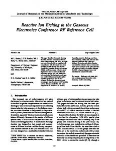
Fig. 1(b-c). Since the position of each PS nanospheres remain the same after the oxygen RIE, the separations between each PS nanospheres increased as the sizes of nanospheres decreased. Though, the etching process caused a minor increase in surface roughness on the etched beads that is in general PS nanospheres were etched evenly in the lateral dimension within the duration of 20 and 40 s. The heights of nanospheres were decreased gradually during the RIE process. Fig. 1 (e-f) corresponds to images of PS nanospheres etched with CHF3/SF6 gas mixtures. The Si substrates are believed to be etched too as the mixture of CHF3/SF6 are commonly used to gives highly anisotropic Si etching. This is due to the fact that with the addition of CHF3 to SF6 gas, CF2 radicals are produced as blocking layer on the Si sidewalls during etching. The differences of etching rate PS nanospheres and Si, where the higher etching rate of CHF3/SF6 compared with O2 plasma etching and the isotropic nature of process in the case of O2 gas could be further used to fabricate nanostructures such as nanopillars, nanotriangulars and nanorings.
Results and Discussion Morphological Analysis
Fig. 1 (a-f) show analysis of SEM images obtained for untreated and treated polystyrene. Fig. 1(a) shows the morphology of the untreated PS nanospheres. At initial states, the self-assembled monolayers of PS are found to form in hexagonal close-packed arrangement on the silicon substrate. Treated PS for the first RIE stage, using O2 gas plasma etching process, average diameter of the individual PS nanospheres are found to be reduced in sizes and shapes. The PS nanospheres average diameter reduction through O2 gas plasma etching process are found to corresponded linearly with etching duration as can be seen in 0s
20 s
0s (d)
40 s
(b)
(a)
(c)
20 s CHF3/SF6 (e)
40 s CHF3/SF6 (f)
Fig. 1: FESEM images of untreated and treated PS with O2 plasma (a) 0 s, (b) 20 s (c) 30 s and mixture of CHF3/SF6 (d) 0 s, (e) 20 s, (f) 40 s
3.2
Elemental Composition Analysis
Elemental composition analysis was carried out using EDS (Energy Dispersive
Spectroscopy) to determine the weight and atomic percentage of carbon and silicon present for untreated and treated O2 plasma etching. Results are summarized in Table 1; 147
Journal of Science and Technology, Vol. 9 No. 3 (2017) p. 145-153
The PS nanospheres show 81.52 % by weight & 91.16 % for carbon and silicon element before any plasma treatment. The treated PS with 20 and 40 s of O2 plasma etching were found to reduce in weight and atomic %, reduction of carbon, silicon are 74.06% & 0s
86.97% and 51.35% & 71.17% respectively. Fig. 2 (a-c) shows the EDS spectrum for carbon and silicon, where reduction of carbon materials are obvious in the EDS spectrum of 40 s compared to 20 s. 20 s
(b)
(a)
40 s (c)
Fig. 2: EDS spectra of untreated and treated PS with O2 plasma etching (a) 0, (b) 20 and (c) 40 s Table 1 Elemental composition of PS treated with O2 plasma etching. Sample PS PS RIE 20 sec PS RIE 40 sec
3.3
Element CK Si K CK Si K CK Si K
Weight % 81.52 18.48 74.06 25.94 51.35 48.65
Atomic % 91.16 8.84 86.97 13.03 71.17 28.83
Atomic Force Microscopy Analysis
Atomic force microscopy is a powerful tool for topography study of the films and obtain information about the roughness, height asymmetries values such as the skewness and kurtosis of the films [22]. The average roughness, root mean square (rms) and height asymmetry values are measured using a software analysis from AFM instrument and the results obtained are summarized Table 2.
Fig. 3 (a-c) appears to have gradual changes the PS nanospheres where average roughness of samples decreases as the etching time increases. Fig. 4(a-c) shows the AFM images obtained both for untreated and treated polystyrene with RIE. Fig. 4a show that for untreated PS with many sharp and regular present over the whole substrate surface. The surface roughness decreased after treating PS with O2 plasma and CHF3/SF6 gas compared to untreated PS. This could be caused by highly energetic ions and radicals of plasma, because exposure to the active residuals and ions of plasma could result in dissociation of some chemical bonds from the surface of polymers which results in changing morphology of the samples [5].
148
Journal of Science and Technology, Vol. 9 No. 3 (2017) p. 145-153
(a) 0 s
(b) 20 s O2
(c) 40 s O2
Fig. 3: Topography images of pre and post RIE treatment of PS during O2 plasma for (a) 0, (b) 20 and (c) 40 s. (a) 0 s CHF3/SF6
(b) 20 s CHF3/SF6
(c) 40 s CHF3/SF6
Fig. 4: Topography images of pre and post RIE treatment for PS with CHF3/SF6 for (a) 0, (b) 20 and (c) 40 s. Table 2 AFM Statistical parameters of the O2 plasma and CHF3/SF6 RIE polystyrene thin films at different duration Statistical parameters Average roughness (nm) RMS roughness (nm) Skewness Ssk Kurtosis Sku
Pure PS 20.4 23.8 0.29 2.39
Samples O2 RIE 20 sec 40 sec 54.2 38.2 67.0 46.3 0.81 0.08 3.59 2.50
CHF3/SF6 20 sec 40 sec 21.3 19.7 26.8 16.3 0.27 0.21 2.99 2.56
149
Journal of Science and Technology, Vol. 9 No. 3 (2017) p. 145-153
3.4
Fourier transformation infrared (FTIR) analysis
RIE surface modifications of polystyrene nanosphere are confirmed by Fourier transformation infrared. FTIR spectroscopy in attenuated total reflection (ATR) mode is one of the methods used to bring out the finer surface information. This technique was used to characterize the polymer surface. The spectra of the treated and untreated samples are compared to observe the changes. Fig. 5(ac) shows the ATR-FTIR spectra of untreated polystyrene and treated with oxygen plasma. Fig. 5a show the characteristic bands at 3023 cm−1, 1601 cm−1, 1490 cm−1, 1447 cm−1 and 902 cm−1 correspond to the phenyl group, the peaks at 2924 cm−1 and 2846 cm−1 are assigned to the methylene and methenyl groups, the peak at 1023 cm−1 is correspond to the C–O bond [15], [23]. When untreated polystyrene spectrum is compared with the oxygen-treated polystyrene spectrum, it is seen that broad band occurs around 3698 cm−1 and
2970 cm−1, which led to formation of oxygenbased functional group on the surface due to collision of the radicals components of oxygen to the polystyrene surface [24]–[28]. Etching of the polymer surface through the reaction of atomic oxygen with the surface carbon atom, giving volatile reaction products and other one is the formation of oxygen functional groups at the polymer surface through the interaction between the active species from the plasma and the surface atom [18],[22], [23]. Fig. 6(ac) shows the spectra of PS treated and untreated with mixture of CHF3/SF6 gases. Treated PS with CHF3/SF6 bands are found to be affected, bands reduced some intensity and become broader compared with O2 plasma treated and untreated PS which indicates the structural changes as a result of CHF3/SF6. It’s clearly show that new peak appear at 1207 cm−1 for 20 s, intensities of band at 1601 cm−1, 1490 cm−1, 1447 cm−1, 1023 cm-1 disappear after 40 s and created new peaks at 3863 cm−1, 3674 cm−1, 2275 cm−1 due to CHF3/SF6.
Fig. 5: FTIR spectra of untreated and treated PS with O2 plasma etching for (a) 0, (b) 20 and (c) 40 s.
150
Journal of Science and Technology, Vol. 9 No. 3 (2017) p. 145-153
Fig. 6: FTIR spectra of untreated and treated PS with mixture of CHF3/SF6 gases for (a) 0, (b) 20 and (c) 40 s.
4.
Conclusion
In conclusion, polystyrene nanosphere was successfully prepared by drop coating method onto substrate and developed a low cost with high throughput fabrication process for nanostructures with modification of the PS nanosphere by plasma treatment and RIE at different etching time. The size and separation of the fabricated nanostructures can be independently adjusted by selecting different etching time and by using an optimum plasma modification process. Also, the new modified fabrication of nanostructures can lead to new applications in electronics, optoelectronics and biosensor devices.
Shamsuddin Research Centre (MiNT-SRC) and Centre for Graduate Studies Universiti Tun Hussein Onn Malaysia. References [1]
[2]
[3] Acknowledgements This work was financially supported by Graduate Research Incentive Grant (GIPS) Project Vot U302 Faculty of Applied Sciences and Technology Universiti Tun Hussein Onn Malaysia and Ibrahim Badamasi Babangida University Lapai. Authors are also gratefully acknowledge the continued support from Microelectronics and Nanotechnology
[4]
Choi, D. G., Yu, H. K., Jang, S. G., & Yang, S. M. (2004). “Colloidal lithographic nanopatterning via reactive ion etching” Journal of the American Chemical Society, 126, 7019–7025 Acikgoz, C., Hempenius, M. A., Huskens, J., & Vancso, G. J. (2011). “Polymers in conventional and alternative lithography for the fabrication of nanostructures” European Polymer Journal, 47, 2033–2052. Loeschner, K., Seifert, G., & Heilmann, A. (2010). “Self-organized, gratinglike nanostructures in polymer films with embedded metal nanoparticles induced by femtosecond laser irradiation” Journal of Applied Physics, 108. doi:10.1063/1.3490191 Wei, X., Chen, X., & Jiang, K. (2011). “Fabrication of Nickel Nanostructure Arrays Via a Modified Nanosphere Lithography Nanoscale Research 151
Journal of Science and Technology, Vol. 9 No. 3 (2017) p. 145-153
[5]
[6]
[7]
[8]
[9]
[10]
[11]
[12]
[13]
[14]
Letters, 6, 1–5. Mirzadeh, H., & Bagheri, S. (2007). “Comparison of the effect of excimer laser irradiation and RF plasma treatment on polystyrene surface” Radiation Physics and Chemistry, 76, 1435–1440 Lyuksyutov, S. F., Vaia, R. a, Paramonov, P. B., Juhl, S., Waterhouse, L., Ralich, R. M., Sancaktar, E. (2003). “Electrostatic nanolithography in polymers using atomic force microscopy” Nature Materials, 2, 468– 472. Meena, J. S., Chu, M., Singh, R., Wu, C., Chand, U., You, H.-C., Ko, F.-H. (2014).“Polystyrene-block poly(methylmethacrylate) composite material film as a gate dielectric for plastic thin-film transistor applications” RSC Advances, 4, 18493. Yang, T. I., & Kofinas, P. (2007). “Dielectric properties of polymer nanoparticle composites” Polymer, 48, 791–798. Pfleging, W., Kohler, R., Schierjott, P., & Hoffmann, W. (2009). Laser patterning and packaging of CCD-CEChips made of PMMA” Sensors and Actuators, B: Chemical, 138, 336–343. Li, H., & Huck, W. T. S. (2002). Polymers in nanotechnology. Current Opinion in Solid State and Materials Science (Vol. 6). Riedel, D., Wehlus, T., Reusch, T. C. G., & Brabec, C. J. (2016). “Polymerbased scattering layers for internal light extraction from organic light emitting diodes” Organic Electronics, 32, 27–33. Fan, W., Zhang, C., Tjiu, W. W., & Liu, T. (2013). “Fabrication of electrically conductive graphene/polystyrene composites via a combination of latex and layer-by-layer assembly approaches” Journal of Materials Research, 28, 611–619. Xiao, T., Cai, C., Peng, L., & Wu, W. (2013). “Fabrication and characteristics of self-assembly nano-polystyrene films by laser induced CVD” Applied Surface Science, 282, 652–655. Chen, H., Wang, T., Shen, H., Liu, W., Wang, S., Liu, K., Yang, B. (2015). “Ag
[15]
[16]
[17]
[18]
[19]
[20]
[21]
[22]
nanoparticle/polymer composite barcode nanorods” Nano Research, 8, 2871–2880 Yabagi, J. A., Kimpa, M. I., Muhammad, M. N., Uthaman, K. I., Zaidi, E., & Agam, M. A. (2017). “Structural transformation of polystyrene nanosphere produce positive and negative resists by controlled laser exposure” Advanced Science Letters, 23, 6613–6617 Mustafa, M. U., Agam, M. A., Md Juremi, N. R., Mohamad, F., Wibawa, P. J., & Ali, A. H. (2011). “Physical and chemical changes of polystyrene nanospheres irradiated with laser” AIP Conference Proceedings, 1347, 67–71. Guruvenket, S., Rao, G. M., Komath, M., & Raichur, A. M. (2004). “Plasma surface modification of polystyrene and polyethylene” Applied Surface Science, 236, 278–284 Espejo, C., Carrión-Vilches, F. J., & Bermúdez, M. D. (2014). “Effect of the nature of the carbon nanotubes and modification by ionic liquid” Polymer Degradation and Stability, 103, 42–48 He, B., Yang, Y., Yuen, M. F., Chen, X. F., Lee, C. S., & Zhang, W. J. (2013). “Vertical nanostructure arrays by plasma etching for applications in biology, energy, and electronics” Nano Today, 8, 265–289 Evtimova, J., Kulisch, W., Petkov, C., Petkov, E., Schnabel, F., Reithmaier, J. P., & Popov, C. (2013). “Reactive ion etching of nanocrystalline diamond for the fabrication of one-dimensional nanopillars” Diamond and Related Materials, 36, 58–63 Wang, B., Zhao, W., Chen, A., & Chua, S.-J. (2006). “Formation of nanoimprinting mould through use of nanosphere lithography” Journal of Crystal Growth, 288, 200–204 Gulen, M., Yildirim, G., Bal, S., Varilci, A., Belenli, I., & Oz, M. (2013). “Role of annealing temperature on microstructural and electro-optical properties of ITO films produced by sputtering” Journal of Materials Science: Materials in Electronics, 24, 467–474. 152
Journal of Science and Technology, Vol. 9 No. 3 (2017) p. 145-153
[23] Wibawa, P. J., Agam, M. A., Nur, H., & Saim, H. (2011). “Changes in physical properties and molecular structure of polystyrene nanospheres exposed with solar flux” AIP Conference Proceedings, 1341, 54–61. [24] Jäger, M., Sonntag, F., Pietzsch, M., Poll, R., & Rabenau, M. (2007). “Surface modification of polymers by using excimer laser for biomedical applications” Plasma Processes and Polymers, 4, 416–418. [25] Guo, B., Li, S., Song, L., Yang, M., Zhou, W., Tyagi, D., & Zhu, J. (2015). “Plasma-treated polystyrene film that enhances binding efficiency for sensitive and label-free protein biosensing” Applied Surface Science, 345, 379–386. [26] Koval, Y. (2004). Mechanism of etching and surface relief development of PMMA under low-energy ion bombardment” Journal of Vacuum Science & Technology B: Microelectronics and Nanometer Structures, 22, 843. [27] Nakayama, Y., Takahagi, T., Soeda, F., Hatada, K., Nagaoka, S., Suzuki, J., & Ishitani, A. (1988). “XPS analysis of NH3 plasma-treated polystyrene films utilizing gas phase chemical modification” Journal of Polymer Science Part A: Polymer Chemistry, 26, 559–572. [28] Alsharaeh, E. H. (2016). “Polystyrenepoly(methyl methacrylate) silver nanocomposites: Significant modification of the thermal and electrical properties by microwave irradiation” in Materials, 9. [29] Guruvenket, S., Rao, G. M., Komath, M., & Raichur, A. M. (2004). “Plasma surface modification of polystyrene and polyethylene” in Applied Surface Science, 236, 278–284. [30] Fernández-Sánchez, C., Pellicer, E., Orozco, J., Jiménez-Jorquera, C., Lechuga, L. M., & Mendoza, E. (2009). “Plasma-activated multi-walled carbon nanotube-polystyrene composite substrates for biosensing” in Nanotechnology, 20, 335501.
153
View publication stats