APPLIED PHYSICS LETTERS 97, 023511 共2010兲
Nonvolatile organic transistor-memory devices using various thicknesses of silver nanoparticle layers S. M. Wang,1,2 C. W. Leung,1 and P. K. L. Chan2,a兲 1
Department of Applied Physics, The Hong Kong Polytechnic University, Kowloon, Hong Kong Department of Mechanical Engineering, The Hong Kong Polytechnic University, Kowloon, Hong Kong
2
共Received 19 May 2010; accepted 18 June 2010; published online 15 July 2010兲 We demonstrate the modification of the memory effect in organic memory devices by adjusting the thickness of silver nanoparticles 共NPs兲 layer embedded into the organic semiconductor. The memory window widens with increasing Ag NPs layer thickness, a maximum window of 90 V is achieved for 5 nm Ag NPs and the on/off current ratio decreases from 105 to 10 when the Ag NPs layer thickness increases from 1 to 10 nm. We also compare the charge retention properties of the devices with different Ag NPs thicknesses. Our investigation presents a direct approach to optimize the performance of organic memory with the current structure. © 2010 American Institute of Physics. 关doi:10.1063/1.3462949兴 The advent of the nonvolatile flash memory has provided remarkable benefits for data storage in computers and other portable electronic devices. Due to the advantages of organic electronic devices over their inorganic counterparts such as the low fabrication costs, suitable for large area fabrication, and compatible with flexible substrates,1,2 organic memory devices fabricated on flexible substrates have great potential for the next generation of nonvolatile flash memory. They can be further integrated with other electronic devices and form a flexible circuit. Recently a 26⫻ 26 array of organic flash memory transistors based on floating gate structure was demonstrated on flexible plastic sheets, and the operating voltage was as low as 6 V.3 Currently, different approaches have been adopted to fabricate organic nonvolatile memory devices, such as using ferroelectric polymer dielectric materials4,5 and chargeable gate dielectric in the organic field-effect transistors 共OFETs兲.6 In these devices, the memory effect arises from the field effect modulation by either the spontaneous polarization that occurs in ferroelectric, or through the trapping of charges in a chargeable layer of the dielectric.7 Usually, the charge-trapping elements in the chargeable gate dielectric are nanoparticles 共NPs兲 of metals such as Cr,8 Au,6 and Ag.9 Compared with ferroelectric polymer-based memory, devices using metal NPs as charge traps have an advantage that the trap density and distribution can be controlled by adjusting the density and location of the NPs during the NP formation process, by using ultrathin metallic films deposition or ion implantation techniques.10,11 Recently, we reported a different structure of transistor memory device with remarkable memory window performance by placing silver NPs in between two pentacene layers.12 A significant advantage of the structure is that it can eliminate the extra fabrication steps for the insulator layers as in the case of floating gate transistor memory structure, making it suitable for integrating with other electronic devices on the same substrate to form a circuit. In the current work, we focused on investigating the performance variation in the pentacene OFET-based memory with different silver NP layer thickness. We also compared the memory window, Author to whom correspondence should be addressed. Tel.: ⫹852 27666664. Electronic mail:
[email protected].
a兲
0003-6951/2010/97共2兲/023511/3/$30.00
on/off current ratio, and charge retention properties of the devices. The experimental results suggest a guideline for optimizing the thicknesses of the NP layer in the device for different application criteria. The bottom-gate transistor memory devices were fabricated on highly doped n-type Si substrates with 300 nm SiO2, and the device configuration was in the form of pentacene/Ag NPs/pentacene 关schematic diagram shown in Fig. 2共a兲兴. Pentacene thin films and silver NPs were thermally evaporated at a base pressure of 1 ⫻ 10−7 Torr. The thickness of the first and second pentacene layers were 15 nm and 25 nm, respectively. The Ag layer varied with a nominal thickness of 1, 5, and 10 nm, and the corresponding devices were named as devices A1, A5, and A10. The 50 nm thick silver source and drain electrodes were patterned by shadow mask, and the channel lengths 共L兲 and widths 共W兲 were 50 m and 1000 m, respectively. The output and double-sweep transfer characteristics of the transistors were measured by two Keithley 2400 sourcemeters. All the measurements were performed in dark and ambient conditions, immediately after the devices were taken out of the thermal evaporation chamber. The output characteristics for devices A1, A5, and A10 are shown in Figs. 1共a兲–1共c兲. The gate voltage 共Vg兲 was varied from 0 to ⫺60 V with a 10 V step. It can be noticed that for devices A1 and A5, the output curves exhibit a typical p-channel field-effect transistor behavior, with the hole accumulation mode at negative Vg and hole depletion mode at positive Vg. The calculated carrier mobility in the saturation region is about 0.34 cm2 V−1 s−1 for device A1, three times larger than that of device A5 共0.10 cm2 V−1 s−1兲. However, device A10 does not show obvious saturation in the output curves and the drain source current is large 共about 2 ⫻ 10−6 A兲 even at a positive gate bias of 60 V, which suggests the off state of device A10 cannot be achieved. The hysteresis properties of these three devices were investigated by cyclic sweeping of Vg 共i.e., from positive to negative and then back to positive兲. The memory window of a device is defined as the difference of the threshold voltages in the two Vg sweeping directions, i.e., ⌬Vth = Vth1 − Vth2. As shown in Fig. 1共d兲, the memory window shows a remarkable
97, 023511-1
© 2010 American Institute of Physics
Downloaded 19 Dec 2010 to 158.132.161.9. Redistribution subject to AIP license or copyright; see http://apl.aip.org/about/rights_and_permissions
023511-2
Wang, Leung, and Chan
Appl. Phys. Lett. 97, 023511 共2010兲
FIG. 1. 共Color online兲 The output characteristics of the transistor memory with Ag NPs thickness of 共a兲 1 nm, 共b兲 5 nm, and 共c兲 10 nm. 共d兲 The transfer characteristics of the transistor memory with Ag NPs thickness 1–10 nm.
dependence on the silver NP layer thickness. When the Ag NPs thickness is 1 nm, the memory window is about 60 V, with a large on/off current ratio of 105. When the NP layer thickness increases to 5 nm, the memory windows increase to 90 V, and the on/off current ratio drops to 103 due to the larger off current. For the device with 10 nm thick Ag NPs, although the off state is difficult to be defined from the output characteristic curves, a significant memory window can still be observed in the transfer characteristic curve with a small on/off current ratio of 10. The decrease in on/off current ratio from device A1 to A10 is believed to be due to the gradual size increase and partially connected silver NPs, which are likely to create low resistance current paths and hence increases the off-current. As the physical origin of the memory effect in the devices is due to the thermal evaporated Ag atom diffusing and penetrating into the pentacene layer and forming dopant-like traps,13,14 the enhancement of the memory window is attrib-
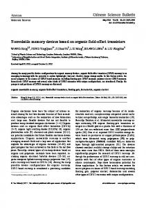
uted to the larger trap density induced by the NPs. Scanning electron microscopy 共SEM兲 images of Ag NPs on 15 nm pentacene layer are shown in Figs. 2共b兲–2共d兲. For 1 nm Ag NPs, the NPs cannot be clearly observed in the SEM image and it is possibly due to the resolution limit of the SEM. On the other hand, for 5 and 10 nm thick Ag layers deposited on pentacene, NPs with different size can be clearly observed as shown in Figs. 2共c兲 and 2共d兲. The areal densities of Ag NPs are evaluated by the image processing function in MATLAB as 3.3⫻ 1011 cm−2 and 1.9⫻ 1011 cm−2 in device A5 and A10, respectively, one order of magnitude higher than that of gold NPs formed on SiO2 insulating layer by solution immersion method 共2 – 5 ⫻ 1010 cm−2兲 with the memory window of 22 V.15 Practically, the large memory window and small on/off ratio of 103 of device A5 allow us to design devices with multilevel storage despite compromised on/off current ratio,16 while device A1 can satisfy applications which re-
FIG. 2. 共Color online兲 共a兲 The schematic structure of pentacene/Ag/ pentacene configuration devices; SEM images of Ag NPs on 15 nm bottom pentacene layer, the nominal thickness for Ag NPs are 共b兲 1 nm, 共c兲 5 nm, and 共d兲 10 nm.
Downloaded 19 Dec 2010 to 158.132.161.9. Redistribution subject to AIP license or copyright; see http://apl.aip.org/about/rights_and_permissions
023511-3
Appl. Phys. Lett. 97, 023511 共2010兲
Wang, Leung, and Chan
FIG. 3. 共Color online兲 Retention time measurement for devices A1 and A5.
quire a moderate memory window but a large on/off current ratio. Retention time of charge carriers is another important parameter for the operation of nonvolatile memory devices. Figure 3 shows the retention time of on- and off-currents of device A1 and A5. After applying a writing pulse of ⫺100 V 共erasing pulse of +100 V兲 with a pulse width of 5 s, we measured the off- 共on-兲 current with time intervals of 5 s at Vg = 0 V and Vds = −60 V. To eliminate the aging effect in ambient conditions and to ensure identical starting conditions, the samples were stored under vacuum for about 10 h after finishing the on-current measurement and before the off-current measurement was performed. The on-current of both devices show an obvious decay at initial stage and then keep constant for both devices. This initial decrease is related to the trap filling process by the applied drain source voltage as the traps are emptied after positive gate bias of 100 V. During the trap filling process, the number of free charge carriers decreases hence the on-current decreases. For device A5, the on-current decays faster than that of device A1 and it could be due to its larger trap density in device A5. The off-current, on the contrary, shows a remarkable difference for the two devices; in device A5, the off-current increases slowly during the whole measurement time of 12 h, demonstrating a long trap lifetime and a relatively stable charge retention behavior; the on/off current ratio decreases from 500 at the beginning to 3.5 after 12 h. However, in device A1, the off-current maintains constant at the first one hour then rises sharply by two orders of magnitude, indicating a poor charge retention capability of the trap states in this device. Thus, the initial high on/off current ratio of 104 decreased to 10 after 12 h. It is also important to notice that the off-current of device A1 is larger than A5 after 12 h of measurement. Such an increase in the off-current is related to the charges releasing process from the trap centers, and the difference in charge retention behavior may be ascribed to the difference trap states level in 1 and 5 nm Ag NPs. As discussed by other groups,17–19 the work function of metal increases with decreasing size of NPs, hence the 1 nm Ag NPs has a Fermi level closer to highest occupied molecular orbital level of pentacene while comparing with the 5 nm Ag NPs. As a result the shallower trapped charges in device A1 were released more easily from the trap centers and resulting in a fast increase in the off-current in the retention time mea-
surement. On the contrast, the deeper traps level in 5 nm Ag NPs device are beneficial for the stored charges, therefore reducing the charges loss rate and enhancing the charge retention property. Similar mechanism has been observed in silicon based metal-oxide-semiconductor memory where deep traps density in the floating gate governs the charge retention of the device.20–22 In conclusion, OFET-based memory devices with different memory properties were demonstrated by controlling the Ag NPs layer thickness. The 1 nm Ag NP device shows a moderate memory window with 60 V and large on/off current ratio at about 105. The 5 nm device exhibits larger memory window of 90 V but the on/off current ratio decrease to 103. The charge retention behaviors of the devices were also studied and 5 nm Ag NP device show a longer retention time comparing with the 1 nm Ag NP device. The variation in the retention time is due to different trap states level similar to the silicon based memory device. Our finding suggests a way to optimize the organic memory performance for different application criteria. This work was supported by research grants 共Grant Nos. 1-ZV43, 1-ZV4H, and A-PJ73兲 from Hong Kong Polytechnic University. Funding from HKSAR through UGC grant 共Grant No. PolyU 5112/08E兲 is also acknowledged. C. D. Dimitrakopoulos and P. R. L. Malenfant, Adv. Mater. 共Weinheim, Ger.兲 14, 99 共2002兲. 2 W. Wang, J. Shi, and D. Ma, IEEE Trans. Electron Devices 56, 1036 共2009兲. 3 T. Sekitani, T. Yokota, U. Zschieschang, H. Klauk, S. Bauser, K. Takeuchi, M. Takamiya, T. Sakurai, and T. Someya, Science 326, 1516 共2009兲. 4 R. C. G. Naber, C. Tanase, P. W. M. Blom, G. H. Gelinck, A. W. Marsman, F. J. Touwslager, S. Setayesh, and D. M. De Leeuw, Nature Mater. 4, 243 共2005兲. 5 Y. J. Park, H. J. Jeong, J. Chang, S. J. Kang, and C. Park, J. Semicond. Technol. Sci. 8, 51 共2008兲. 6 W. L. Leong, P. S. Lee, A. Lohani, Y. M. Lam, T. P. Chen, S. Zhang, A. Dodabalapur, and S. G. Mhaisalkar, Adv. Mater. 共Weinheim, Ger.兲 20, 2325 共2008兲. 7 B. N. Pal, P. Trottman, J. Sun, and H. E. Katz, Adv. Funct. Mater. 18, 1832 共2008兲. 8 C. J. Kim, S. W. Ryu, Y. K. Choi, J. J. Chang, S. H. Bae, and B. H. Sohn, Appl. Phys. Lett. 93, 052106 共2008兲. 9 D. Gupta, M. Anand, S. W. Ryu, Y. K. Choi, and S. H. Yoo, Appl. Phys. Lett. 93, 224106 共2008兲. 10 J. S. Lee, J. H. Cho, C. Y. Lee, I. Kim, J. J. Park, Y.-M. Kim, H. Y. Shin, J. Lee, and F. Caruso, Nat. Nanotechnol. 2, 790 共2007兲. 11 Z. Liu, C. Lee, V. Narayanan, G. Pei, and E. C. Kan, IEEE Trans. Electron Devices 49, 1606 共2002兲. 12 S. M. Wang, C. W. Leung, and P. K. L. Chan, Org. Electron. 11, 990 共2010兲. 13 J. H. Cho, D. H. Kim, Y. Jang, W. H. Lee, K. Ihm, J. H. Han, S. Chung, and K. Cho, Appl. Phys. Lett. 89, 132101 共2006兲. 14 J. Lin and D. G. Ma, J. Appl. Phys. 103, 024507 共2008兲. 15 C. Novembre, D. Guérin, K. Lmimouni, C. Gamrat, and D. Vuillaume, Appl. Phys. Lett. 92, 103314 共2008兲. 16 H. K. Lau and C. W. Leung, J. Appl. Phys. 104, 123705 共2008兲. 17 K. Wong, S. Vongehr, and V. V. Kresin, Phys. Rev. B 67, 035406 共2003兲. 18 K. H. Meiwes-Broer, Hyperfine Interact. 89, 263 共1994兲. 19 N. S. Phala and E. Steen, Gold Bull. 40, 150 共2007兲. 20 Y. Shi, K. Saito, H. Ishikuro, and T. Hiramoto, J. Appl. Phys. 84, 2358 共1998兲. 21 H. C. You, T. H. Hsu, F. H. Ko, J. W. Huang, W. L. Yang, and T. F. Lei, IEEE Electron Device Lett. 27, 653 共2006兲. 22 M. C. Kim, S. Kim, S. H. Choi, K. Belay, R. G. Elliman, and S. P. Russo, IEEE Electron Device Lett. 30, 837 共2009兲. 1
Downloaded 19 Dec 2010 to 158.132.161.9. Redistribution subject to AIP license or copyright; see http://apl.aip.org/about/rights_and_permissions