Journal of the Korean Physical Society, Vol. 50, No. 1, January 2007, pp. 49∼52
Nonvolatile Memory Devices Fabricated by Using Colloidal Ni Nanocrystals Kwang Soo Seol,∗ Kyung Sang Cho, Byung-Ki Kim, Jae-Young Choi, Eun-Kyung Lee, Yo-Sep Min and Jong-Bong Park Samsung Advanced Institute of Technology, P. O. Box 111, Suwon 440-600
Suk-Ho Choi† Department of Physics and Applied Physics, College of Electronics and Information, Kyung Hee University, Yongin 449-701 (Received 17 October 2006) Single-layered Ni nanocrystals (NCs) with an areal density of 2 × 1011 cm−2 have been prepared on SiO2 /Si substrates by spin coating of a Ni NC colloidal solution and subsequent drying without any further heat treatment. The presence of isolated Ni NCs of ∼9 nm on SiO2 is confirmed by scanning and transmission electron microscopic images. Nonvolatile memory (NVM) metal-oxide-semiconductor capacitors with a structure of SiO2 /Ni NCs/SiO2 /Al2 O3 exhibit a relatively large memory window of 3 – 5 V for 10 ms – 1 s under ±19 V. The flat-band voltages show almost no significant degradation up to 104 program/erase cycles. These results show that Ni NCs can be utilized for NVM devices. PACS numbers: 73.63.Bd, 73.40.Qv, 85.35.Be, 81.07.Bc Keywords: Ni nanocrystals, Nonvolatile memory, Colloidal synthesis, Spin coating
ing gates by self-assembling of a wetting layer of metal (2 – 10 nm in thickness) [5,6]. However, it is difficult to control both the dot size and the areal density simultaneously by using the self-assembling method. In addition, the metal NCs formed by that method generally show a broad size distribution. A high areal density of metal NCs with uniform size distribution is crucial to embody an ideal metal NC memory [4]. A colloidal synthesis method has proven to be promising for fabricating metal NCs with a narrow size distribution below 10 nm [8,9]. It is also easy to coat singlelayered colloidal NCs on Si substrates by using a conventional spin-coating method [10] without any further heat treatment, which should give a great advantage to metal NC memories. In this paper, we report Ni NC memories, where the Ni NCs as floating gates were formed by using a colloidal synthesis method.
I. INTRODUCTION Nanocrystal (NC) memories have recently received much attention as a promising approach for the scaling of flash memories [1]. In these devices, the conventional poly-silicon floating gate is replaced with an array of Si or metal NCs [2–7]. Since some metals have a larger work function than Si, the electrons trapped in such metal NCs are less likely to tunnel back to the Si substrate due to the higher barrier height, resulting in a prolonged data retention time. Metal NCs can also provide a great degree of scalability for the NC size. Smaller NCs are preferred to realize single-electron or few-electron memories from the Coulomb blockade effect. However, in the case of semiconductors, the band gap of the NCs is widened due to the quantum confinement effect, which reduces the effective depth of the potential well, resulting in a reduction of the retention time. This effect is much smaller in metal NCs because thousands of conduction-band electrons can exist in the continuum states of a metal NC, and as a result, the increase of Fermi level should be minimal. Several efforts have recently been made to investigate the device performance of metal NC memories [5–7]. In some of the studies, the metal NCs were formed as float∗ E-mail: † E-mail:
II. EXPERIMENT Ni NCs of ∼9 nm in diameter were synthesized by thermal decomposition of nickel acetate tetrahydrate in a diphenylether solution [8] and were then washed by ethanol and re-dissolved into hexane. The Ni NC/hexane solution (0.1 wt%) was spin-coated at 2000 rpm for 30 sec on a 4-nm-thick thermal oxide; then, the solvent (hexane) was dried in vacuum at room temperature. The
[email protected];
[email protected]
-49-
-50-
Journal of the Korean Physical Society, Vol. 50, No. 1, January 2007
Fig. 2. C-V hysteresis curves measured for two sweep ranges, (+11, –11) and (+19, –19) V.
III. RESULTS AND DISCUSSION
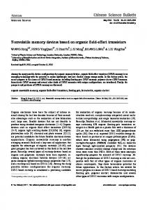
Fig. 1. (a) SEM image of Ni NCs spin-coated on a thermal oxide, (b) cross-sectional TEM image of Ni-NC floating gates sandwiched between the thermal oxide and the control oxide, and (c) a depth profile of the XPS spectra of Ni 2p orbits.
spin-coating condition was selected to ensure a densemonolayer NC array on the thermal oxide. A 15-nm-thick SiO2 film was deposited on the Ni NCs/5 nm SiO2 /Si substrate by using a low-pressure chemical vapor deposition method at 450 ◦ C. Subsequently, a 19-nm-thick Al2 O3 film was deposited at 300 ◦ C by using atomic layer deposition with trimethylaluminum and water. Finally, a 200 nm-thick Ni film was deposited on the Al2 O3 film to form a top electrode. A stacked structure of the control oxide (SiO2 /Al2 O3 ) was adopted to suppress charge tunneling from the gate metal to the Ni NCs, namely, back tunneling [11]. The top electrode (gate) was then patterned to a square of 100 × 100 µm2 by using photolithography processes and ion milling. Thus, a metal-oxide-semiconductor (MOS) cell with a Ni NC floating gate was fabricated for the Ni-NC nonvolatile memories (NVM). A planar image of the spin-coated Ni NCs on the thermal oxide was observed by using scanning electron microscopy (SEM). The cross-sectional structure of the MOS memory cell with Ni-NC floating gates was imaged by using transmission electron microscopy (TEM). A depth profile of X-ray photoemission spectroscopy (XPS) was measured to reveal the chemical bonding states of the Ni NCs embedded in the memory cell. Highfrequency C-V measurements were carried out by using an Agilent 4288A CV meter with a frequency of 1 MHz to investigate the charging/discharging characteristics of the Ni-NC MOS capacitors.
In Fig. 1(a), the SEM image shows Ni NCs distributed uniformly on a thermal oxide/Si substrate. The size and the areal density of Ni NCs are estimated as approximately 9 nm and 2 × 1011 cm−2 , respectively. Fig. 1 (b) shows a cross-sectional TEM image of Ni NCs embedded in a SiO2 matrix, in which almost one array of Ni NCs is located at a distance of about 4 nm from the SiO2 /Si interface. A combination of SiO2 and Al2 O3 was used as the control oxide. Depth-resolved X-ray photoemission (XPS) spectra can be obtained by taking the data with sputtering time. Fig. 1(c) shows XPS spectra of Ni 2p orbits as a function of depth from the surface of the MOS memory cell without a gate electrode. The results show that the Ni NCs remain as a metal throughout the NC area, except for the interface with a thermal oxide, where a Ni oxide seems to be formed. Fig. 2 shows C-V hysteresis loops of the memory capacitors for two sweep ranges, (+11, –11) and (+19, –19) V. The sweep range for characterizing flash memories is usually chosen within about ±20 V, which is comparable to that of conventional poly-silicon floating-gate memories. All samples show counterclockwise C-V hysteresis loops, indicating electron injection from the substrate to the charge trapping layer containing Ni NCs. The width in the hysteresis loop is about 18 V in the range of (+19, –19) V under a sweeping rate of 0.2 V/s. The MOS capacitors without Ni NCs showed just a few mV of memory window, meaning almost no memory effect. The program/erase (P/E) operations were performed using the Fowler-Nordheim (FN) tunneling method by applying ±19 V voltage pulses on the gate electrode of the devices. When the device is programmed, electrons tunnel from the Si substrate through the SiO2 barrier and are immediately relaxed to the Fermi level of the Ni NCs/trapped in their continuum states. On the contrary, electrons tunnel to the Si substrate through the barrier when the device is erased. Fig. 3 shows the
Nonvolatile Memory Devices Fabricated by Using Colloidal· · · – Kwang Soo Seol et al.
Fig. 3. P/E characteristics of the memory capacitor for a P/E voltage level (±19 V).
-51-
Fig. 5. Retention characteristics of the memory capacitor.
grammed/erased flat-band voltages show almost no significant degradation up to 104 cycles, indicating excellent endurance of the devices. The retention characteristics of the memory capacitor at room temperature are shown in Fig. 5. The programming was performed at +19 V for 10 ms and the erasing at –19 V for 0.1 s. Fast decay of the memory window is observed as time elapses. Extrapolation of the data up to 10 years shows that the initial memory window of 3.5 V drops to 0.8 V at room temperature. We suggest that the poor retention properties result from the lateral correlation of the Ni NCs due to their small separation of ∼2 nm relative to their size of ∼9 nm. Considering these results, further study is required to improve the retention properties for NVM applications. Fig. 4. Endurance characteristics of the memory capacitor.
IV. CONCLUSION P/E characteristics of the memory capacitors. The fullyprogrammed and fully-erased states are defined as those that were programmed by a pulse of (+19 V, 1 s) and erased by a pulse of (–19 V, 1s ), respectively. Memory windows of 3.3 ∼ 5.2 V are obtained at 10 ms – 1 s, respectively, which are relatively large compared to the previously-reported values for metal NC memories [5,6]. The amount of charge stored in the Ni NCs can be estimated by the relation Q = C ∆VM W , where C is the capacitance density and VM W is the memory window [12]. In this work, C and ∆VM W are about 1.4 × 10⁻⁷ F cm−2 and 3.3 ∼ 5.2 V, respectively, as shown in Fig. 2 and 3. Thus, the electron density stored in the NCs is estimated as (2.9 ∼ 4.6) × 1012 cm−2 , which is larger than the NC density obtained by using SEM and can be attributed to multiple electron storage in the Ni NCs or to the NC size distribution [12]. Fig. 4 shows the P/E cycling characteristics of the memory capacitor. Pulses of (+19 V, 10 ms) and (–19 V, 0.1 s) were applied to evaluate the endurance characteristics for the P/E operations, respectively. The pro-
Spin-coating of colloidal Ni NCs under controlled conditions without any heat treatment resulted in well formation of a single-layered Ni-NC array with a mean size of ∼9 nm and an areal density of 2 × 1011 cm−2 on thermal oxides. The isolation and the distribution of the Ni NCs were confirmed by using SEM and TEM. The MOS memory structures with the Ni-NC floating gates showed a relatively large memory window of 3 – 5 V for 10 ms – 1 s under ±19 V and excellent endurance characteristics.
REFERENCES [1] S. Tiwari, F. Rana, H. Hanafi, A. Harstein, E. F. Crabe and K. Chan, Appl. Phys. Lett. 68, 1377 (1996). [2] S. Kim, H.-S. Hwang, S.-H. Choi and K. J. Kim, J. Korean Phys. Soc. 48, 108 (2006). [3] S. Kim, S.-H. Choi, C. J. Park, H. Y. Cho and R. G. Elliman, J. Korean Phys. Soc. 49, 959 (2006).
-52-
Journal of the Korean Physical Society, Vol. 50, No. 1, January 2007
[4] B. De Salvo, C. Gerardi, S. Lombardo, T. Baron, L. Perniola, D. Mariolle, P. Mur, A. Toffoli, M. Gely, M. N. Semeria, S. Deleonibus, G. Ammendola, V. Ancarani, M. Melanotte, R. Bez, L. Baldi, D. Corso, I. Crupi, R. A. Puglisi, G. Nicotra, E. Rimini, F. Mazen, G. Ghibaudo, G. Pananakakis, C. M. Compagnoni, D. Ielmini, A. Lacaita, A. Spinelli, Y. M. Wan and K. van der Jeugd, Tech. Dig.-IEEE Int. Electron Devices Meet. (8-10 Dec. 2003), p. 26.1.1. [5] Z. Liu, C. Lee, V. Narayanan, G. Pei and E. C. Kan, IEEE Trans. Elec. Dev. 49, 1614 (2002). [6] J. Y. Tseng, C. W. Cheng, S.-Y. Wang, T.-B. Wu, K.-Y. Hsieh and R. Liu, Appl. Phys. Lett. 85, 2595 (2004). [7] S. Choi, S.-S. Kim, M. Chang, H. Hwang, S. Jeon and
C. Kim, Appl. Phys. Lett. 86, 123110 (2005). [8] M.-C. Daniel and D. Astruc, Chem. Rev. 104, 293 (2004). [9] V. F. Puntes, K. M. Krishnan and A. P. Alivisatos, Science 287, 1989 (2000). [10] J. Cho, K. Char, J.-D. Hong and K.-B. Lee, Adv. Mat. 13, 1076 (2001). [11] E. Spitale, D. Corso, I. Crupi, G. Nicotra, S. Limbardo, D. Deleruyelle, M. Gely, N. Buffet, B. DeSalvo and C. Gerardi, Proceeding of the 34th European Solid-State Device Research Conference (Essderc, 2004), p. 161. [12] Z. Tan, S. K. Samanta, W. J. Yoo and S. Lee, Appl. Phys. Lett. 86, 013107 (2005).