Novel Binary Linear Programming for High Performance Clock Mesh Synthesis Minsik Cho, David Z. Pan∗ and Ruchir Puri IBM T. J. Watson Research Center, Yorktown Heights, NY 10598 ∗ Dept. of ECE, The University of Texas at Austin, Austin, TX 78712
[email protected],
[email protected],
[email protected]
Abstract— Clock mesh is popular in high performance VLSI design because it is more robust against variations than clock tree at a cost of higher power consumption. In this paper, we propose novel techniques based on binary linear programming for clock mesh synthesis for the first time in the literature. The proposed approach can explore both regular and irregular mesh configurations, adapting to non-uniform load capacitance distribution. Our synthesis consists of two steps: mesh construction to minimize total capacitance and skew, and balanced sink assignment to improve slew/skew characteristics. We first show that mesh construction can be analytically formulated as binary polynomial programming (a class of nonlinear discrete optimization), then apply a compact linearization technique to transform into binary linear programming, significantly reducing computational overhead. Second, our balanced sink assignment enables a sink to tap the least loaded mesh segment (not the nearest one) with another binary linear programming which reduces both slew and skew. Experiments show that our techniques improve the worst skew and total capacitance by 14% and 15% over the state-of-the-art clock mesh algorithm [19] on ISPD09 benchmarks.
I. I NTRODUCTION With aggressive technology scaling to sub 32nm nodes, the impacts of process variation, power supply noise, and temperature fluctuation on clock network are becoming more critical [2], [14], [17], [24]. Such impacts result in larger clock skew, directly decreasing the performance of a VLSI system. Therefore, various design techniques to build more robust clock network have been introduced [6], [11]– [13], [15], [16], [18], [19], [22]. Among them, clock mesh with global clock tree in Fig. 1 has been shown to be highly effective in minimizing the impacts of PVT (process, voltage, and temperature) variations on clock skew [20], [21], thanks to the redundant current paths from a clock source to a sink. The key challenge in clock mesh design is to optimize two conflicting objectives, power dissipation and worst skew (e.g., variation tolerance) [2]. The redundant mesh structure makes clock skew less sensitive to the variations, but substantially increases total capacitance (leading to higher power consumption). In order to build more robust and power efficient clock mesh, various algorithms have been proposed. [4] proposed wire sizing for an existing clock mesh to reduce capacitance without degrading clock skew. [22] proposed set-covering based buffering and mesh reduction for a given mesh configuration to reduce power consumption while keeping similar variation tolerance. [19] suggested an iterative technique to determine a regular mesh configuration, followed by buffering and mesh reduction techniques both extended from [22]. However, most of existing approaches are either incrementally tuning a given clock mesh or lacking global planning. [7], [19] do not take non-uniform sink distribution and different clock domains into consideration upfront, resorting to post-processing step (e.g., mesh reduction), which may result in a sub-optimal clock mesh. In all previous work, a sink taps the nearest clock mesh segment, which is not necessarily the best decision when taking uneven sink capacitance distribution and buffering blockages into the account.
978-1-4244-8194-1/10/$26.00 ©2010 IEEE
Fig. 1. Illustration of a clock mesh driven by a buffered global clock tree, and clock sinks tapping the clock mesh through stub wires [19].
Lastly, the impact of clock mesh design on global clock tree has not been comprehensively analyzed/reported before. In this paper, we propose two novel binary linear programming formulations for clock mesh synthesis. The first one explores various (both regular and irregular) clock mesh configurations. It automatically determines the mesh dimension (rows and columns) and physical wire locations with lower skew at less power consumption, adapting to non-uniform load capacitance distribution (e.g., sink distribution or blockages). Once a clock mesh configuration is determined, the second binary linear programming is applied to assign each sink to the least loaded mesh segment in order to improve slew and skew. To our best knowledge, this is the first time that clock mesh synthesis is formulated in a rigorous mathematical programming manner, which 1) searches for the best trade-off between capacitance and skew and 2) targets for more uniform load capacitance distribution. The major contributions of this paper include the following: • We develop a simple/linear but high-fidelity skew bound model for clock mesh synthesis, which is incorporated into our clock mesh synthesis framework. • We propose a novel binary polynomial programming formulation for clock mesh synthesis, which is further linearized into binary linear programming based on [1] for lower computational overhead. Our formulation can explore both regular and irregular mesh configurations to determine the optimal mesh dimension (e.g., row/column) and find the best trade-off between skew and capacitance (or power). • We propose balanced sink assignment using binary linear programming in order to balance effective capacitance seen by each buffer, which will result in smaller slew and skew. We also take buffer blockages into consideration. The rest of the paper is organized as follows. Section II provides notations/assumptions in this work, and Section III presents our proposed algorithm. Experimental results are in Section IV, followed by the conclusion in Section V. II. N OTATIONS & A SSUMPTIONS s The notations in this paper are listed in Table I. lm is to measure distance between a sink s and a mesh candidate m during the mesh
438
TABLE I T HE NOTATIONS IN THIS PAPER . ro unit wire resistance co unit wire capacitance S a set of the sinks (indexed by s) ts latency to the sink s Cs load capacitance of the sink s V a set of vertical mesh candidates (indexed by v ) H a set of horizontal mesh candidates (indexed by h) Lm the length of the mesh candidate m s the minimum distance from the sink s to mesh candidate m lm W the stub (a wire from a sink to the clock mesh) length limit V s a set of mesh candidates ∈ V within W from the sink s H s a set of mesh candidates ∈ H within W from the sink s ls the stub length from the sink s to the (final) clock mesh lvs the vertical distance from the sink s to the clock mesh s lh the horizontal distance from the sink s to the clock mesh B the set of potential buffer locations (indexed by b) which are on the intersections of v ∈ V and h ∈ H bs the nearest buffer location b ∈ B from the sink s msb the Manhattan distance from the sink s to bs G a set of mesh segments from the final mesh (indexed by g ) Sg the length of a mesh segment g ng the number of unblocked buffer locations on a mesh segment g (0 ≤ ng ≤ 2)
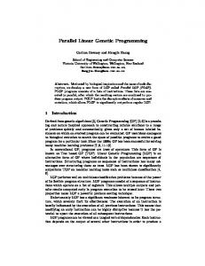
(a) Sink
distribution (b) Mesh candidates (c) Final clock mesh with mesh candidates selected by mesh after sink assignment in dashed lines. construction. and clean-up. Fig. 2.
Overall flow of the proposed algorithm.
constructed, we connect sinks to the clock mesh by solving the binary linear programming formulation in Section III-D while trying to uniformly distribute load capacitance. After removing any dangling wire segments, we will obtain the final clock mesh in Fig. 2 (c). B. Skew Bound Modeling
construction step in Section III-C, and ls denotes stub length between a sink and the final clock mesh which is built with a sub-set of V ∪H. If the stub from a sink s runs vertically to touch the final clock mesh, ls = lvs , otherwise ls = lhs . We assume that the clock buffers driving a clock mesh will be located at the cross-sections of mesh candidates [19], [22], as long as the location is unblocked [10] (e.g., the leaf level buffers in Fig. 1). These clock buffers become sinks to the global clock tree in Fig. 1. We additionally assume zero-skew and identical violation-free slew from a global clock tree to the inputs of these clock buffers. Also, while exploring various clock mesh configurations in our algorithm, we assume that a nominal strength buffer is placed at ∀b ∈ B. These assumptions on buffering are only to make our mesh synthesis less complex. Hence, more accurate buffer sizing (even removal) can be done after our flow. Even though we use a single wire type in this work (ro , co ), our techniques can be readily extended to handle various wire types.
Due to non-tree structure, an accurate analytical model for skew in clock mesh is currently unknown. Therefore, a skew bound is used in [19] to select the right mesh configuration. However, the skew bound in [19] is too complex to be used in an analytical optimization framework because it is nonlinear and requires full knowledge of mesh configuration. Hence, we propose a simpler/linear skew bound model to enable efficient analytical optimization of mesh configuration under the assumptions in Section II. Consider Fig. 3 where a sink i is right below a buffer b and sink j is connected to b through wire whose length is l. Cb is a parasitic/output capacitance in b and Ce represents any visible capacitance from b (e.g., other sinks and mesh segments in the proximity). Since i is right below b, we can regard that i is fully and solely driven by b. Then, the delay to i can be approximated as ti ≈ Rb (Cb + Ce + Ci + co l + Cj )
Meanwhile, j has some distance to b and may get partially driven by other buffers in the proximity. Therefore, by ignoring the currents from other buffers, we can compute the upper bound of tj as follows: co l + Cj ) (2) 2 Therefore, the worst latency difference in the proximity of b can be expressed as tj ≤ Rb (Cb + Ce + Ci + co l + Cj ) + ro l(
Kb
III. A LGORITHM In this section, we present our clock mesh synthesis. We begin with the overview in Section III-A. We propose a linear skew bound model for clock mesh in Section III-B, and then introduce our algorithm, which consists of mesh construction in Section III-C and balanced sink assignment in Section III-D. A. Overview Fig. 2 illustrates our algorithm flow. For a given input sink distribution, we create a set of horizontal/vertical clock mesh candidates as in Fig. 2 (a). Then, the binary linear formulation linearized from the binary polynomial formulation in Section III-C selects a set of mesh candidates to determine a mesh configuration as in Fig. 2 (b), minimizing total wire capacitance and skew bound based on Section III-B. Our formulation will not only automatically configure the dimensions of the clock mesh but also adjust the spacing between mesh wires from a given set of mesh candidates, accommodating non-uniform load capacitance distribution. Once a clock mesh is
(1)
= ≤ ≤
max({tj − ti |bi = bj = b}) co msb + Cs )|bs = b}) max({ro msb ( 2 max({ro msb (co W + Cs )|bs = b})
(3) (4) (5)
In detail, the latency difference between the sinks i and j is ro l( c2o l + Cj ) from Eq. (1) and (2). Thus, if we replace l with the longest msb (a Manhattan distance from a sink s to the buffer b = bs ), the skew in the proximity of b can be bounded by Eq. (4). However, as Eq. (4) is quadratic, it is expensive for optimization and cannot be used in a linear programming model. Since msb ≤ 2W (∀s ∈ S, ∀b ∈ B)
439
Rb
buffer
Cb Fig. 3.
rol Sink i
Ce
Ci
Sink j
col col 2
2
Cj
Simplified RC network to estimate the skew upper bound.
Estimated skew
1
s
l h1
0.8
W
0.6
W
S
s
S
l v1
W
s
l v3
l v4
h2
l h2 t
W
t
0.2
v1
0 0
0.1
0.2
0.3
0.4
0.5
0.6
Fig. 4.
due to Eq. (12) and (13), we can find a linearized skew bound in the proximity of b as in Eq. (5) (see Section III-C for details). msb is the key physical parameter which heavily affects the clock skew bound, and Eq. (5) implies that the longest distance from any sink to its nearest buffer has the first-order impact on the skew. msb can be computed as in Eq. (11), even when a clock mesh is being constructed. Then, we take the following as our skew bound: K = max({Kb |∀b ∈ B})
(6)
This is not the exact definition of skew (max({ts |s ∈ S}) − min({ts |s ∈ S})), as our scope is limited to the proximity of each buffer. However, our estimation is to obtain a skew bound rather than the real skew value, and we found that our skew bound model is practically sufficient enough for optimization. Fig. 4 shows the fidelity of our skew bound estimation based on 740 different clock mesh configurations. Our skew estimation always overestimates the skew from SPICE simulation and shows high-fidelity (r = 0.94). C. Mesh Construction In this section, we present our binary linear programming formulation for clock mesh construction. The inputs are a set of sinks and a set of vertical/horizontal mesh candidates as discussed in Fig. 2 (a), and the output is a set of mesh candidates selected under capacitance/skew consideration. Although we used a set of regularly spaced candidates in our implementation, a designer can add custom candidates if needed. For example, when a custom block or IP require a special clock pin access, some design-specific candidates can be prepared to meet the requirements. Let xm be a binary variable set to 1 if the mesh candidate m is selected (xm = 1 − xm ). Then, we can formulate mesh construction as follows:
P
s
l h3
h3
v3
v4
Skew bound estimation based on Eq. (6). Fig. 5.
co (
v2
(a) A set of mesh candidates for (b) 3 vertical and 3 horizontal mesh a sink s determined by W . candidates and their distances from s, when zoomed-in from (a).
Simulated skew from SPICE
s.t :
s
l v2 s
0.4
min :
h1
s
m∈V ∪V s
Lm +
P
s∈S
ls ) + αK
(7)
l = P (Vs ∪ Hs , s)
∀s ∈ S
lvs = P (Vs , s)
∀s ∈ S
(9)
lhs = P (Hs , s)
∀s ∈ S
(10)
ms = l s + l s
∀s ∈ S
(11)
v h Pb x ≥ 1 v P v∈Vs
(8)
∀s ∈ S
(12)
x ≥1 h∈Hs h
∀s ∈ S
(13)
K ≥ Kb
∀b ∈ B
(14)
xm ∈ {0, 1}
∀m ∈ V ∪ H
The objective in Eq. (7) is to minimize weighted summation of total wire capacitance and skew bound (α is a weight parameter). The total wire capacitance consists of two factors: one from the mesh candidates (Lm ) and the other from stubs (ls ) between the sinks and the clock mesh. lsv and lsh represent the vertical/horizontal distance to the final clock mesh. When connecting a sink s to a mesh, we only
Example of mesh candidates around the sink s within distance W .
consider the mesh candidates whose distance to s is shorter than W as in Fig. 5 (a), which form Vs and Hs depending on direction. In order to guarantee the final result forms a mesh, we need to pick at least one vertical and horizontal candidates around any sink within W as in Eq. (12) and (13) which explains msb ≤ 2W in Section III-B along with the buffer location assumption in Section II. Eq. (8) is to compute the shortest distance to any of selected mesh candidates in the proximity of a sink s. Eq. (11) is to compute msb , a Manhattan distance from a sink to the nearest buffer location, which will be used to compute skew bound based on Eq. (6) as in Eq. (14). The most challenging part of the formulation is how to compute lsv in Eq. (9), lsh in in Eq. (10), and ls in Eq. (8) which are the vertical/horizontal/shortest distances to the clock meshes, when the final clock mesh is unknown yet (we are in the process of selecting mesh candidates to construct the clock mesh). Since Eq. (9), (10), and (8) share the same goal (computing distance to the final mesh), we express these distances in a compact mathematical form covering all possible mesh candidate selections using a polynomial function P (U, s) without loss of generality, which is defined as follows: P (U, s) =
X
(lus
Y
xi xu )
(15)
{i|ls W ). Note that lhs and lvs can be computed by providing Vs and Hs respectively to Eq. (15). First, we can sort all the candidates in Vs ∪ Hs in the ascending order of distance from s, which leads to lhs 2 < lvs2 < lhs 1 < lvs3 < lhs 3 < lvs1 . Accordingly, we can assign higher priority to a mesh candidate with a shorter distance. The reason for prioritization is that once a mesh candidate with higher priority is selected, then other candidates with lower priorities can be ignored. Consider Table II which shows the value of ls depending on the selection of mesh candidates in Vs ∪Hs . For instance, if h2 is not selected but v2 is selected (the second row in Table II), then ls = lvs2 regardless of the remaining candidates, making them again as don’tcares, which is the exact behavior of priority encoder. By leveraging a binary representation of a priority encoder, we can express ls for the case in Fig. 5 (b) as following:
440
ls = P (Vs ∪ Hs , s)
=
lhs 2 xh2
+
lvs3 xh2 xv3
+
lhs 1 xh2 xv3 xh1
+
lvs3 xh2 xv3 xh1 xv3 lhs 3 xh2 xv3 xh1 xv3 xh3 lvs1 xh2 xv3 xh1 xv3 xh3 xv1
+ +
TABLE II T RUTH TABLE TO COMPUTE ls
Due to the nature of one-hot scheme, each term in Eq. (16) (also, Q
Y
xi
≡
z
z
≤
min({xi |i ∈ I})
z
≥
max(
(17)
i∈I
X
xi − |I| + 1, 0)
i∈I
Note that the auxiliary variable z can be declared as a continuous variable (helping the solver), since it will naturally be either 0 or 1 due to the linear constraints. Hence, based on Eq. (17), we can redefine a linearized P (U, s) with additional linear constraints for the optimization in Eq. (7) as below: P (U, s)
=
X
lu zu
(18)
u∈U
zu
≤
min({xi |lis < lus } ∪ {xu })
zu
≥
max(
X
xi + xu − |{i|lis < lus }|, 0)
{i|ls