e-Journal of Surface Science and Nanotechnology
30 June 2018
Conference - ISSS-8 -
e-J. Surf. Sci. Nanotech. Vol. 16 (2018) 313-319
Observation of Low-Energy Positron Diffraction Patterns with a Linac-Based Slow-Positron Beam∗ Ken Wada† Takasaki Advanced Radiation Research Institute, Quantum Beam Science Research Directorate, National Institutes for Quantum and Radiological Science and Technology, 1233 Watanuki, Takasaki, Gunma 370-1292, Japan
Tetsuroh Shirasawa National Metrology Institute of Japan, National Institute of Advanced Industrial Science and Technology, Tsukuba, Ibaraki 305-8565, Japan
Izumi Mochizuki Institute of Materials Structure Science, High Energy Accelerator Research Organization (KEK), 1-1 Oho, Tsukuba 305-0801, Japan
Masanori Fujinami Department of Applied Chemistry, Chiba University, 1-33 Yayoi, Inage, Chiba 263-8522, Japan
Masaki Maekawa and Atsuo Kawasuso Takasaki Advanced Radiation Research Institute, Quantum Beam Science Research Directorate, National Institutes for Quantum and Radiological Science and Technology, 1233 Watanuki, Takasaki, Gunma 370-1292, Japan
Toshio Takahashi Department of Physics, Tokyo Gakugei University, 4-1-1 Nukuikita, Koganei, Tokyo 184-8501, Japan
Toshio Hyodo Institute of Materials Structure Science, High Energy Accelerator Research Organization (KEK), 1-1 Oho, Tsukuba 305-0801, Japan (Received 9 February 2018; Accepted 5 May 2018; Published 30 June 2018) An experimental system has been developed for the study of low-energy positron diffraction (LEPD) with a slow-positron beam generated by a linear-electron-accelerator (linac). Diffraction patterns of a Ge(001)-2×1 surface structure have been observed with a normal positron incidence. This is the first LEPD observation with a linacbased high-intensity pulsed slow-positron beam. [DOI: 10.1380/ejssnt.2018.313] Keywords: Low energy positron diffraction (LEPD); Low energy electron diffraction (LEED); Positron spectroscopy; Germanium
I.
INTRODUCTION
Low-energy electron diffraction (LEED) is a powerful well-established tool for the structural determination of crystalline surfaces [1]. However, difficulties can arise on occasion in discerning the structure, especially of high atomic number (high-Z) materials, because of complex multiple scattering. Low-energy positron diffraction (LEPD), which is the positron counterpart of LEED, offers a solution to this problem and could become a more powerful tool for the study of surface structure. The first LEPD observation was carried out with a channel electron multiplier by the Brandeis group [2]. ∗
†
This paper was presented at the 8th International Symposium on Surface Science, Tsukuba International Congress Center, Tsukuba, Japan, October 22-26, 2017. Corresponding author:
[email protected]
The Brookhaven group first reported multiple-spot LEPD pattern with off-normal incidence [3]. Only the Brandeis group succeeded in observing multiple-spot LEPD pattern with normal incidence [4]. They developed an electrostatic slow-positron beam with a radioisotope (RI) source emitting positrons through β + -decay. The Brandeis group also demonstrated that in LEPD, experimental intensity profiles were more closely reproduced by the dynamical diffraction theory than in LEED [5–10]. Later theoretical works revealed that LEPD combines the advantages of (1) simple and smooth scattering factor, (2) less multiple scattering, and (3) higher surface sensitivity, so that the measured spectra can be accurately simulated for surface structural analysis. These advantages are summarized by Tong [11]. Firstly, the scattering factor of positrons more closely resembles that of X-rays than of electrons. An electron has sharp and complex angular anisotropies in magnitude and phase caused by bound and resonance states of the atomic potential. A positron and
c 2018 The Japan Society of Vacuum and Surface Science ISSN 1348-0391 ⃝
313
Wada et al.
Volume 16 (2018)
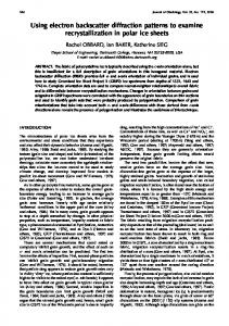
FIG. 1. Schematic view of the Slow Positron Facility at KEK (as of April 2018). Radiation shields are not shown. A slowpositron beam generated with a ∼50-MeV dedicated linac is guided by a magnetic field to the experimental hall and branched to stations, namely: the positronium negative ion (Ps– ) at the end of the SPF-B1; the positronium time-of-flight (Ps-TOF) at SPF-B2; and the total-reflection high-energy positron diffraction (TRHEPD) at SPF-A3. A new beam-line branch, SPF-A4, has been constructed for the LEPD experiment station.
a photon, however, have a smooth and simple scattering factor because of the absence of bound or resonance states. Secondly, while electrons are forward focused by a chain of atoms, thus producing strong multiple-scattering resonances in solids, positrons are not. The positron’s wavefield behind an atom is actually decreased, resulting in forward shadowing. This difference arises from the sign of the phase shifts; a repulsive (positron-atom) potential produces negative phase shifts while an attractive (electron-atom) potential produces positive phase shifts. Thirdly, the positron’s mean-free path is shorter than that of an electron’s below 200 eV because there are no excluded final states for the positron in the solid. Therefore, the positron is extremely sensitive to atomic positions in the first three or four layers of a solid surface. Despite these promising properties as an ideal technique for studying surface structure, no further experimental LEPD research has followed the pioneering work of the Brandeis group. The main reason for this is the difficulty in obtaining sufficient beam intensities to afford reasonable measurement times giving the required data quality for LEPD. It has long been hoped that the groundbreaking work of the Brandeis group over 20 years ago would be continued [12]. An attempt to develop a LEPD experiment system with a slow-positron beam generated by a normalconducting linear-electron-accelerator (linac) was once made at Lawrence Livermore National Laboratory [13]. They intended to take advantage of a high-intensity slowpositron beam generated by a linac, where positrons were obtained through positron-electron pair creation by bombarding high-energy electrons into a heavy metal. However, no report was published of an observation of a LEPD 314
pattern with this linac-based system. In the present study, we have developed a new LEPD system with a slow-positron beam generated by a linac at the High Energy Accelerator Research Organization (KEK), and succeeded in obtaining LEPD patterns of a Ge(001)-2×1 structure with normal incidence.
II.
LEPD SYSTEM AT THE SLOW POSITRON FACILITY, KEK A.
Linac-based slow-positron beam
The Slow Positron Facility (SPF) at the Institute of Materials Structure Science (IMSS) in KEK provides a high-intensity pulsed slow-positron beam generated using a dedicated normal-conducting linac operated at ∼50 MeV, < 0.6 kW with a repetition frequency of 50Hz [18, 19]. Accelerated electrons are impacted on a tantalum (Ta) plate and deflected in the electric field around the Ta atom, emitting Bremsstrahlung X-rays. Radiation with energy greater than 2mc2 = 2 × 511 keV causes positron-electron pair creation in the same metal. The energy range of the generated positrons is large, up to almost 50 MeV. The Ta plate used for this process is called the electron-positron converter, or simply the converter. A moderator, which is composed of tungsten (W) films with thickness 25 µm, is then used to obtain monoenergetic positrons (slow positrons). When high-energy positrons penetrate a metal, they are thermalized in the bulk and most annihilate with electrons. However, in metals with a negative positron work function such as W, Ni, J-Stage: https://www.jstage.jst.go.jp/browse/ejssnt/
e-Journal of Surface Science and Nanotechnology
Gate valve
Volume 16 (2018)
Chamber for atomic hydrogen cleaning 125 mm
Magnetic coils
Magnetic lens
Gate valve
+ Sample holder Remoderator Electrostatic lenses
DLD MCP
Gap EL1
Deflectors
EL2
Sample holder Mu-metal Ni Remoderator W Plate Mu-metal
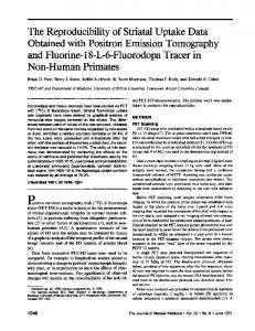
FIG. 2. (a) The present LEPD experimental station. (b) Detailed figure of the area surrounded by the dashed line in (a) showing the electrostatic potential with a color gradient, and simulated beam trajectories.
and Cu, a proportion of the positrons are emitted after thermalization with an energy corresponding to the work function. This slow-positron generating process occurs within picosecond time order, so the time structure of the slow-positron beam reflects that of the pulsed electron beam accelerated by the linac. The slow-positron production unit, composed of the converter and the moderator, is kept at 0.1–35 kV with respect to the grounded slow-positron beam line, so that the moderated positrons are accelerated immediately after exiting the unit. The accelerated positrons, with an energy of 0.1–35 keV are transported by a magnetic field generated using a series of coils aligned along the beam-line duct to the experimental hall and branched to different stations, as shown in Fig. 1. There are three experimental stations, namely: the positronium negative ion (Ps– ) at the end of the SPF-B1; the positronium time-of-flight (Ps-TOF) at SPF-B2; and the total-reflection high-energy J-Stage: https://www.jstage.jst.go.jp/browse/ejssnt/
positron diffraction (TRHEPD) at SPF-A3. For the LEPD experiment, a new beam-line branch was constructed, SPF-A4, which was extended from the branching point of SPF-A3. The vacuum pressure of the beam-line duct is maintained at ∼1 × 10⁻⁷ Pa with ion pumps after baking. The diameter of the magnetically transported beam is ∼10 mm. The beam intensity is approximately + 7 10 slow-e /s with an energy of 5 keV.
B.
Pulse stretcher for a linac-based slow-positron beam with an energy of 5 keV
There are a number of differences between an RI-based LEPD system and a linac-based one. One difference is the time structure of the beam. While an RI-based system provides a continuous beam owing to the Poisson random process for positron emission through β + -decay, a slow315
Wada et al.
Volume 16 (2018)
TABLE I. A list of voltages applied to the remoderator (RM), the first hemispherical grid nearest to the sample (Grid #1), the second grid (Grid #2), the third grid (Grid #3), the front side of the MCP (MCP front), and the back side of the MCP (MCP back) in volts. The remoderator bias is 50 V < VRM < 300 V.
RM VRM
Grid #1 GND
Grid #2 VRM − 10
positron beam generated with a normal-conducting linac has a pulsed time-structure reflecting that of the linac beam. For example at the SPF in KEK, the maximum beam intensity is obtained with a pulse width of 1.2 µs at a rate of 50 Hz. There are ∼106 slow-e+ in every pulse, which is a positron density per unit time within a pulse of ∼1012 slow-e+ /s. For the LEPD experiment, a twolayer delay-line detector (DLD) with micro-channel plates (MCP) was introduced [16, 17]. This is a counting-based detection system, which obtains the position of the particles incident on the MCP, and has a limited allowance of ∼100 ns for the time between two hits. In this time range, ∼105 slow-e+ exist in the primary beam, and those could cause a multi-hit problem in this set-up. To address this issue, a pulse stretcher was incorporated. The pulse stretcher, developed for a linac-based slowpositron beam with an energy of up to 5 keV is a linear storage system for the positrons, made up of cylindrical electrodes and magnetic solenoid coils. Details will be described elsewhere [20]. The stretcher consists of a grounded electrode, an entrance electrode, a 6-m long trapping electrode, an exit electrode, and another grounded electrode, all contained within the beam-line duct. The solenoid coils for the beam transportation are used to confine the positrons longitudinally along the beam-line. Positrons with an energy of 5.0 ± 0.05 keV are trapped between the entrance electrode at 5.75 kV and the exit electrode at 5.2 kV. To allow the 1.2-µs wide positron pulse into the trap, the entrance electrode voltage is temporarily lowered to 4.5 kV. Positrons are slowed down in the gap between the grounded electrode and the entrance electrode, pass through the entrance electrode, and are slowed down further in the gap between the entrance and the trapping electrode held at 4.74 kV. The positrons travel along the magnetic field down to the exit electrode where they are reflected back. Before they reach the entry point, the entrance electrode potential is raised back to 5.75 kV thus trapping the positrons. By gradually increasing the trapping electrode voltage, positrons spill over the exit electrode. The pulse width of the spilled positrons is controlled by adjusting the sweeping speed of the trapping electrode voltage. For the present LEPD system, the pulse width was stretched to ∼200 µs, which is the minimum width limited by the frequency response of the high-voltage amplifier used for controlling the ramping-electrode voltage. This pulse width is sufficiently large to avoiding the multiplehit problem at the DLD and will give the minimum background signals caused by the dark current in the MCP by filtering the data with the positron detection timing as is described in Sec. II D. 316
Grid #3 VRM − 10
C.
MCP front VRM − 330
MCP back VRM + 2070
Brightness enhancement system and LEPD optics
Another difference between the RI-based system and the linac-based system for LEPD experiments is the beam transportation methods. The RI-based LEPD system employed electrostatic lenses along the whole beam-line, while linac-based systems transport the beam along a magnetic field aligned with the beam-line. Since X/γrays and neutrons generated in a linac operation must be shielded from and sufficiently reduced at the point of experiment, a slow-positron beam is usually transported some distance from its production unit, typically more than 10 m. Such distances are difficult with electrostatic transportation, therefore linac-based slow-positron beams have been magnetically transported. However, for diffraction experiments, positrons must interact with the sample in a non-magnetic space and have sufficient beam quality in order to acquire meaningful data. So far, two kinds of positron diffraction experiments with a linac-based system have been realized: transmission positron diffraction with a transmission positron microscope (TPM) [14] and total-reflection high-energy positron diffraction (TRHEPD) [15]. Compared to the high-energy beams used in the other systems (30 keV for TPM and 10 keV for TRHEPD), typical LEPD beam energies are low, from ∼50 eV to ∼300 eV. Since the beam trajectory of such low-energy positrons can be significantly affected by the magnetic field from the beam-line, special care must be taken. To obtain positrons in the non-magnetic space with sufficient beam quality for LEPD, we have constructed a set-up using a transmission-type remoderator [21–25] of Ni(100) foil with thickness 150 nm, a magnetic lens, and electrostatic lenses shielded by Mu-metal, as shown in Fig. 2. Coils before the magnetic lens produce a typical magnetic field along the beam line of ∼10 mT. The last coil prior to the magnetic lens generates a field in the reverse direction, so that the field strength decreases rapidly downstream. The 5.2-keV positron beam is introduced into the magnetic lens, which focuses it onto the Ni remoderator, where the beam diameter is ∼3 mm. A Ni ring of diameter 2 mm is placed on the incident side of the remoderator to eliminate the outer positrons, which may result in a beam with a large diameter and divergence. Figure 2(b) shows the non-magnetic region in detail. Here, the positrons are focused onto the remoderator, thermalized, and a proportion are re-emitted with an energy of 1 eV, which corresponds to the negative positron work function of Ni. Approximately 90% of the beam intensity is lost in this process, however the brightness J-Stage: https://www.jstage.jst.go.jp/browse/ejssnt/
e-Journal of Surface Science and Nanotechnology
Volume 16 (2018)
is enhanced by ∼1000 times. The brightness, B, of the slow-positron beam is defined as [26] B=
I r2 θ2 E
,
where I is the beam intensity, r is the beam radius, θ is the angular spread of the beam, and E is the beam energy. Liouville’s theorem shows that the denominator of the brightness expression keeps a constant value in a nondissipative force field. After remoderation, the value of the denominator becomes of the order of 1/10000 of that before the remoderation, with almost the same r, smaller θ, and significantly reduced E by a dissipative force during the thermalization. In the present system, the positron injection energy onto the remoderator is 5.2 keV, and the re-emitted positron energy is 1 eV, producing a higher quality beam albeit at the expense of intensity. The reemitted positrons are extracted from the back of the Ni remoderator and electrostatic lenses transport them to the grounded sample. The final kinetic energy of the beam impinging on the sample is determined by the potential at the remoderator, VRM , and the negative work function to be (VRM + 1) eV. The re-emitted positrons are accelerated by the electric field between the cathode, on which the remoderator is mounted, and a grounded extraction electrode. Then two sets of einzel lenses transport the beam to the sample. The electrostatic potentials for the first einzel lens (EL1) and the second (EL2) are set to be ∼55% and ∼60% with respect to that at the remoderator, respectively. Figure 2(b) shows the electrostatic potential with a color gradient, and also simulated beam trajectories. Two sets of 8-pole deflectors [27] are placed between the two einzel lenses to adjust the beam trajectory. This electrostatic lens system keeps the full width of the beam diameter at half maximum intensity (FWHM) at ∼1.5 mm and the angular divergence < 2◦ at an energy of 50–300 eV on the sample. The entire LEPD optics for the remoderated beam is surrounded by a Mu-metal cylinder of thickness 1 mm to give shielding from the magnetic field produced by the magnetic lens and coils. Mu-metal was also used for the remoderator mount to cap the Mu-metal cylinder. A small gap between the Mu-metal cathode and Mu-metal cylinder keeps the electrostatic potential of the cathode from the grounded cylinder. Prior to introduction into the LEPD system, the Ni remoderator was annealed in a hydrogen furnace. Then, in a small chamber above the beam line, the surface of the Ni remoderator was cleaned by exposure to atomic hydrogen just before use. The whole LEPD chamber is surrounded by correction coils to cancel the effect of the Earth’s magnetic field on the beam trajectory.
D.
Detection system
The detection system is composed of three hemispherical grids, a chevron MCP stack, and a DLD, all with a J-Stage: https://www.jstage.jst.go.jp/browse/ejssnt/
FIG. 3. A 2D histogram of pulse heights of the MCP signals and the detection time relative to the linac trigger. A 1D histogram of the pulse height distribution (left) and that of detected time relative to the linac trigger (bottom) are also shown. The data used for analysis is shown by the solid rectangular in the 2D histogram.
central hole. The development of a LEED system with a DLD from RoentDek Handels GmbH is reported elsewhere in detail [28]. In the present study, a DLD-LEED system from OCI Vacuum Microengineering Inc. is used after removing the electron gun and placing in the LEPD optics as described above. The voltages applied to the remoderator (RM), the first hemispherical grid nearest to the sample (Grid #1), the second grid (Grid #2), the third grid (Grid #3), the front of the MCP (MCP front), and the back of the MCP (MCP back) are listed in Table I. The remoderator bias, VRM , is set to a value of 50– 300 V. The sample and Grid #1 are grounded, while Grid #2 and Grid #3 are held at 10 V below the remoderator bias to prevent inelastically scattered positrons from reaching the MCP. The incident energy of the diffracted positrons to the front of the MCP is (330 + 1) eV for all VRM , so that the efficiency of the avalanche process in the MCP is almost saturated for all the LEPD energies. The negative bias voltages at the front of the MCP prevent the detection of most of the secondary electrons from being detected. To improve the signal-to-noise ratio, the background signal caused by γ-rays from positron-electron pair annihilation must be reduced. A 10-mm thick W base plate is placed in front of the DLD, as shown in Fig. 2(b), to shield the detector from the annihilation γ-rays emitted at the remoderator and the electrostatic lenses. The detection efficiency of the MCP for 511-keV γ-ray is of the order of 0.1%. In addition, the background caused by annihilation γ-rays and the dark current is reduced by filtering the data with the pulse height of the MCP signal and the detection time relative to the linac trigger. A 2D histogram of pulse heights of the MCP signals and the detection time relative to the linac trigger is plotted in Fig. 3. A 1D histogram of the pulse height distribution 317
Wada et al.
Volume 16 (2018)
FIG. 4. Diffraction pattern of a Ge(001)-2×1 structure observed with a 144.5-eV positron beam. The data was accumulated over a four hour period.
(PHD) and that of detected time relative to the linac trigger are also shown. The PHD for the γ-rays and that for the dark current has an exponentially decaying shape, but the PHD for charged particles is Gaussian [29]. The minimum threshold for the MCP pulse height is set at the 515th channel, which is shown by a horizontal dashed line in Fig. 3. Since the pulse width of the slow-positron beam is adjusted to ∼200 µs with a 20-ms repetition, the relevant data is also filtered by setting the time window as shown by the vertical dashed lines in Fig. 3. The data filtered with these limits is shown by the solid rectangular in the 2D histogram.
III.
EXPERIMENT
The samples observed were cut from a mirror-polished flat Ge(001) wafer (non-doped, R ∼ 2 kΩ at room temperature). A clean Ge(001)-2×1 surface was prepared by sputtering with 800-eV Ar+ ions at 670 K for 10 min and annealing at the same temperature for 15 min. For the LEPD observations, the sample temperature was lowered to 120 K using a refrigerator in order to obtain brighter spots by reducing ineleastic positron–phonon scattering, i.e. the Debye-Waller effect. The base pressure of the LEPD chamber was 2 × 10⁻⁸ Pa at room temperature. LEPD observation run-times were several hours in length. To check the signal/background count rate, a further background observation run was conducted with the Grid #2 and #3 voltages at (VRM + 2) V, so that all positrons were repelled.
IV.
RESULTS AND DISCUSSION
Figure 4 displays an example of a diffraction pattern accumulated over a five hour period with a 144.5-eV
318
positron beam. Integer and fractional order spots from the 2 × 1 structure are clearly recognized. There is a “+” shaped dead zone in the diffraction pattern obtained. The design of an DLD anode with a central hole requires a gap in the wiring of the delay-line layers [28]. A LEPD I-V curve analysis, for example, is possible with this dead zone because the intensity of chosen spots are observed for the analysis. Due to the detector being flat (consisting of the flat MCP and the DLD), the appearance of the spots shown in Fig. 4 is elongated along the radius direction compared to those from a conventional LEED system with a hemispherical screen. Some spots located near the edges of the “+” shaped dead zone are distorted because of a nonlinearity near the edge of the gap on the DLD [28]. With the cut-off conditions of the PHD and the timing from the linac trigger, the number of γ-rays detected is reduced by ∼60%, while that of positrons is reduced by ∼15%. The ratio of the count rate for the γ-rays to that for the positrons in the whole area of the detector with and without the cut-off conditions is ∼10 and ∼5, respectively. In addition to the ordinary I-V curve analysis, possible applications with the present LEPD system is surface holography [30] and the analysis with the surface Patterson function by inversion of LEPD I-V Spectra [31]. For surface holography, adatoms and dimers on the surface of the sample substrate are used as a beam splitter for object and reference waves for holographic reconstruction. A calculation shows that LEPD is better suited than LEED for the holographic artifact-free reconstruction [30].
V.
CONCLUSION
An experimental system has been developed to obtain low-energy positron diffraction patterns using a normal conducting linac-based high-intensity slow-positron beam. Pulsed magnetically guided positrons, have been remoderated in an electrostatic system to produce a highintensity brightness-enhanced beam. Diffraction patterns were obtained, showing clearly Ge(001)-2×1 structure with integer and fractional order spots. This is the first observation of diffraction patterns using this method, demonstrating the feasibility of developing this technique as a tool for surface analysis.
ACKNOWLEDGMENTS
This work was supported by MEXT/JSPS KAKENHI Grant Numbers JP24221007 and JP16K13692, Toray Science and Technology Grant, the Cross Ministerial Strategic Innovation Promotion Program (SIP, unit D66). Experiments were conducted under the approval of the PF PAC (Proposal Nos. 2014G636, 2015S2-002, 2016S2-001, 2016S2-006) and under the auspices of the QST- KEK Joint Development Research.
J-Stage: https://www.jstage.jst.go.jp/browse/ejssnt/
e-Journal of Surface Science and Nanotechnology
[1] M. A. Van Hove, H. W. William, and C. M. Chan, LowEnergy Electron Diffraction: Experiment, Theory and Surface Structure Determination (Springer, Berlin, Heidelberg, 1986). [2] I. J. Rosenberg, A. H. Weiss, and K. F. Canter, Phys. Rev. Lett. 44, 1139 (1980). [3] W. E. Frieze, D. W. Gidley, and K. G. Lynn, Phys. Rev. B 31, 5628 (1985). [4] T. N. Horsky, Semiconductor Surface Structure Determination via Low Energy Positron Diffraction: Cleavage Faces of Cadmium-Selenide, Ph. D. thesis, Brandeis University, 1989. [5] T. N. Horsky, G. R. Brandes, K. F. Canter, C. B. Duke, S. F. Horng, A. Kahn, D. L. Lessor, A. P. Mills, Jr., A. Paton, K. Stevens, and K. Stiles, Phys. Rev. Lett. 62, 1876 (1989). [6] C. B. Duke, D. E. Lessor, T. N. Horsky, G. Brandes, K. F. Canter, P. H. Lippel, A. P. Mills Jr., A. Paton, and Y. R. Wang, J. Vac. Sci. Technol. A 7, 2030 (1989). [7] T. N. Horsky, G. R. Brandes, K. F. Canter, C. B. Duke, A. Paton, D. L. Lessor, A. Kahn, S. F. Horng, K. Stevens, K. Stiles, and A. P. Mills Jr., Phys. Rev. B 46, 7011 (1992). [8] D. L. Lessor, C. B. Duke, X. M. Chen, G. R. Brandes, K. F. Canter, and W. K. Ford, J. Vac. Sci. Technol. A 10, 2585 (1992). [9] X. M. Chen, K. F. Canter, C. B. Duke, A. Paton, D. L. Lessor, and W. K. Ford, Phys. Rev. B 48, 2400 (1993). [10] C. B. Duke, A. Paton, A. Lazarides, D. Vasumathi, and K. F. Canter, Phys. Rev. B 55, 7181 (1997). [11] S. Y. Tong, Surf. Sci. 457, L432 (2000). [12] P. G. Coleman, Appl. Surf. Sci. 194, 264 (2002). [13] A. Hamza, P. Asoka-Kumar, W. Stoeffl, R. Howell, D. Miller, and A. Denison, Radiat. Phys. Chem. 68, 635 (2003). [14] M. Matsuya, S. Jinno, T. Ootsuka, M. Inoue, M. Doyama, M. Inoue, and M. Fujinami, Nucl. Instrum. Methods Phys. Res. A 645, 102 (2011).
J-Stage: https://www.jstage.jst.go.jp/browse/ejssnt/
Volume 16 (2018)
[15] M. Maekawa, K. Wada, Y. Fukaya, A. Kawasuso, I. Mochizuki, T. Shidara, and T. Hyodo, Eur. Phys. J. D 68, 165 (2014). [16] S. E. Sobottka and M. B. Williams, IEEE Trans. Nucl. Sci. 35, 348 (1988). [17] O. Jagutzki, V. Mergel, K. Ullman-Pfleger, L. Spielberger, U. Spillmann, R. Dorner, and H. Schmidt-B¨ ocker, Nucl. Instrum. Methods Phys. Res. A 477, 244 (2002). [18] K. Wada, T. Hyodo, A. Yagishita, M. Ikeda, S. Ohsawa, T. Shidara, K. Michishio, T. Tachibana, Y. Nagashima, Y. Fukaya, M. Maekawa, and A. Kawasuso, Eur. Phys. J. D 66, 37 (2012). [19] K. Wada, T. Hyodo, T. Kosuge, Y. Saito, M. Ikeda, S. Ohsawa, T. Shidara, K. Michishio, T. Tachibana, H. Terabe, Y. Nagashima, Y. Fukaya, M. Maekawa, I. Mochizuki, and A. Kawasuso, J. Phys.: Conf. Ser. 443, 012082 (2013). [20] K. Wada, M. Masaki, I. Mochizuki, A. Kawasuso, M. Kimura, and T. Hyodo, in preparation. [21] A. P. Mills Jr. and R. J. Wilson, Phys. Rev. A 26, 490 (1982). [22] D. M. Chen, K. G. Lynn, R. Pareja, and B. Nielsen, Phys. Rev. B 31, 4123 (1985). [23] N. Zafar, J. Chevallier, G. Laricchia, and M. Charlton, J. Phys. D: Appl. Phys. 22, 868 (1989). [24] N. Oshima, R. Suzuki, T. Ohdaira, A. Kinomura, T. Narumi, A. Uedono, and M. Fujinami, J. Appl. Phys. 103, 094916 (2008). [25] M. Fujinami, S. Jinno, M. Fukuzumi, T. Kawaguchi, K. Oguma, and T. Akahane, Anal. Sci. 24, 73 (2008). [26] A. P. Mills, Jr., Appl. Phys. 23, 189 (1980). [27] R. G. E. Hutter, in: Advances in Image Pickup and Display, edited by B. Kazan (Academic Press, New York, 1974) p. 163. [28] D. Human, H. F. Hu, C. J. Hirschmugl, J. Ociepa, G. Hall, O. Jagutzki, and K. Ullmann-Pfleger, Rev. Sci. Instrum. 77, 023302 (2006). [29] J. L. Wiza, Nucl. Instrum. Methods 162, 587 (1979). [30] S. Y. Tong, H. Huang, and X. Q. Guo, Phys. Rev. Lett. 69, 3654 (1992). [31] H. Wu and S. Y. Tong, Phys. Rev. Lett. 87, 036101 (2001).
319