minimum clock period and for selecting a range of process- tolerant clock skews ... storage elements, called the permissible range [7] or certainty region [8], as ...
Optimal Clock Skew Scheduling Tolerant to Process Variations José Luis Neves and Eby G. Friedman University of Rochester Department of Electrical Engineering Rochester, New York 14627 Abstract1- A methodology is presented in this paper for determining an optimal set of clock path delays for designing high performance VLSI/ULSI-based clock distribution networks. This methodology emphasizes the use of non-zero clock skew to reduce the system-wide minimum clock period. Although choosing (or scheduling) clock skew values has been previously recognized as an optimization technique for reducing the minimum clock period, difficulty in controlling the delays of the clock paths due to process parameter variations has limited its effectiveness. In this paper the minimum clock period is reduced using intentional clock skew by calculating a permissible clock skew range for each local data path while incorporating process dependent delay values of the clock signal paths. Graph-based algorithms are presented for determining the minimum clock period and for selecting a range of processtolerant clock skews for each local data path in the circuit, respectively. These algorithms have been demonstrated on the ISCAS-89 suite of circuits. Furthermore, examples of clock distribution networks with intentional clock skew are shown to tolerate worst case clock skew variations of up to 30% without causing circuit failure while increasing the system-wide maximum clock frequency by up to 20% over zero skew-based systems.
storage elements, called the permissible range [7] or certainty region [8], as shown in Figure 1. A violation of the lower bound leads to circuit failure while a violation of the upper bound limits the clock frequency of the circuit. Based on these observations, the process variation tolerant optimal clock skew scheduling problem can be divided into two sub-problems: determining a minimum clock period that defines a valid permissible range for any two storage elements in the circuit, and determining a minimum width for each permissible range such that unacceptable variations in the target clock skew remain within the bounds of a permissible range. In this paper, a solution for this problem is presented.
1. INTRODUCTION
The problem of determining a minimum clock period has been previously solved [1, 3-6] in which a set of timing equations is used to determine the optimal clock period and the clock delay to each register in the circuit, thereby defining the local clock skews. However, in order to better control the effects of process parameter variations, it is advantageous to determine the permissible range of each local data path, select a clock skew value that allows a maximum variation of skew within the permissible range and, finally, determine the clock delays to each register. This paper is organized as follows: in Section 2, a localized clock skew schedule is derived from the effective permissible range of the clock skew for each local data path considering any global clock skew constraints and process parameter variations. In Section 3, techniques for determining the set of clock skew values that are tolerant to process parameter variations are presented. In Section 4, these results are evaluated on a series of benchmark circuits, thereby demonstrating performance improvements and immunity to process parameter variations. Finally, some conclusions are drawn in Section 5.
Clock skew occurs when the clock signals arrive at sequentially-adjacent storage elements at different times. Although it has been shown that intentional clock skew can be used to improve the clock frequency of a synchronous circuit [1, 2, 3, 4, 5, 6], clock skew is typically minimized when designing the clock distribution network, since unintentional clock skew due to process parameter variations may limit the maximum frequency of operation, as well as cause circuit failure independent of the clock frequency (i.e., race conditions). In [1,2], it is demonstrated that double clocking (the effect of the same clock pulse triggering the same data into two adjacent storage elements) can be prevented when the clock skew between these storage elements satisfies TSkewij ≥ - TPDmin, where TPDmin is the minimum propagation delay of the path connecting both storage elements. Furthermore, it is also shown in [1,2] that zero clocking (the data reaches a storage element too late relative to the following clock pulse) is prevented when TSkewij ≤ TCP - TPDmax, where TCP is the clock period and TPDmax is the maximum propagation delay of the data path connecting both storage elements. The limits of both inequalities, TSkewij(min) = -TPDmin and TSkewij(max) = TCP - TPDmax, define a region of valid clock skew for each pair of adjacent
1This research was supported by Grant 200484/89.3 from CNPq (Conselho Nacional de Desenvolvimento Científico e Tecnológico) Brazil, the National Science Foundation under Grant No. MIP-9208165 and Grant No. MIP-9423886, the Army Research Office under Grant No. DAAH04-93-G-0323, and by a grant from the Xerox Corporation
Local data path In
Ci Race Conditions
TPD(min)
Ri
TSkewij = TCDi - TCDj
Out
Cj
Permissible range
A −∞
Rj
/TPD(max)
Clock Period Limitations
B TSkewij(min)
C TSkewij(max)
∞
Clock skew range (time)
Figure 1: Permissible range of a local data path.
2. OPTIMAL CLOCK SKEW SCHEDULING A synchronous digital circuit C can be modeled as a finite directed multi-graph G(V,E). Each vertex in the graph, vj ∈ V, is associated with a register, circuit input, or circuit output. Each edge in the graph, eij ∈ E, represents a physical connection between vertices vi and vj, with an optional combinational logic path between the two vertices. An edge is a bi-weighted connection representing the maximum (minimum) propagation delay TPDmax (TPDmin) between two sequentially-adjacent storage elements, where TPD includes the register, logic, and interconnect delays of a local data path [7]. A local data path Lij is a set of two vertices connected by an edge, Lij = {vi, eij, vj} for any vi, vj ∈V. A global data path Pkl = v k p → v l is a set of alternating edges and vertices {vk, ek1, v1, e12, ..., en-1l, vl}, representing a physical
33rd Design Automation Conference Permission to make digital/hard copy of all or part of this work for personal or class-room use is granted without fee provided that copies are not made or distributed for profit or commercial advantage, the copyright notice, the title of the publication and its date appear, and notice is given that copying is by permission of ACM, Inc. To copy otherwise, or to republish, to post on servers or to redistribute to lists, requires prior specific permission and/or a fee. DAC 96 - 06/96 Las Vegas, NV, USA 1996 ACM, Inc. 0-89791-833-9/96/0006.. $3.50
connection between vertices vk and vl, respectively. A multi-input circuit can be modeled as a single input graph, where each input is connected to vertex v0 by a zero-weighted edge. Also, Pl(Lij) is defined as the permissible range of a local data path and Pg(Pkl) the permissible range of a global data path. Finally, the clock skew of a local data path is defined as TSkewij(Lij) = TCDi - TCDj, where TCDi and TCDj are the clock signal delays of vertices vi and vj. The clock skew is described as negative if TCDi precedes TCDj (TCDi < TCDj) and as positive if TCDi follows TCDj (TCDi > TCDj). 2.1 Timing Constraints The timing behavior of a circuit C can be described in terms of two sets of timing constraints, local constraints and global constraints. The local constraints ensure the correct latching of data into the registers of a local data path, i.e., to prevent double and zero clocking. The local timing constraints are represented by the following equation [1-6] to prevent zero clocking, TSkew ( Lij ) ≥ THoldj − TPD (min) + ζ ij
,
(1)
and the following equation to prevent double clocking, TSkew ( Lij ) ≤ TCP − TPD (max)
,
(2)
where ζij is a safety term introduced in [7] to prevent race conditions due to process parameter variations, as described in Section 3. Satisfying the permissible range of each local data path Pl(Lij), however, does not guarantee a race-free circuit, particularly when there are multiple parallel and feedback data paths between two vertices. Two paths with common vertices are said to be in parallel when the signal data flows in the same direction in both paths. Likewise, a path is a feedback path when the data signal flows in a direction that is the reverse direction of the data signal flowing from the input of the circuit to the output of the circuit. To illustrate this situation, consider a circuit composed of several global data paths connecting two common vertices vo and vl, as shown in Figure 2. The vertices vo and vl represent two registers, each register driven by a single clock signal, where the clock skew between vo and vl is unique and independent of the path connecting vo to vl. A valid clock skew between vo and vl only exists if the clock skew is common to all the global data paths connecting vo and vl. Since the clock skew between vertices vo and vl is also the sum of the clock skew of each cascaded local data path connecting vo to vl [9], the resulting sum is independent of the global path between vo to vl. Alternatively, the permissible range of each of the paths connecting the vertices vo and vl is the sum of the permissible range of each cascaded local data path (lighter-shaded regions in Figure 2) between vo and vl, independent of the path between vo and vl. Therefore, a clock skew between the vertices vo and vl exists if the intersection of the permissible ranges of the paths connecting vo and vl form a nonempty set (darker-shaded regions in Figure 2) [9]. Pl(
Pl(Lij)
) L 0i
vi Pl(L0k)
v0
Pg(P0j) =Pl(L0i) + Pl(Lij)
vj
Pl(Lkl)
vk
Pg(P0l) = Pg(P0l) ∩ Pg(Pl0)
vl
Pl(Ll0)
Figure 2: Example of matching permissible ranges in a circuit with parallel and feedback paths From the example in Figure 2, in order to prevent circuit failures at the global level, circuits with parallel and feedback
paths must have a non-empty permissible range composed of the intersection or overlap among the permissible ranges of each individual parallel and feedback path. Therefore, a new set of global timing constraints are required and formalized below. The concept of permissible range overlap of a global data path Pkl can be stated as follows: Theorem 1: Let Pkl ∈ V be a global data path within a circuit C with m parallel and n feedback paths. Let the two vertices, vk and vl ∈ Pkl, which are not necessarily sequentially-adjacent, be the origin and destination of the m parallel and n feedback paths, respectively. Also, let Pg(Pkl) be the permissible range of the global data path composed of vertices vk and vl. Pg(Pkl) is a nonempty set of values iff the intersection of the permissible ranges of each individual parallel and feedback path is a non-empty set, or
( )
m Pg ( Pkl ) = � Pg Pkli i=1
� � Pg(Plkj ) ≠ ∅
n j =1
.
(3)
Proof ⇒: The clock skew between vertices vk and vl, TSkewkl, is unique and independent of the number of paths connecting the two vertices. Also, the clock skew TSkewkl of a single path that connects both vertices is the sum of the clock skew of each local data path along the path. Assuming that a value of clock skew exists between vertices vk and vl, this value is always the same independent of the path connecting vk and vl. Furthermore, for each path connecting vertices vk and vl, the minimum (maximum) clock skew value is the sum of the minimum (maximum) clock skews of each local data path along the path defining the permissible range of the global path. Therefore, a valid clock skew between vertices vk and vl must be within the permissible range of clock skew of each and every path connecting both vertices. In other words, the intersection of permissible ranges must be a non-empty set. ⇐: Assume that Pg(Pkl) = ∅ and there exists a valid clock skew value between vertices vk and vl. If this value of clock skew exists, it must be contained within the permissible range of all the paths connecting the vertices vk and vl. If a clock skew value exists for all the paths, the result of the intersection of all the permissible ranges cannot be an empty set. Therefore the valid value of clock skew contradicts the initial assumption. Similar to the permissible range of a local data path, the permissible range of a global data path is bounded by a minimum and maximum clock skew value. These values, the upper and lower bounds of the permissible range Pg(Pkl), can be determined as a function of the upper and lower bounds of the permissible ranges of each independent parallel or feedback path connecting vertices vk and vl. Lemma 1: Let the two vertices, vk and vl ∈ Pkl, be the origin and destination of a global data path with m forward and n feedback paths. If Pg(Pkl) ≠ ∅, the upper bound of Pg(Pkl) is given by
( )
TSkew ( Pkl ) max = MAX min TSkew Pkli 1≤ i ≤ m
( )
j , min TSkew Plk 1≤ j ≤ n
max
min
, (4)
and the lower bound of Pg(Pkl) is given by
[
( )
TSkew ( Pkl ) min = MAX max TSkew Pkli 1≤i ≤ m
min
] , max T ( P ) 1≤ j ≤ n
Skew
j lk
max
. (5)
Observe that both bounds of a clock skew region given by (3) are dependent on the clock period in the presence of feedback paths between vertices vk and vl. This recursive characteristic is used to increase the tolerance of the clock distribution network to process parameter variations, as explained in Section 3. For a non-recursive data path (either local or global), the lower clock skew bound is independent of the clock period, as shown in (1).
2.2 Optimal Clock Period Without exploiting intentional clock skew, the minimum clock period is determined from (2) for the local data path with the maximum propagation delay. However, applying intentional clock skew to a local data path permits the circuit to operate at higher clock frequencies. The minimum clock period of a circuit operating with intentional clock skew must simultaneously satisfy (1), (2), and (3) for every local data path. The minimum clock period to safely latch data through a local data path Lij can be determined by the differences in propagation delay of the combinational logic block within Lij, assuming that the timing parameters of the registers (TSet-up, THold, and TC-Q) are zero or constant. When the maximum possible negative clock skew [2] is applied to Lij, the clock period is the difference between the propagation delays, since the maximum negative clock skew is the minimum propagation delay within Lij. The maximum negative clock skew defines the lower bound of the clock period of Lij. The upper bound of the clock skew can be any value defined by the minimum clock period. Similarly, the clock period of a circuit is bounded by two values, TCPmin and TCPmax, determined from the differences in propagation delay within the local data paths of the circuit as shown below and independently demonstrated by Deokar and Sapatnekar [6]. The lower bound of the clock period, TCPmin, is the greatest difference in propagation delay of any local data path Lij ∈ C, TCP min = MAX min TPD max ij − TPD min ij , max (TPD max ii ) , vi ∈V vij ∈V
(
)
(6)
and the upper bound of the clock period, TCPmax, is the greatest propagation delay of any local data path Lij ∈ G, TCP max = MAX max TPD max ij , max (TPD max ii ) vi ∈V vij ∈V
(
)
.
(7)
The second term in (6) and (7) accounts for the self-loop where the output of a register is connected to its input through an optional logic block. Since the initial and final registers are the same, the clock skew in a self-loop is zero and the clock period is determined by the maximum propagation delay of the path connecting the output of the register to its input. Observe that a clock period is equal to the lower bound in circuits without parallel and/or feedback paths. Furthermore, the permissible ranges determined with a clock period equal to the upper bound TCPmax will always satisfy (3) since the permissible range of any local data path in the circuit contains zero clock skew. Although (7) satisfies any local and global timing constraints of circuit C, it is possible to determine a minimum clock period that satisfies (3) while including intentional clock skew. This transformation leads to the optimal clock period problem which is stated in the following theorem: Theorem 2: Given a synchronous circuit C modeled by a graph G(V,E), there exists a clock period TCP satisfying (3) and bounded by TCPmin ≤ TCP ≤ TCPmax. The clock period is a minimum if the permissible range resulting from (3) contains only a single value of clock skew. Proof: For a local data path, if the clock period increases (decreases) monotonicaly, the upper bound of the permissible range always increases (decreases) monotonicaly due to the linear dependency between the clock skew and the clock period. The lower bound does not change since it is independent of the clock period. Therefore, starting with TCP = TCPmax and progressively reducing the clock period is equivalent to constraining the permissible ranges to narrower regions. In the limit, the minimum clock period is determined when a single value of clock skew
within the permissible range is reached, since, due to monotonicity, a further reduction in the clock period would result in an empty permissible range, violating (3). A graph-based algorithm is presented in Figure 3 to determine the minimum clock period that ensures that each of the permissible ranges in the circuit satisfy (3). The initial clock period is given by (6) and, for each pair of registers in the circuit C, the local and global permissible ranges are calculated, as illustrated in Figure 3 in the lines 4-13. The content of the permissible range is evaluated (line 14) and if empty, the clock period is increased (line 25), otherwise the clock period is decreased (line 26). A binary search is performed on each new clock period within the algorithm Intercept until the minimum clock period has been reached. 1. Intercept( G(V,E), TCP) 2. for each vx ∈ V do 3. for each vy ∈ V and vy ≠ vx do 4. for i ← 1 to m do (intersection of m parallel paths) 5. calculate the bounds of the permissible range Pg(Pxyi) 6. if Setparallel = ∅ then Setparallel = Pg(Pxyi) 7. else Setparallel = Setparallel ∩ Pg(Pxyi) 8. for j ← 1 to n do (intersection of n feedback paths) 9. calculate the bounds of the permissible range Pg(Pxyj) 11. if Setfeedback = ∅ then Setfeedback = Pg(Pxyj) 12. else Setfeedback = Setfeedback ∩ Pg(Pxyj) 13. Pg(Pxy) = Setparallel ∩ Setfeedback 14. if Pg(Pxy) = ∅ then 15. return “permissible ranges do not intercept” 16. else if |TSkew[Pg(Pxy)max] - TSkew[Pg(Pxy)min] | < C1 17. then return “permissible range too small” 18. else return “success” 19. end Intercept 20. Optimal_TCP( C ) 21. lower = TCPmin; upper = TCPmax; 22. while (upper - lower) > ε 23. TCP = (upper - lower)/2 ; 24. Intercept( C, TCP); 25. if “no success” then lower = TCP; 26. else upper = TCP; 27. end Figure 3: Pseudo-code of algorithm for determining the minimum clock period based on permissible range overlap The order of the algorithm in Figure 3 is O(V2). This order is similar to other clock scheduling algorithms referenced in the literature [5,6], since the number of edges E is approximately of the same order as the number of vertices V by a linear transformation, or E = O(V). Example: An example illustrating how the clock period is determined is presented in Figure 4. The circuit is composed of three registers symbolized by vi, v1, and vf with combinational logic within each local data path. It is assumed for simplicity that the timing parameters of each register (TSet-up, THold, and TC-Q) are zero. The minimum clock period TCPmin is determined from (6) and is 7 tu (time units), which is the difference in propagation delay within the logic block of the local data path v1-vf . The maximum clock period TCPmax is the maximum propagation delay through a logic block in the circuit, which is 12 tu. Starting with TCPmin, the permissible ranges of each local data path are used to calculate the permissible range of each global data path connecting vertices vi to vf . Since a unique clock skew must exist between vertices vi and vf, this value of clock skew must exist within the permissible range of each global data path connecting both vertices.
3/9
5/12
v1 5/10
vi
used to satisfy the permissible range of a global data path. Consider, for example, the path Pi,1,f shown in Figure 4 with TCP = 11 tu. A clock skew of TSkewi,1 + TSkew1,f = -3 + -5 = -8 tu is a value of clock skew that is not within Pg(Pif), although the individual clock skews are within the respective permissible ranges, Pl(Li1) = [-3,2] and Pl(L1f) = [-5,-1]. This example indicates that only a sub-set of the permissible range of each local data path can be used to obtain the permissible range of the global data paths of the circuit.
7 tu TCPmax = 12 tu TCPmin =
vf
4/8 TCP = Path vi - v1 - vf
7 tu
Pg(Pi,1,f) -7
-8
Path vi - vf
time Pg(Pi,f) -5
-3
Path vf - vi
Lemma 2: Let Lij be a local data path within a global data path Pkl. Given a clock period TCP that satisfies (3), the sub-set of values within Pl(Lij) used to determine Pg(Pkl) is called the effective permissible range of a local data path ρ(Lij), such that ρ(Lij) ⊆ Pl(Lij).
time Pg(Pf,i) 1
4 time
Pg(Pif) = Pg(Pi,f) ∩ Pg(Pi,1,f) ∩ Pg(Pfi) = ∅
9 tu
TCP =
-8
Pg(Pi,1,f) -3
TCP = Pg(Pi,1,f) time
-8
Pg(Pi,f) -5
11 tu 1
time
1
time
Pg(Pi,f)
-1
time
-5
Pg(Pf,i)
Pg(Pf,i) -1
-3
4 time
4 time
Pg(Pi,f)
Pg(Pif) = Pg(Pi,f) ∩ Pg(Pi,1,f) ∩ Pg(Pfi) = ∅
-3
1
time
Pg(Pif) = Pg(Pi,f) ∩ Pg(Pi,1,f) ∩ Pg(Pfi) = [-3,1]
Figure 4: Example of selecting the clock period TCP From Figure 4 with TCP = 7 tu, the permissible ranges do not intersect, thus no clock skew value exists that will permit the circuit to function correctly. Increasing TCP to 9 tu permits the permissible ranges of the global data paths vi-v1-vf and vi-vf to intersect, but the permissible range of the path vi-v1-vf does not intersect with the permissible range of the path vf-vi. Therefore, the clock period is again increased. In the example shown in Figure 4, the clock period is increased beyond the optimal clock period to 11 tu to illustrate the existence of a permissible range for vertices vi and vf that allows choosing more than one value of clock skew between vertices vi and vf. A single value permissible range is obtained using the algorithm in Figure 3, determining a minimum clock period for this example of 9.67 tu. The difference between the algorithm described here and other algorithms described in the literature [4-6] is the process for verifying whether a timing violation exists. In the approach offered by Szymanski [4], the existence of positive cycles, indicating a violation of the timing relationships, is checked with Lawler’s algorithm [10], where Szymanski also indicates that the Bellman-Ford algorithm is a more efficient strategy for testing for positive cycles. This approach is adopted by Shenoy and Brayton [5] and Deokar and Sapatnekar [6]. Each of these algorithms run in O(VE) time, where V is the number of registers and E is the number of edges. Linear programming solutions to this problem have also been developed by Fishburn [1] and by Sakallah et al. [3]. The solution of these algorithms produces the clock delay from the clock source to each register in the circuit, thereby defining the clock skew of each local data path. However, in order to better control the effects of process parameter variations, it is advantageous to determine the permissible range of each local data path, select a value of clock skew that allows a maximum variation of skew within the permissible range and, with the clock skew selected, determine the clock delay to each register. 2.3 Selecting Clock Skew Values The permissible range of a local data path Pl(Lij) bounded by (1) and (2) defines the set of valid clock skews for a single local data path. However, for a circuit composed of multiple local data paths connected to form parallel and/or feedback paths, not all of the clock skew values that are valid for a local data path can be
Lemma 2 does not define the actual position of an effective permissible range within each Pl(Lij) since several solutions are possible, as illustrated in the example shown in Figure 4. Considering the path Pi,1,f, ρ(Li1) + ρ(L1f) = [-2,2] + [-1,-1] = [-3,1] and ρ(Li1) + ρ(L1f) = [0,2] + [-3,-1] = [-3,1], two valid choices exist for the effective permissible range of Li1 and L1f, respectively, since both choices result in Pg(Pif) = [-3,1]. The actual choice of the effective permissible range is constrained by additional criteria, such as reducing the absolute value of the clock skew [6], or ensuring the largest possible effective permissible range for each local data path so as to maximize the tolerance to process parameter variations. Observe that the possibility of multiple solutions is consistent with the existence of multiple solutions to the problem of indirectly choosing non-zero clock skews by calculating a set of clock path delays to satisfy a valid clock period [1,6]. Therefore, the selection of a specific value of clock skew for each local data path is performed in two stages. In the first stage, the effective permissible ranges are determined for each local data path, while in the second stage, the specific local clock skews are chosen to maximize the tolerance to process parameter variations. The assignment of the largest possible effective permissible range to a local data path begins with determining the unique solution to the permissible range of each global data path, as formulated below: Theorem 3: Given a synchronous circuit C modeled by a graph G(V,E), let the two vertices, vk and vl ∈ V, be the origin and destination of a global data path Pkl with m forward and n feedback paths. Let Pg(Pkl) be determined by (3). If Pg(Pkl) ≠ ∅, the width of Pg(Pkl) is greatest when the bounds of Pg(Pkl) are determined by (4) and (5), respectively. Proof: This theorem is proved by observing that the bounds of Pg(Pkl) depend directly on the bounds of the permissible range of each global data path connecting vertices vk and vl. Assume that the two vertices vk and vl are connected by two parallel paths and the minimum [maximum] clock skew of the permissible range between the two vertices is a value smaller than the value given by (4) [(5)], producing a permissible range with a width larger than the permissible range obtained with (4) and (5). However, from Lemma 1 and the property of monotonicity, this assumption is a contradiction since the larger width can only result from the interception of larger permissible ranges. Therefore, a smaller bound indicates that the upper and lower bounds of a particular global data path have not been constrained by (4) or (5). The pseudo-code to determine the clock skew of each local data path is presented in Figure 5. The algorithm Intercept is first used to determine the permissible range of each global data path in the circuit, given a clock period TCP that satisfies (3). Determining the effective permissible range and selecting the clock skew value for each local data path are performed as
follows: 1) the permissible range of a global data path Pg(Pkl) is divided equally among each local data path connecting the vertices vk and vl (line 5); 2) each effective permissible range ρ(Lij) is placed as close as possible to the upper bound of the original permissible range Pl(Lij) (lines 6 and 7), thereby minimizing the likelihood of creating any race conditions; and 3) the clock skew is chosen in the middle of the effective permissible range, since no prior information of the variation of a particular clock skew value may exist (line 8). From this clock skew schedule, the minimum clock paths delays are determined [9]. 1. Select_Skew( G(V,E), TCP) 2. Intercept(G(V,E), TCP) 3. for each Pkln ∈ G(V,E) do 4. for i ← k to l ∈ Pkln do 5. Width[ρ(Lij)] = MAX[Pg(Pkli)] - MIN[Pg(Pkli)]/ # Lij ∈ Pkln 6. Upper bound of ρ(Lij) = MAX[Pl(Lij)]; 7. Lower bound of ρ(Lij) = MAX[Pl(Lij)] - Width(ρ(Lij)); 8. TSkewij = MAX[ρ(Lij)] - MIN[ρ(Lij)] / 2; 9. end Select_Skew Figure 5: Pseudo-code of algorithm for selecting the non-zero clock skew of a local data path
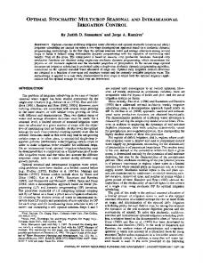
System Specification
Functional Design
Clock Tree Synthesis
Circuit Timing Information
Logic Design
Optimal Clock Skew Scheduling and Clock Delay Assignment
VLSI Circuit Design Cycle
Circuit Design
Circuit Design of the Clock Distribution Network Calculate Worst Case Path Delay Variation
Process Parameter Information
No
Increase Safety Term ζij
Clock Skew Schedule Violation ?
Yes Automated Layout
Upper Bound Violation ?
Fabrication
Increase the Clock Period TCP
Yes
Increase the Clock Period TCP
Yes No
Lower Bound Violation ?
No
Compensation for Process Variations
3. REDUCED TOLERANCE TO PROCESS PARAMETER VARIATIONS
Figure 6: Synthesis methodology of clock distribution networks tolerant to process variations
A top-down design methodology has been developed for synthesizing intentionally skewed clock distribution networks from the timing constraints of the circuit without prior layout information [7,9], as illustrated in Figure 6. The top-down synthesis methodology is integrated with a bottom-up verification phase (darker-shaded region in Figure 6) to ensure that the effects of process parameter variations on the selected clock skew values do not violate the bounds of the effective permissible range of each local data path. The clock distribution network is primarily composed of active devices (CMOS inverters) that accurately implement the clock path delays that enforce non-zero clock skew. The circuit modeling of the clock tree with active devices is based on the alpha-power law model [11]. Due to the active devices within the clock tree, the clock path delay variations are primarily due to the effects of process parameter variations on the active devices rather than variations of the interconnect lines within the clock tree [12]. Once the clock distribution network has been designed, each clock path delay is re-calculated assuming that the cumulative effects of device parameter variations, such as threshold voltage and channel mobility, can be collected into a single parameter characterizing the gain of a CMOS inverter, specifically the output current IDO [11]. The worst case variation of each clock skew is determined from calculating the minimum and maximum clock path delays considering the minimum and maximum IDO of each inverter within each branch of the clock distribution network. If a single worst case clock skew value is outside the effective permissible range of the corresponding local data path, TSkewij ⊄ ρ(Lij), a timing constraint is violated and the circuit will not function properly. This violation is passed to the top-down synthesis system, indicating which bound of the effective permissible range is violated. The clock skew of at least one local data path Lij within the system may violate the upper bound of ρ(Lij), i.e., TSkewij > TSkewij(max). This violation is corrected by increasing the clock period TCP, since due to monotonicity the effective permissible clock skew range for each local data path is also increased (TSkewij(max) is increased). The new clock skew value may also violate the lower bound of a local data path, i.e., TSkewij < TSkewij(min), where TSkewij(min) ⊂ ρ(Lij).
Two compensation techniques are used to prevent lower bound violations, depending on where the effective permissible range of a local data path ρ(Lij) is located within the permissible range of the local data path, Pl(Lij). If the lower bound of ρ(Lij) is greater than the lower bound of Pl(Lij), the clock period TCP is increased until the race condition is eliminated, since the effective permissible range will increase due to monotonicity. However, if after increasing the clock period, the clock skew violation still exists and the lower bound of the effective permissible range is equal to the lower bound of the local data path {MIN[ρ(Lij)] = MIN[Pl(Lij)]}, any further increase of the clock period will not eliminate the violation caused by not satisfying (1). Rather, if the lower bound of ρ(Lij) is equal to the lower bound of Pl(Lij), a safety term ζij > 0 is added to the local timing constraint that defines the lower bound of Pl(Lij), [see (1)]. The clock period is increased and a new clock skew schedule is calculated for this value of the clock period. The increased clock period is required to obtain a set of effective permissible ranges with widths equal to or greater than the set of effective permissible ranges that existed before the clock skew violation. Observe that by including the safety term ζij, the lower bound of the clock skew of the faulty local data path is shifted to the right, moving the new clock skew schedule of the entire circuit away from the bound violation and minimizing the likelihood of any race conditions. This iterative process continues until the worst case variations of the selected clock skews no longer violate the corresponding effective permissible ranges. 4. SIMULATION RESULTS The simulation results presented in this section illustrate the performance improvements obtained by exploiting non-zero clock skew while considering the effects of process parameter variations. In order to demonstrate these performance improvements, the suite of ISCAS-89 sequential circuits is chosen as benchmark circuits. The unit fanout delay model (one unit delay per gate plus 0.2 units for each fanout of the gate) is used to estimate the minimum and maximum propagation delay of the logic blocks. The set-up and hold times are set to zero. The performance results are illustrated in Table 1. The number of registers and gates within the circuit including the I/O registers are shown in Column 2. The upper bound of the clock period
assuming zero clock skew is shown in Column 3. The clock period obtained with intentional clock skew is shown in Column 4. The resulting performance gain is shown in Column 5. The clock period obtained with the constraint of zero clock skew imposed among the I/O registers is shown in Column 6 while the performance gain with respect to a zero skew implementation is shown in Column 7. Table 1: Performance improvement with non-zero clock skew circ. ex1 s27 s298 s386 s444 s510 s838
size #reg./#gates 20/7/10 23/119 20/159 30/181 32/211 67/446
TCPo TSkewij = 0 11.0 9.2 16.2 19.8 18.6 19.8 27.0
TCPi TSkewij ≠ 0 6.3 5.4 11.6 19.8 11.1 17.3 13.5
gain (%) 43 41 28 0 41 13 50
TCP TSkewI/O = 0 7.2 6.2 11.6 19.8 11.1 17.3 15.6
gain (%) 35 33 28 0 41 13 42
The results shown in Table 1 clearly demonstrate reductions of the minimum clock period when intentional clock skew is exploited. The amount of reduction is dependent on the characteristics of each circuit, particularly the differences in propagation delay between each local data path. Note also that by constraining the clock skew of the I/O registers to zero, circuit speed can be improved, although less than without this constraint. Examples of clock distribution networks which exploit intentional clock skew and are less sensitive to the effects of process parameter variations are listed in Table 2. The clock trees are synthesized with the methodology presented in [7,9]. The clock skew values are derived from a circuit simulation of the clock path delays of a clock tree using SPICE Level-3 assuming the MOSIS SCMOS 1.2 µm fabrication technology. The minimum clock period assuming zero clock skew TCPo and intentional clock skew TCPi is shown in Column 2, respectively. The permissible range most susceptible to process parameter variations is illustrated in Column 3. The target clock skew value is shown in Column 4. In Columns 5 and 6, respectively, the nominal and maximum clock skew are depicted, assuming a 15% variation of the drain current IDO of each inverter. Note that both the nominal and the worst case value of the clock skew are within the permissible range. The per cent variation of clock skew due to the effects of process parameter variations is shown in column 7. A 20% improvement in speed with up to a 30% variation in the nominal clock skew, and a 33% improvement in speed with up to an 18% variation in the nominal clock skew are observed for the example circuits listed in Table 2. Table 2: Worst case variations in clock skew due to process parameter variations, IDO = 15% circuit TCP0/TCPi permissible selected range clock skew cdn 1 cdn 2 cdn 3
11/9 18/15 27/18
[-8,-2] [-6.8, -1.4] [-14, 2.3]
-3.0 -4.2 1.1
Simulated skew (ns) nom worst case -3.0 -2.10 -4.1 -3.3 1.14 1.3
Error (%) nom 0.0 2.4 3.6
worst case 30.0 21.4 18.2
5. CONCLUSIONS The problem of scheduling clock path delays such that intentional localized clock skew is used to improve performance and reliability while considering the effects of process parameter variations is examined in this paper. A graph-based approach is presented for determining the minimum clock period and the
permissible ranges of each local data path. The process of determining the bounds of these ranges and selecting the clock skew value for each local data path so as to minimize the effects of process parameter variations is described. Rather than placing limits or bounds on the clock skew variations, this approach guarantees that each selected clock skew value is within the permissible range despite worst case variations of the clock skew. The clock skew scheduling algorithms for compensating for process variations have been incorporated into a top-down, bottom-up clock tree synthesis environment. In the top-down phase, the clock skew schedule and permissible ranges of each local data path are determined to allow the maximum variation of the clock skew. In the bottom-up phase, possible clock skew violations due to process parameter variations are compensated by the proper choice of clock skew for each local data path and the controlled increase of the clock period TCP. The clock period of a number of ISCAS-89 benchmark circuits are minimized with this clock scheduling algorithm. Scheduling the clock skews to make a clock distribution network more tolerant to process parameter variations is presented for several example networks. The results listed in Table 2 confirm the aforementioned claim that variations in clock skew due to process parameter variations can be both tolerated and compensated. 6. REFERENCES [1] J. P. Fishburn, “Clock Skew Optimization,” IEEE Transactions on Computers, Vol. C-39, No. 7, pp. 945-951, July 1990. [2] E. G. Friedman, Clock Distribution Networks in VLSI Circuits and System, IEEE Press, 1995. [3] K. A. Sakallah, T. N. Mudge, O. A. Olukotun, “checkTc and minTc: Timing Verification and Optimal Clocking of Synchronous Digital Circuits,” Proceedings of the IEEE/ACM Design Automation Conference, pp. 111-117, June 1990. [4] T. G. Szymanski, “Computing Optimal Clock Schedules,” Proceedings of the IEEE/ACM Design Automation Conference, pp. 399-404, June 1992. [5] N. Shenoy and R. K. Brayton, “Graph Algorithms for Clock Schedule Optimization,” Proceedings of the IEEE International Conference on Computer-Aided Design, pp. 132-136, November 1992. [6] R. B. Deokar and S. Sapatnekar, “A Graph-theoretic Approach to Clock Skew Optimization,” Proceedings of the IEEE International Symposium on Circuits and Systems, pp. 407-410, May 1994. [7] J. L. Neves and E. G. Friedman, “Design Methodology for Synthesizing Clock Distribution Networks Exploiting Non-Zero Localized Clock Skew,” IEEE Transactions on VLSI Systems, June 1996 (in press). [8] D. G. Messerschmitt, “Synchronization in Digital System Design,” IEEE Journal on Selected Areas in Communications, Vol. 8, No. 6, pp. 1404-1419, October 1990. [9] J. L. Neves, Synthesis of Clock Distribution Networks for High Performance VLSI/ULSI-Based Synchronous Digital Systems, Ph.D. Dissertation, University of Rochester, December 1995. [10] E. L. Lawler, Combinatorial Optimization: Networks and Matroids, Holt, Rinehart and Winston, 1976. [11] T. Sakurai and A. R. Newton, “Alpha-Power Law MOSFET Model and its Applications to CMOS Inverter Delay and Other Formulas,” IEEE Journal of Solid State Circuits, Vol. SC-25, No. 2, pp. 584-594, April 1990. [12] M. Shoji, “Elimination of Process-Dependent Clock Skew in CMOS VLSI,” IEEE Journal of Solid State Circuits, Vol. SC-21, No. 5, pp. 875-880, October 1986