Email {sbae, mangalag, vijay}@cse.psu.edu ... Abstract - Clock skew scheduling (CSS) is an effective ... design structural constraints that affect the CSS and.
Exploiting Clock Skew Scheduling for FPGA Sungmin Bae, Prasanth Mangalagiri, N. Vijaykrishnan Email {sbae, mangalag, vijay}@cse.psu.edu CSE Department, Pennsylvania State University, University Park, PA 16801, USA Abstract - Clock skew scheduling (CSS) is an effective technique to optimize clock period of sequential designs. However, these techniques are not effective in the presence of certain design structural constraints that limit the CSS. In this paper, we present an analysis of several design structural constraints that affect the CSS and propose techniques to resolve these constraints. Furthermore, we propose a CSS FPGA architecture and a novel clock-period optimization (CPO) flow that tackles some of these constraints by exploiting the reconfigurability of FPGAs. Experimental results demonstrate that the proposed FPGA architecture with the CPO flow achieved an average performance improvement of 24.4% which was an average performance improvement of 10.7% over the CPO flow without considering the constraints.
I.
INTRODUCTION
FPGAs are increasingly preferred over ASICs in various domain specific applications due to short timeto-market, easy verification, and low non-recurring costs. However, the relatively slow speeds of FPGAs when compared to ASICs, have led to efforts targeted to improve performance at various levels of the design flow. Among them, clock skew scheduling (CSS) is a technique that optimize clock period of circuits in a post place and route phase [1] [2] [3] [4]. Ideally a CSS optimizes clock period of a design to an average delay of pipeline stages from a primary input to a primary output, instead of the slowest pipeline stage delay. However, the amount of optimization can be limited by several design structural constraints such as unbalanced paths, fixed clock skew in external flip flops, self loop paths and finite clock skew range and granularity. Ignoring these constraints could result in achieving a sub-optimal improvement in timing from clock-period optimizations. There have been several studies that implement a clock skew scheduling technique on an FPGA. In [1], the authors use global clock lines to carry skewed clock signals to optimize clock period of sequential circuits. There are various advantages to this method. It incurs no hardware overhead and numerous combinations of skew values can be carried on the clock lines. However, this technique could result in considerable power consumption overheads, since skewed clocks are carried over global clock lines. Furthermore, skew values are limited to the available global clock lines. In [2], the authors use a clock architecture composed of a
978-3-9810801-5-5/DATE09 © 2009 EDAA
global H-tree and a local row based routing technique. They control the clock-skew by inserting programmable delay elements (PDE) at the root and branch points of the H-tree. Such a hierarchical placement of PDEs in the clock tree results in a wider range of global skew values. However, the range of clock skew is limited when two nodes share the same parent node. Hence the range of skew values achieved by hierarchical PDE based clock tree is limited by the placement of the nodes. Also today’s FPGAs have multiple global clock trees, placing PDEs at the branches of each of the clock trees can lead to large hardware overheads. Authors in [2] also propose skewflexibility aware placement algorithms which relax timing constraints during placement to increase solution spaces of placement, and use clock-skew scheduling to compensate for any possible increase in critical path delay. However, all the above approaches do not address some of the key structural constraints that limit the achievable clock period optimization for a given design. The paper is organized as follows. In section 2 we discuss the basic concepts of clock-skew scheduling. In section 3 we discuss in detail various design-based structural scenarios that limit the clock period optimization and techniques resolve such limitations. Section 4 and 5 present our clock skew scheduling FPGA architecture and a novel clock period optimization CAD flow that take in to consideration the various design limitations during post-layout clock period optimization, and discuss in detail the various phases involved. Section 6 discusses the achieved clock period optimizations results and section 7 concludes the paper. II.
CLOCK SKEW SCHDEULING
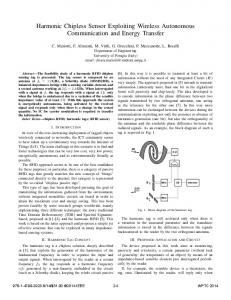
In general, the clock period of a design is decided by its critical path delay. However, using clock skew scheduling techniques the clock period of a design can be optimized to improve performance. Timing Constraints Fig. 1 depicts paths through combinational logics between a source and sink flip flop (FF) pair, FFj and FFk respectively. Since there are no sequential elements between this pair of FFs, they can be classified as
sequentially-adjacent [3]. Sj and Sk indicate clock skew from the clock source at FFj and FFk. Dmax (j, k) and Dmin (j, k) denote the maximum and minimum combinatorial path delay between the sequentiallyadjacent pair of FFj and FFk, respectively. CP, Tsetup and Thold denote the clock period, setup and hold time of the FFs, respectively. Sj denotes the clock skew value at flip-flop FFj. The two key timing constraints that must be satisfied in clock skew scheduling, by every source and sink FF pairs for successful operation of sequential circuits are as follows. Dmax (j, k) < CP + Sk – Sj – Tsetup
(EQ 1)
Dmin (j, k) > Thold + Sk – Sj
(EQ 2)
The data signals propagating from FFj in the nth clock cycle towards FFk, must arrive at least Tsetup time before the (n+1) th clock edge of FFk for successful sampling. This constraint also known as zero clocking constraint is depicted in equation 1. In the presence of clock skews there can be a scenario in which the data signals from the source flip-flop (FFj) arrive at the sink too early and disappear before being sampled due to the clock skew (Sk) at FFk. This constraint also known as double clocking constraint is depicted in equation 2. To avoid “data race” conditions the arrival time of the data signals must be Thold after the nth clock edge of FFk. The CSS [4] involves finding the minimum clock period at which all the sequentially adjacent FFs of the circuit satisfy the timing constraints show in equations 1 and 2.
Dmin value of 1ns obtained from path 2 limits the extent of clock skew at FFk to 1ns. Such a low skew value at FFk limits the amount of slack that can be borrowed by paths 1 and 3 which in turn limits the improvement in clock period. Therefore, the presence of unbalanced paths in a design can lead to sub-optimal solutions to the CSS problem. Balancing Path Delays Fig. 2 depicts a scenario where partial re-routing of paths can resolve an unbalanced path delay incurring timing constraint violation. We assume that the design needs to be optimized to achieve a clock period of 7ns, with the maximum clock skew value as 5ns and initially all route delays are zero. It can be observed that the path from FF1 to FF2 violates a zero clocking constraint. A 2ns more slack has to be borrowed by either decreasing or increasing the clock skews at source and sink FFs respectively. However, the maximum clock skew value of 5ns limits any increase to the CS of FF2. Hence, the CS value of FF1 needs to be decreased by 2ns without violating the constraints of any related paths. It can be observed that reducing CS at FF1 to 1ns does not cause the zero clocking constraint violation for FF1 and FF3 pair. However, it causes a double clocking constraint violation for the path between FF1 and FF4. With CS of FF3 being zero, to avoid a zero clocking constraint violation between FF3 and FF4, the CS of FF4 cannot be decreased. In such a scenario, by finding an alternate route which increases the path delay between FF1 to LB4 by 1ns we can achieve the desired clock period; the increase in the path delay can be achieved through partial re-routing in the FPGA. Also the effect of increased resistances and capacitances of the route to other paths in the net can be isolated using the routing buffers in the FPGA.
Fig. 1. Timing Constraints
III.
DESIGN CONSTRAINTS LIMITING CLOCK PERIOD OPTIMIZATION AND TECHNIQUES RESOLVING THE CONSTRAINTS
In this section, we analyze some of these key design structural constraints that limit the clock period optimization (CPO) in FPGAs and discuss techniques to enhance clock skew optimization from the constraints. A. Unbalanced Path Delays Minimum clock period of a sequentially adjacent FF pair is dependent on the difference between the Dmax and Dmin of the pair [4]. The clock skew assignment at the sink FF should be less than Dmin, to satisfy the double clocking constraints (assuming zero clock skew at the source FF). In example depicted in Fig. 1, the
Fig. 2. Path Balancing
B. Fixed Clock Skew of External FFs FFs located at a chips I/O have a fixed clock skew to enable communication with external devices. Such FFs having a fixed clock-skew are known as external FFs. On the other hand FFs that can be skew-controlled are known as internal FFs. Fixed clock-skew for external communication could be a limitation to the clock period optimization.
Donor FF Insertion A donor FF is a dummy FF used only to provide additional slack in its path. Fig. 3 depicts a scenario where clock period optimization is not possible due to a fixed CS value of zero at the external FF. However, by inserting a donor FF in the path between the external FF and Logic Block (LB) 2, a 3ns slack can be borrowed decreasing the CP value to 4ns. Note that donor FFs should be inserted so that there are no logic blocks between the donor FFs and the external FFs. This is necessary to not alter the functionality of the design. It can be observed that donor FF insertion at the external FFs increases the pipeline depth of the design by a single level. Therefore, the insertion can result in increasing the latency of the design if the clock period reduction achieved does not compensate for the increase in pipeline depth.
path to borrow slacks results in reducing slacks of the feedback loop. Fig. 4c depicts such a scenario where the skew optimization of two FFs belonging to different clock skew clusters is limited by their individual CS values.
Fig. 4. Self loop paths (a) Single FF loop (b) LUTs sharing a single CSCB cluster (c) LUTs across CSCB clusters
CSS Aware Clustering and Placement Algorithm
Fig. 3. Donor FF insertion
C. Self Loop Paths The data paths in a circuit that originate at a FF output and have a feedback loop through combinatorial logic are termed as self-loop paths. The simplest case of self loop paths (Fig. 4a) occurs when the source and sink FF are the same. In this case the minimum clock period is the Dmax of the path itself. Due to the feedback loop, assigning clock skew at the FF has no effect. Hence there is no scope to optimize the clock period by borrowing slack from the faster paths. Therefore, the optimized clock period must be above the self-loop path delay. In essence, the self-loop path constraint decides the set of path delays to be averaged by CSS. The second case, depicted in Fig. 4b, occurs depending on the granularity of clock skew controlling blocks. Since implementing a clock skew control block at the granularity of each FF is prohibitive due to huge hardware overhead, several FFs have to be grouped together. This clustering can cause the same effect as self looping for a single FF. In this case, both the source and sink FFs are placed in the same cluster, and can only be assigned a single clock-skew value. In the third case of self loop paths, we take into consideration FFs that not only belong to a single skew control cluster but also FFs that pan across different skew cluster blocks. This design constraint occurs when a group of FFs are in a circular feedback loop. In such cases increasing clock skew of FFs in forward
The self loop path constraints could be resolved by CSS aware clustering, placing and routing algorithms that optimize the timing of self-loop paths. These algorithms may increase the critical path delay of a design. However, CSS may further optimize the clock period of a design without self-loop paths limitation. Also [2] reported that additional 21% performance improvement was observed by using their skew flexibility aware quadratic placement algorithm. D. Finite Clock Skew Range and Granularity Implementing clock skew scheduling on FPGAs requires pre-built clock skew control blocks. The granularity and the range of clock skews achieved by the control blocks play an important role in achieving an optimal clock skew schedule. However, the skew range and granularity of a block can only have finite values as the clock skew control logic is implemented using a chain of inverters and the number of these blocks and inverters are fixed during the design of the FPGA. Fig. 5a demonstrates a scenario, assuming no other limitations exist for the optimization, where a maximum clock skew range of 2ns at FF2 limits the optimized clock period only to 5ns. It can be observed that by increasing the maximum clock skew range to a 3ns clock skew at FF2 can decrease to 4ns, the clock period. Fig. 5b shows a scenario where a minimum clock skew value of 2ns at FF2 prevents the clock period optimization. It can be observed that by decreasing the minimum skew value to 1ns clock skew at FF2 can reduce the clock period from 7ns to 6ns. Find Optimal Clock Skew Range and Granularity The clock skew range and granularity of a CSCB are decided by the domain knowledge of designs configured on a FPGA. Since, the clock skew block needs to cover a wide range of their critical path delays,
in order to achieve the desired performance optimization. Therefore, the decision of the clock skew range and granularity has dependence on the speed and size of a FPGA, which decide the range of critical path delay of designs to be implemented on the FPGA. However, covering a wider range of clock skews with a finer granularity of skew values might increase hardware overheads. Therefore, careful design considerations are required to find an optimal range and a granularity in terms of the both average performance improvement and the incurred area overhead.
CSCBs at the branches each of the clock trees can lead to large hardware overheads. Hence, in our architecture we place a single CSCB in every CLB. As shown in Fig. 6b, output of a CSCB, which is a skewed clock signal, is connected to all the FFs in a CLB. B. Clock Skew Enabled I/O Architecture The external FFs located at a chip I/O are not allowed to have an intentional clock skew to enable communication with external devices. In order to resolve the fixed clock-skew constraint, we propose clock skew enabled I/O elements (IOE) in the FPGA. To enable clock skew at the IOE, donor FFs and a CSCB are required at each IOE. However, with little modification on an IOE, this can be achieved without incurring large area overhead for a recent FPGA. Fig. 7a shows a simplified schematic of bidirectional I/O element (IOE) of the Stratix IV FPGA, which contains built in programmable delay units in both input and output paths of the IOE. The clock skew enabled I/O can be designed adding donor FFs at the input of output path (Data path of FPGA to external devices) and utilizing the inactive programmable delay unit at the input path (Data path of external devices to FPGA) as a CSCB. In addition, MUXs are added to control usage of the donor FFs. (See Fig. 7b)
Fig. 5. (a) Effect of finite maximum skew range (b) Effect of finite minimum skew value
IV. FPGA ARCHITECTURE FOR CLOCK SKEW SCHEDULING Implementing the clock skew scheduling on FPGAs requires techniques that are different from the ones used in ASICs. In this section, we discuss the various factors to be taken into consideration, during the design of a clock skew scheduling FPGA architecture. Fig. 7.
A. Clock Skew Control Block Architecture
(a) Simplified Schematic of Original IO Element [10] (b) Clock Skew Enabled IO Element
C. Hardware Overheads In this section we evaluate the area overheads, due to the additional clock skew logic used in our FPGA architecture. Fig. 6.
(a) Clock Skew Control Block (CSCB) (b) A CLB with CSCB
Our Clock Skew Control Block (CSCB) architecture, shown in Fig. 6a is similar to that of a PDE described in [2]. The output MUX of a CSCB selects varying number of skew elements implemented using a chain of inverters, based on the value in the memory cell of the control unit. Thus CSCBs can provide a range of clock skew values. In [2] the authors suggest placing PDEs at every branch of a global clock tree to achieve hierarchical range of skew values. However, since FPGAs have multiple global clock trees, placing
To determine the range and granularity of clock skew value we ran experiments on benchmark designs by varying the maximum skew range and the number of skew elements for a maximum skew range value. The skew range of about 25% of critical path delay of the slowest design and dividing the range to 8 skew levels was optimal in terms of the both average performance improvement and the incurred CLB area overhead. However, this result may vary with benchmarks used. From the result above, each CSCB has 7 skew elements in a CSCB supporting 8 different clock skew
values ranging from 0 to 7. The delay levels are achieved by a skew element containing 12 inverters. Three memory cells and a MUX are used to control the amount of skew values. We estimated the area overhead of CLB based on the resources used by the eight 6-input LUTs of VPR’s CLB architecture from the number of minimum sized transistors used. The clock skew control block increases the area of a CLB by 6.6 %. However, it is well known that the routing logic dominates the area of an FPGA. If we assume an FPGA in which CLBs account for a 25% of the total chip area, then the clock skew logic has only 1.65% area overhead of the FPGA. Accurately quantifying the overhead of clock skew enabled IOE is challenging due to lack of detailed information about the IOE architecture. However, based on [10], the number of additional FFs and MUXs are counted as less than 10% of the original number of FFs and MUXs in the IOE. Furthermore, considering other units, such as programmable delay units, input and output buffers, programmable pull-up resistor, and a bus-hold circuit etc, we believe that the area overhead of the modified IOE will be much less than 10% of original IOE. Pessimistically assuming, MUXs and FFs occupy 50% of an IOE area, and IOE takes 20% of FPGA area, the area overhead is about 1.0% of the FPGA. From the overhead estimations above, the overall area overhead of the proposed FPGA architecture is expected to be about 2.7%.
IOE are enabled. And if the violations are caused by unbalanced paths, we calculate the required delay amount of the paths to the Path Balancing Phase to find an alternative route satisfying the timing constraints. Our heuristic-based path balancing algorithm is as follows, when the extent of clock skew variation to satisfy zero clocking constraints is limited by double clocking constraints at FFs, the double clocking constraints are solved by increasing path delays, if the increase in the path delay does not cause zero clocking constraints to other paths. To achieve such an increase in path delay in our CPO flow, we augment the routing algorithm in versatile place and route (VPR) [7]. The desired path delay, along with the routing information of source and sink FF pairs and all other paths information are given as input to the router. Then all possible routes between the FFs are explored till the desired increase in delay is achieved.
V. CLOCK PERIOD OPTIMIZATION (CPO) FLOW We present a novel clock skew scheduling tool flow that takes in to consideration the design constraints, namely unbalanced path delays and fixed clock skew at external FFs among all the constraints, and achieves an enhanced performance improvement by exploiting the re-configurability of FPGAs; constraints due to selfloop paths have to be resolved at clustering, and place and route phases of the design flow and finite skew range constraints have to be handled at design phase of the FPGA. In this work, since we perform CPO at postplace-and-route phase we target constraints due to unbalanced paths and fixed clock skew at external FFs. In future, we plan to extend our CPO flow to the clustering and place and route phases of the design flow. Fig. 8 depicts the control flow of our CPO Flow. The flow starts with a binary search based Clock Skew Scheduling (CSS) phase to find minimum clock period (CP) that satisfies the timing constraints with input as the Dmax and Dmin values of all the sequentially adjacent FF pairs. We focus on the set of FF pairs which have violated the timing constraints causing CSS to fail. We then analyze the failed timing constraints to extract any design constraints that has to lead the failure for the failed CP values, which is closest to the minimum CP value determined by the CSS. If the violations are caused due to the fixed slack of external FFs in the causal FF pair, then the donor FFs in the
Fig. 8. Clock Period Optimization Flow
VI. EXPERIMENTAL RESULTS In this section we present the CPO flow experimental results obtained from several large benchmarks selected from MCNC and ISCAS-89 benchmark suites will be presented. Versatile place and route (VPR) [6] was used to perform placement and routing, and calculate path delays. MicroMagic’s MAX Layout editor was used to layout design components namely LUTs, CLBs, CSCB etc and HSPICE was used to calculate various architectural parameters (such as capacitance, resistance, delay and power consumptions etc) with 45nm PTM [7]. The benchmarks were configured in VPR’s island style FPGA architecture, with 6-input LUTs, and a cluster size of 8. Each benchmark is placed and routed on minimum sized FPGA and channel width. Routing segments are bidirectional and all length of 4 segments with tri-state buffer switches. And dynamic and leakage power consumption of CSCBs are estimated based on the Power-modeling FPGA [9], which considers a transition density and static probability of each node in a design, and is also modified to estimate leakage power based on input vector states on circuits.
The clock period improvements achieved by our CPO flow from benchmarks are shown in Table 1. The designs were analyzed after CSO to extract the design structural constraints limiting CPO. In designs having the fixed CS of external FFs as key the limiting factor, donor FF insertion achieved an average performance improvement of 13.5% over the traditional CSO flow. In case of designs where unbalanced paths were limiting factors, an average performance improvement of 6.17% over a traditional CSO flow was observed. However, CPO flow did not resolve the unbalanced path delay constraint for all designs. No alternate routes satisfying the timing constraint were found during the flow for tseng benchmark. Run times of the path balance algorithm on 1.8 GHz Intel Core Duo CPU with 2gigabytes of memory varied between 1~5mins. Our CPO flow achieves total performance improvement of 24.37% which was an average performance improvement of 10.68% over the CSO flow without the constraints consideration. The average CSCB power consumption of 0.97% of total FPGA power consumption was observed, which ranged from 0.6~1.9% depending on the number of skew elements used and the power consumption of the designs. If we increase the channel width to reflect actual FPGAs the CSCB power consumption portion will be decreased. While, the designs with the self-loop constraints had average total performance improvement of 16.9%; clock skew scheduling aware clustering and placement and routing algorithms are required to get more benefit from the CSS FPGA architecture. VII. CONCLUSION In this paper, we present an analysis of various design structural constraints that limit clock period optimization and techniques resolve the constraints. We also present our CSS FPGA architecture equipped with clock skew control blocks and clock skew enabled
IO elements. We then present our clock period optimization flow that takes into account the limitations due to unbalanced paths and fixed clock skew of external FFs constraints. Experimental results from benchmarks show that our CPO flow achieves total performance improvement of 24.37% which was an average performance improvement of 10.68% over the CSO flow without the constraints consideration. REFERENCES [1] Deshanand Singh and Stephen D. Brown, "Constrained Clock Shifting for Field Programmable Gate Arrays," International Symposium on FPGAs (FPGA.2002), Monterey, CA, Feb 2002, pp. 121-126. [2] Yeh, C. and Marek-Sadowska, M. 2005. Skew-programmable clock design for FPGA and skew-aware placement. In Proceedings of the 2005 ACM/SIGDA 13th international Symposium on FieldProgrammable Gate Arrays (Monterey, California, USA, February 20 - 22, 2005). FPGA '05. ACM, New York, NY, 33-40. [3] J. L. Neves et al., “Automated synthesis of skew-based clock distribution networks,” VLSI Design, vol. 7, No. 1, pp. 31-57, 1998. [4] John P. Fishburn, Clock Skew Optimization, IEEE Transactions on Computers, v.39 n.7, p.945-951, July 1990 [5] Ivan S. Kourtev, Eby G. Friedman, “Timing Optimization through Clock Skew Scheduling” Kluwer Academic Publishers. [6] Betz, V. and Rose, J. 1997. VPR: A new packing, placement and routing tool for FPGA research. In Proceedings of the 7th international Workshop on Field-Programmable Logic and Applications (September 01 - 03, 1997).
[7]
Zhao, W. and Cao, Y. 2006. New Generation of Predictive Technology Model for Sub-45nm Design Exploration. In Proceedings of the 7th international Symposium on Quality Electronic Design (March 27 - 29). [8] T.H Cormen, C.E. Leiserson, and R.L Rivest, Introduction to Algorithms, McGraw-Hill, 1990. [9] K.K.W. Poon, A. Yan, S.J.E. Wilton, ``A Flexible Power Model for FPGAs'', in 12th International Conference on FieldProgrammable Logic and Applications, Sept 2002. [10] Stratix IV Device HandBook Volume 1
Benchmarks
# of LUTS
# of FFs
bigkey clma diffeq elliptic frisc
1840 8384 1504 5040 4080
224 33 377 1122 886
Without the Constraints Consideration 22.58% 7.56% 28.04% 13.3% 12.11%
tseng
1056
384
27.75%
dsip s38584.1 s38417 s35932 s15850 s13207 s5378 Average
2664 6696 6408 5456 2024 2400 448
224 1259 85 1728 540 469 160
14.44% 16.52% 12.65% 0% 3.62% 0% 19.37% 13.69%
Donor FFs
Path Balance
Routing Increase
Total Improvement
CSCB Power Consumption
15.81% 4.52% N/A N/A N/A
6.16% N/A N/A N/A N/A
22 N/A N/A N/A N/A
44.54% 12.08% 28.04% 13.3% 12.11%
1.9% 0.65% 0.92% 0.7% 0.63%
N/A
0%
No Route Found
27.75%
1.15%
Unbalanced Path
0.012% 15.96% 15 30.41% 6.95% N/A N/A 23.47% N/A N/A N/A 12.65% 41.07% N/A N/A 41.07% 8.22% 6.98% 7 18.81% 21.403% 1.75% 3 23.14% 10.05% N/A N/A 29.42% 13.5% 6.17% 24.37% Table 1: Experimental Results of CPO Flow
1.16% 0.83% 0.59% 1.48% 0.73% 0.82% 1.1% 0.97%
External FFs, Unbalanced Path External FFs, Self-loop Path Self-loop Path External FFs External FFs, Unbalanced Path External FFs, Unbalanced Path External FFs
Design Constraints External FFs, Unbalanced Path External FFs, Self-loop Path Self-loop Path Self-loop Path Self-loop Path