Dec 21, 2006 - This paper presents a new methodology of automatic RTL code generation from coarse- ...... He is a program co-chair of CODES+ISSS_ 2006,.
Journal of VLSI Signal Processing 2007
* 2007 Springer Science + Business Media, LLC. Manufactured in The United States. DOI: 10.1007/s11265-007-0070-9
Optimized RTL Code Generation from Coarse-Grain Dataflow Specification for Fast HW/SW Cosynthesis HYUNUK JUNG System LSI Division, CAE Center, Samsung Electronics Co., Ltd., Gyeonggi-Do, South Korea HOESEOK YANG AND SOONHOI HA Department of EECS, Seoul National University, Seoul, South Korea
Received: 21 December 2006; Accepted: 20 March 2007
Abstract. This paper presents a new methodology of automatic RTL code generation from coarse-grain dataflow specification for fast HW/SW cosynthesis. A node in a coarse-grain dataflow specification represents a functional block such as FIR and DCT and an arc may deliver multiple data samples per block invocation, which complicates the problem and distinguishes it from behavioral synthesis problem. Given optimized HW library blocks for dataflow nodes, we aim to generate the RTL codes for the entire hardware system including glue logics such as buffer and MUX, and the central controller. In the proposed design methodology, a dataflow graph can be mapped to various hardware structures by changing the resource allocation and schedule information. It simplifies the management of the area/performance tradeoff in hardware design and widens the design space of hardware implementation of a dataflow graph. We also support Fractional Rate Dataflow (FRDF) specification for more efficient hardware implementation. To overcome the additional hardware area overhead in the synthesized architecture, we propose two techniques reducing buffer overhead. Through experiments with some real examples, the usefulness of the proposed technique is demonstrated. Keywords: 1.
HW/SW codesign, system level design, dataflow graph (DFG), RTL, VHDL
Introduction
System level design methodology gains considerable research attention as the design complexity and the time-to-market pressure increase for SoC design. In system level design, a system level specification is mapped to an optimal architecture in a systematic way and the mapping is evaluated before implementation for fast design space exploration. As a specification model in this paper, we are concerned with a coarse-grain dataflow model that is adopted in many high level design frameworks [1–4], especially
for signal processing and multimedia applications because of formality and readability. In a dataflow graph G(V,E) as shown in Fig. 1a, an atomic node represents a coarse grain functional block such as FIR filter and DCT, and an arc represents the flow of data samples between two end nodes. When a node is invoked, it consumes the specified number of data samples from each input arc and produces the specified number of samples to each output arc. We use a rather restricted dataflow model, synchronous dataflow (SDF) [5] and its extension to fractional rate dataflow (FRDF) [6], in
Jung et al.
1
A
1
4
1
B
1
1
C
1
1
D
Mapped to hardware
E
1
RCV1
1
4
1
4
1
B
a
1
C
1
SND1
b
hardware resources
B
B C C C C
c
time
C C C C
B C C C C
d
e
Figure 1. a An initial dataflow specification; b partitioned subgraph mapped to hardware; c fully-sequential, d fully-parallel, and e hybrid execution of a multi-rate graph.
which the number of data samples produced or consumed on an arc is fixed a priori. If the number, called a sample rate, may not be unity, the dataflow graph is called a multi-rate graph. In Fig. 1, node C can be invoked 4 times after node B is invoked once. This restricted semantics enables us to verify important system properties such as memory boundedness and termination, and to estimate the system performance statically. A coarse grain block has complex properties such as data sample rates, I/O timings, data types, and its internal states. This dataflow model is different from control/data flow graph (CDFG) [7] commonly used in behavioral synthesis where a node typically represents a basic operation such as add or multiply that can be implemented simply using combinational logic. We define some terminologies. An invocation of a node is called an instance of the node. A hardware implementation of a node is defined as a hardware resource associated with the node. A hardware component is a physical entity, such as FPGA or ASIC, that integrates all hardware resources associated with the mapped nodes. In the proposed design methodology, a coarse grain functional block is the mapping unit in hardware/software partitioning decision. We assume that functional blocks are library blocks written in C code for software implementation, synthesizable VHDL code for hardware implementation, or both. If a function block is given as a legacy IP block, we may need to add wrapper logic to make it behave as a dataflow node. After hardware/software partitioning is performed, the dataflow graph is partitioned into several graphs that are mapped to hardware or software components. Figure 1b shows an example subgraph
mapped to a hardware component augmented with the interface blocks at the subgraph boundary. Figure 2 shows the simplified HW/SW codesign procedure starting from the dataflow specification. It is assumed that the performance of a node on each processing element (PE, processor or hardware IP) is given in a Node-PE database which also contains the additional information needed for system design such as consumed area and I/O bit width. The initial dataflow specification is first partitioned and scheduled in our design methodology. The partitioning and scheduling is performed by mapping the dataflow nodes to the processing elements in a selected architecture, based on the performance and cost information of nodes. After the partitioning and scheduling is completed for the selected architecture, SW and HW codes are automatically generated and cosimulated to verify the system performance. If it is not satisfied, we go back to the architecture selection step to choose other PEs or architectures. It forms the design space exploration (DSE) loop. In order to accelerate this design loop, it is highly desirable to automate HW and SW code generation from the dataflow specification. This automatic code generation can save time for both coding and debugging. This paper focuses on the automatic hardware code generation step, which is highlighted in Fig. 2, aiming to accelerate the hardware design and verification. Since the invocation order, or schedule, of dataflow nodes and the required hardware resources are given from the partitioning stage, the hardware code generation problem is to allocate
Dataflow Specification Node-PE Performance DB
Architecture Specification
Partitioning/Scheduling
SW subgraph SW schedule SW C code generation
HW subgraph HW schedule HW VHDL code generation VHDL Code
C Code Cosimulation
System Performance Satisfied? YES System Prototyping Sy
Figure 2.
Proposed system design procedure.
NO
Optimized RTL Code Generation from Coarse-Grain Dataflow
64
Transpose 8x8
Figure 3.
64
8
DCT1D
8
64
Transpose 8x8
64 8
DCT1D
different from ours in that they mainly concern the core (SDF node) generation only while we are also considering the efficient control logic generation. Key contributions in this paper can be summarized as follows:
8
Dataflow specification of 2D DCT algorithm.
hardware resources from the library, and synthesize the interface logic between blocks and the control codes for appropriate clocking and signaling. We enforce the resulting hardware to preserve the dataflow semantics to make the design correct by construction. A multi-rate dataflow graph is very popular in multimedia applications. When synthesizing a hardware component from the multi-rate dataflow graph, we have additional degree of freedom in the design space: parallelism. Even though there have been several works of automatic hardware code generation from dataflow specification, they do not consider the degree of parallelism. There are two different approaches to date: one is fully sequential approach as shown in Fig. 1c [3, 8] where all instances of node C are executed sequentially, and the other is fully parallel execution as shown in Fig. 1d [9]. However, the proposed technique explores diverse hardware implementations to consider the performance/area tradeoff: for example a hybrid execution of Fig. 1e is also explored, which is not considered in the previous approaches. The hybrid execution is taken into account in [10] under schedule restriction. But, their focus is 8 16bit signals
8 1-dimensional DCT blocks
Transpose 8x8 matrix
64 16bit inputs
1. We automate the integration of HW library blocks from an algorithm specification in dataflow model. It enables fast design space exploration by automating the time-consuming and error-prone task of interfacing and integrating HW blocks. We synthesize the glue logics and the central controller to make the HW operate preserving the dataflow semantics according to the schedule information. Therefore, the generated hardware is correct by construction. 2. By separating the scheduling and HW code generation, we can implement diverse HW architectures from the given dataflow specification by simply changing the schedule and resource sharing information. It widens the design space of hardware implementation, compared with the previous approaches based on dataflow specification. 3. Since the major overhead which makes the efficiency of generated hardware inferior compared to the manually optimized hardware comes from buffer of SDF arcs, we reduce the buffer size and the control logic dedicated to buffer control by proposing shift-buffering and buffer sharing schemes. Then, the area of optimized hardware is close to hand-optimized hardware.
DCT1D DCT1D DCT1D DCT1D DCT1D DCT1D DCT1D DCT1D
8 1-dimensional DCT blocks
Transpose 8x8 matrix
a M U X
M U X
DCT 1D
FIFO with 64 buffers
DCT 1D
DCT 1D wr wr_ok
controller
DCT1D DCT1D DCT1D DCT1D DCT1D DCT1D DCT1D DCT1D
rd_ok rd
ctrl
ctrl
ctrl
Handshaking control signals
b Figure 4.
DCT 1D
Hardware architecture assumed in a Ptolemy0, b Meyr_s0, and c GRAPE0.
c
ctrl
Jung et al.
In the next section, we overview some related works with a motivational example. After we explain how to define a block in Section 3, we describe the proposed technique in details with examples in Section 4. In Section 5, hardware implementation of a fractional rate dataflow specification is explained for more efficient implementation. Two buffer reducing techniques are proposed in Section 6, followed by experimental results in Section 7. Section 8 concludes the paper with discussion on the remaining topics in this subject.
2.
Previous Work and Motivational Example
In order to achieve fast HW/SW cosynthesis, many works have been done to automate hardware implementation from high-level specification in an HDL(Hardware Description Language) or from software specification in C/C++. Behavioral level synthesis from HDLs has a rather long history but with only a limited success. Recently HW synthesis from C or C++ has been actively pursued [11–13] in the realm of ESL (electronic system level) design. While they mainly concern about implementation of a hardware block itself, our approach focuses on implementing the hardware structure in the system level using the predefined library blocks. Hardware synthesis from SDL specification [14, 15] has been developed for rapid prototyping. This approach is similar to ours in that it is developed for system level design. However, its specification model and application domain are different from ours. It uses asynchronously communicating processes and mainly targets on telecommunication systems while ours uses a dataflow model, SDF [5], targeting for multimedia applications.
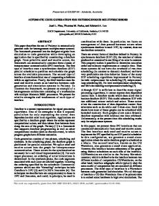
input
M U X
Figure 3 shows a dataflow graph of 2D DCT (discrete cosine transform) algorithm. It is a multirate dataflow graph with relatively high sample rates of 64 and 8. This algorithm can be mapped to various hardware implementations. A fully parallel implementation is taken in [9] by Ptolemy where eight resources of DCT1D block are created between two transpose blocks as shown in Fig. 4a. Note that eight DCT1D resources are activated at the same time after the transpose block produces 64 samples at once. And blocks are connected directly without buffer in-between. This parallel implementation results in the shortest processing delay but the largest hardware area, about 243,000 gates using 16 DCT1D resources in our experimentation. In Meyr_s approach [8, 16–18], the generated hardware structure has one-to-one correspondence to the dataflow graph where a separate hardware resource is allocated for each node. In Fig. 4b, one resource of DCT1D block is executed eight times sequentially to consume and produce 64 samples while one invocation of DCT1D block is assumed to consume eight samples at once1. If the DCT1D block is internally pipelined, eight invocations can also be pipelined. In this sequential implementation, a FIFO queue and a MUX are needed to accumulate 64 samples on the input and the output arcs of the transpose block respectively. But the hardware overhead is much smaller than that of parallel implementation. One difficulty of this approach is to generate numerous control signals whose timings are computed statically through rigorous graph analysis [17]. It has a serious restriction that all hardware blocks should have deterministic and fixed execution cycles for static timing analysis and controller synthesis. Another sequential implementation approach is taken by Ade et al. [3], Dalcolmo et al. [19],
M U X
DCT 1D
input
M U X
a Hardware architectures with a one 1D DCT resource and b four resources.
DCT 1D M U X
DCT 1D
controller Figure 5.
M U X
DCT 1D
controller
b
DCT 1D
SDF, FRDF
Shift buffering/buffer sharing N/A
SDF, CSDF, MDSDF SDF, CSDF
Static minimum
SDF Supported DFGs
SDF
N/A Buffer optimization
Port retiming
Centralized control
Variable Variable
Distributed control Distributed control
Variable Fixed Block execution time
Fixed
Centralized control Block control
Centralized control
Synchronous Asynchronous (FIFO) Asynchronous (FIFO) Synchronous Communication between blocks
Synchronous
Multiple/single/shared -resource allocation Multiple/single-resource allocation Single-resource allocation Multiple-resource allocation Resource allocation
Single-resource allocation
Parallel/sequential/hybrid implementation Parallel/sequential/hybrid implementation Sequential implementation Sequential implementation Parallel implementation Implementation of multi-rate specification
Meyr_s Ptolemy Approaches
Table 1.
Comparison among the approaches of HW synthesis from DFG.
GRAPE
McAllister_s
Proposed
Optimized RTL Code Generation from Coarse-Grain Dataflow
Lauwereins et al. [20] and in GRAPE system. Their approach is different from Meyr_s in that each hardware block has its local controller and there is no need of complicated central controller design (Fig. 4c). A hardware block detects when it can be invoked by exchanging the control signals with its neighbor based on a certain hand-shaking protocol. In this example, DCT1D block is sequentially invoked eight times after the transpose block produces 64 samples, repeatedly exchanging hand-shaking control signals per invocation. Thus, this asynchronous communication incurs non-negligible runtime overhead while it is robust enough to allow non-deterministic block execution time. The hardware overhead comes from the FIFO buffers inserted between the blocks and the local controllers. Distributed control and asynchronous communication of Fig. 4c are not commonly used in an optimized ASIC design. Figure 4a and b illustrate two extreme implementations of parallel and sequential operation. But, there are other implementation possibilities, some of which are displayed in Fig. 5. In Fig. 5a, a DCT1D resource is shared between two DCT1D nodes of Fig. 3. The DCT1D resource is invoked 16 times, 8 for column DCT and 8 for row DCT operation. It has the least amount of area with performance penalty. When better performance is required, the resources for column and row DCT are allocated separately and executed simultaneously in a pipelined fashion as already shown in Fig. 4b. In case the time constraint is tighter, more resources can be allocated as shown in Fig. 5b where two DCT1D resources are allocated to each DCT1D node. It is not fullysequential nor fully-parallel, so it is called a hybrid implementation. Such resource sharing and hybrid implementation are also taken into account in the proposed approach. Thus, the proposed approach widens the hardware design space considerably compared with the previous approaches based on dataflow specification. J. McAllister et al. [10] considered various implementations of a multi-dimensional SDF graph including hybrid implementation in targeting a reconfigurable device (e.g. FPGA). They assume asynchronous communication between nodes with a specific interface logic, called the Control and Communication Wrapper (CCW). Table 1 summarizes the comparison between these approaches. The proposed approach is unique in the following aspects: First, the scheduling and hardware
Jung et al.
clk rst
inputs
outputs
start
done
Figure 6. Input and output ports associated with a block with variable execution time.
synthesis is decoupled. Other approaches assume a fixed execution schedule of hardware components and synthesize the control logic to implement the schedule. On the other hand, a user may specify a schedule, and the hardware is automatically synthesized to implement the schedule in the proposed framework. Second, it uses a centralized controller for efficient implementation, but allowing variable execution length of hardware components. Buffer optimization on SDF arcs has been studied in Meyr_s and GRAPE group. By retiming technique, Horstmannshoff and Meyr [8] minimized number of the shimming registers between nodes. The lower bound of arc buffers was investigated by Ade et al. [21] in under data-driven execution. Some approaches support the extensions of SDF: CSDF [22] for GRAPE and McAllister_s, MDSDF [23] for Mcallister_s, and FRDF [6] for our approach. 3.
Block Types and Control Signals
In the proposed methodology, the complexity of a block definition is not restricted as long as the block follows the SDF semantics in which the block is triggered only when all input ports have enough data samples. It is important to note that the concept of a Bdata sample^ in the dataflow model is different from that of an Bevent^ that usually means the change of signal level on a wire. The arrival of a new sample should be notified by the predecessor block or by the controller based on the block schedule information. By preserving the SDF semantics in the generated hardware, we can guarantee the equivalence between the synthesized system and the dataflow specification in terms of functionality: So the
synthesized hardware is claimed to be correct by construction. To preserve the SDF semantics, we insert a buffer as a glue logic on every arc between two blocks. The buffer is latched with new output samples from the source block only after the block completes its execution. The destination block may read the valid data samples during the whole execution period. Thus the block needs no internal buffer to latch the input signal values. Buffer insertion strategy is also adopted in Sharp and Mycroft_s [24] work on SAFL language which specifies hardware behavior in a higher level abstraction. While they do not assume dataflow model, they observed that higher level structuring mechanism needs storage elements not wires in HW synthesis. The arc buffers are automatically generated and managed. The buffer management scheme is closely related with the types of blocks. We classify functional blocks into three different types based on the timing requirement of the internal behavior. The first type is combinational logic that does not include any internal register. Since we allow multi-cycle combinational logic, we compute the execution latency in terms of global clock cycles and trigger the output buffer load enable signal after the execution latency once the block is triggered by new input samples. The second type is a sequential logic with a fixed execution time. Since a sequential logic includes internal registers, three additional control signals (start, reset, and clock signals) are provided for the timing management of the internal registers. The reset signal is triggered in the initialization phase of the synthesized hardware. After the start signal is
clock start signal done signal Input valid timing output valid timing 2
3
4
5
6
7
8
9
10
counter
execution time • Start time = 3, End time = 8 • Execution time = End time – Start time + 1 = 6(cycles)
Figure 7.
An example timing diagram of the control signals.
Optimized RTL Code Generation from Coarse-Grain Dataflow
RCV
A
B
C
SND
Type A : combinational logic Type B : multi-cycle sequential logic with fixed execution time Type C : multi-cycle sequential logic with variable execution time
a en_a RCV
start signal start signal done signal clock en_b clock en_c reset reset
A
B start for B
clock
start for C
C done from C
Control signal generation logic
SND RCV start signal(B) A : 30
start signal(C)
B : 80
done signal(C)
C : Unknown
SND signal time
b Figure 8.
a An example DFG with various types of blocks, b synthesized hardware structure, and c the expected signal timings.
enabled, a fixed number of clock signals are counted to trigger the output buffer load enable signal. In case the minimum cycle time of a block is larger than the global clock period, the clock signal is obtained by down-sampling the global clock. The third type is a sequential logic with a variable execution time. Then we need another control signal, done, to indicate the completion of block execution: When the done signal is enabled, the output buffer load enable signal is triggered. Figure 6 shows the resultant input and output ports associated with this type of block and Fig. 7 illustrates an example of a timing diagram for the control signals. Since it is the most general type, it can be used for general legacy hardware IP. A third-party IP whose protocol is known to designer can be abstracted by the wrapper that translates IP specific protocol to this type. The
# resource allocation table Transpose 2 DCT1D 2 # resource mapping & schedule information # (instance name, resource number, start, duration) # loop ( loop count, start, loop period) Transpose_0 0 0 1 Loop 8 1 2 { DCT1D_0 0 0 2 } Transpose_1 1 17 1 Loop 8 18 2{ DCT1D_1 1 0 2 }
Figure 9.
c
Schedule information for the architecture of Fig. 4(b).
interrupt signal or a register value change that denotes the end of IP execution, for example, can be translated into the assertion of done signal. In this way, the proposed framework allows the use of legacy hardware IP blocks as long as there are corresponding dataflow nodes in the initial specification. Figure 8a shows a simple example that consists of all three types of blocks. The block types should be explicitly specified by the designer. Then the glue logics between blocks and the central controller are automatically synthesized, and integrated with the library blocks to result in the final architecture as shown in Fig. 8b. The design of controller is explained in the next section. In Fig. 8c the expected timing of control signals is drawn. Here, we assume that execution times of blocks A and B are 30 and 80 time units respectively, while the execution time of node C is unknown; the timing of done signal for block C is determined at run-time. The proposed technique discussed in this section can be summarized as follows: 1. Two adjacent blocks are communicated with each other through arc buffers. So the communication between blocks is managed simply by defining the timing of the buffer control signals. However, it implies that we add a buffer between two combinational logic blocks. Such extra buffer can be reduced by post-optimization phase in the proposed methodology, which will be discussed in Section 6. 2. The start signal is triggered to a sequential logic only after all input buffers complete latching of new data samples to satisfy the SDF semantics. If
Jung et al.
a block has multiple input arcs, it may lengthen the critical path length of a block. Relaxing the strictness of the SDF semantics for performance optimization is a future research subject. 3. The data samples on the input buffers remain valid at all times so that no internal buffering to latch the input signals is needed inside the block. 4.
Proposed Hardware Synthesis Technique
1 (Loop0)
8 (Loop1) Transpose_0
DCT1D_0
8 (Loop2) Transpose_1
DCT1D_1
Figure 10. Schedule information as a tree form: Leaf nodes and internal nodes stand for the nodes and loop iteration numbers respectively.
4.1. Schedule Information Structure for H/W synthesis The schedule information is obtained from the partitioning step in the proposed approach. Figure 9 shows an example schedule information for the architecture of Fig. 4b. The schedule information consists of two parts. One is resource allocation table and the other is mapping/schedule information. Resource allocation table is simply a set of pairs, {resource type name, number of resources}. There are two resources of transpose blocks and two of DCT1D blocks in Fig. 9. Mapping/schedule information defines the timing information of each instance of nodes. It also defines the allocated resource to the instance. It may be grouped by a loop to make a hierarchical representation. The syntax of the schedule information can be concisely represented by the following Backus Naur form (BNF) representation.
For example, Btranspose_1 1 17 1^ indicates that transpose_1 node uses the second resource (resource number=1) between two transpose resources and its start timing is 17. If a designer wants to generate a hardware structure like Fig. 5a, where two DCT1D blocks shares one hardware resource of DCT1D, he or she only has to modify the number of DCT1D resource to 1 and the mapped resource number of DCT1D_1 instance to 0 as follows. DCT1D 1 DCT1D_1 0 0 2 It means that only one DCT1D resource is allocated and all eight instances of DCT1D_1 node are also mapped to this resource. The time unit used to specify the start time and execution length is a clock cycle.
::= ::= set of ::= ::= set of ::= | < loop mapping_schedule> ::= ::= loop { }
Optimized RTL Code Generation from Coarse-Grain Dataflow
Loop0 Counter
Loop1 Counter
Loop2 Counter
Loop1 IterNum
Loop2 IterNum
done signal from the block. Then, the parent loop should check the done signals of the child loops with variable execution time recursively. Figure 13 shows an example in which Loop0 checks the done signals of Loop1 and Loop2 at their expected end times. If a done signal is not enabled, the counter waits until it is enabled. 4.3. Buffer Allocation
Figure 11.
Hierarchical loop control structure.
The schedule information in Fig. 9 contains two schedule loops. Since each loop has a local counter, the start time of the first block in a loop is set to 0. Loop 8 1 2 {DCT1D_0 0 0 2 } means that all eight instances of DCT1D_0 node use the first hardware resource of DCT1D and the resource is executed eight times consecutively with execution time equal to two cycles. Note that the repetition period is two while the loop starts at one. The schedule information associated with a DCT1D block of Fig. 5b can be represented as Loop 4 1 2 {DCT1D_0 0 0 2, DCT1D_0 1 0 2}. It means that first, third, fifth, and seventh instances are mapped to the first resource and the others are to the second resource. The entire schedule is also regarded as a loop since DFG is repeatedly executed as an infinite loop. 4.2. Counter-based Controller The schedule information of Fig. 9 can be organized as a tree data structure as shown in Fig. 10. Since the entire schedule is regarded as a loop, Loop0 is used for top-level control with loop count equal to one and the others are numbered in sequence. We synthesize the loop control hardware structure in the same fashion as the schedule data structure. As shown in Fig. 11, a loop counter is allocated for each loop and an iteration number counter is created for nested loops in order to count the loop iterations. Each loop counter and iteration number counter are controlled by their parent counter. The timing diagram in Fig. 12 shows the relationship among the counter values. Loop1 counter starts when Loop0 counter value becomes 1. The counter value increases by 1 at every clock cycle and Loop1 iteration number counter increases at the end of an iteration of Loop1. In case a loop contains a block that has varying execution time, the loop counter is stalled at the end of scheduled time of the block until it receives the
In the proposed technique, buffers between dataflow nodes are automatically allocated and connected to hardware resources. It should be noted that each port of dataflow hardware block may consume and produce multiple data samples at once. Consider a simple example in Fig. 14a. If we use only one hardware resource for each node, the schedule may be AABAB or (3A)(2B) where (3A) means A block is executed three times consecutively. In case the schedule is AABAB, the minimum required buffer size on the arc becomes four. If we use a looped schedule of (3A)(2B), the minimum required buffer size is increased to six. The relationship between scheduling and buffer size has been addressed in many researches [25] for software code generation. Buffer size requirement is also a key factor for hardware code generation. If we use maximum hardware resources for parallel execution using three resources for A and two resources for B in the example of Fig. 14a, the required buffer size should be six. Figure 14c illustrates buffer allocation and signal connection between buffers and blocks in this case. The required buffer size in case of maximum parallel execution becomes total number of sample exchange (TNSE) of the arc [25]. Given an dataflow arc a, we denote the source node and sink node of a by src(a) and snk(a) respectively. Also, p(a) and c(a) denote the number of data samples produced onto a by src(a) and consumed from a by snk(a) respectively. Then, TNSEðaÞ ¼ qðsrcðaÞÞ � pðaÞ ¼ qðsnkðaÞÞ � cðaÞ
Loop1_IterNum
0
1
2
3
4
5
6
ð1Þ
7
Loop1_Counter
0 1 0 1 0 1 0 1 0 1 0 1 0 1 0 0
Loop0_Counter
0 1 2 3 4 5 6 7 8 9 10 11 12 13 14 15 16 17
Figure 12.
Timing diagram of loop control counters.
time
Jung et al.
constant Last_CounterValue : integer := 34; … Loop0_counter : process(clock, reset) begin if reset = '1' then CounterValue