AbstractâWe propose a parallel implementation of the Cell. Average Constant False Alarm Rate (CA-CFAR) algorithm in reconfigurable hardware. The design ...
1
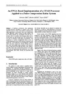
Parallel FPGA Design of CA CFAR Algorithm V.Kyovtorov, G.Kuzmanov, H.Kabakchiev, and G.Gaydadjiev
Abstract—We propose a parallel implementation of the Cell Average Constant False Alarm Rate (CA-CFAR) algorithm in reconfigurable hardware. The design is based on a parallel processing scheme employing extensive data reuse and synchronized sliding windows over the input data sequence. A scalable parallel structure is designed and mapped on Xilinx Virtex II Pro technology. Synthesis and post place and route results from the Xilinx ISE toolset suggest a linear speedup and resource utilization. More specifically, a single CFAR implementation utilizes 1.4% of the VIRTEX II Pro XC2VP30 chip, providing a throughput of 974 Mbps. Regarding the parallel design, a structure of 32 CA-CFARs provides 37.5% utilization and 31Gbps for the same FPGA chip. Furthermore, the power consumption of the design is evaluated in terms of power vs. technology cost trade-offs. Index Terms— CFAR processor, Field programmable gate arrays, Parallel processing, Reconfigurable architectures, Signal processing.
W
I. INTRODUCTION
e address the problem for parallel hardware design of a CFAR algorithm for signal detection in a noisy environment. The conventional approach for detecting signal from noise use a fixed threshold, which separates the signal from the noise. It exploits the observation that the signal level is usually higher than the noise level. Therefore, a simple threshold is the simplest way to detect a signal in a noisy environment. Unfortunately, these methods cannot provide reliable signal detection in cases with interference. If a random high-level interference appears, it will exceed the detector threshold and will be detected as a signal – referred as false alarm. In other words, the fixed threshold methods cannot keep the False Alarm Ratio (FAR) constant and make the false detection highly probable. One possible solution of this problem is to build a Constant False Alarm Ratio (CFAR) processor [1,2,3]. Such a processor uses adaptive threshold forming, based on preliminary noise assessment, and it can be employed in communications, radar, and GPS systems. Manuscript received October 15, 2009. This work was supported by the Bulgarian National Science Fund under Grant DO-02-344/2008. V. Kyovtorov, is with the Computer Engineering Lab, TU-Delft, Mekelweg 4, 2628 CD Delft, and IIT-BAS, 1113 Sofia (e-mail: vladimir.kyovtorov gmail.com ) G. Kuzmanov, is with the Computer Engineering Lab, TU-Delft, Mekelweg 4, 2628 CD Delft, (e-mail: g.k.kuzmanov tudelft.nl). H. Kabakchiev, is with the Faculty of Mathematics & Informatics, 1164, Sofia, Bulgaria, (e-mail: ckabakchiev fmi.uni-sofia.bg). G. Gaydadjiev, is with the Computer Engineering Lab, TU-Delft, Mekelweg 4, 2628 CD Delft, (e-mail: g.n.gaydadjiev tudelft.nl).
A substantial design challenge is that the CFAR algorithm requires significant computational power to perform the whole algorithm in real-time. Due to its inherent spatial parallelism, the reconfigurable technology has the potential to support design solutions that meet these high computational requirements. Hence, in this paper, we consider it as our targeted implementation technology. Our work considers a parallel Cell Average (CA) CFAR implementation in contrast to earlier sequential CACFAR proposals. A sequential CA-CFAR algorithm is parallelized and a generalized k - parallel CA-CFAR computational structure is proposed. The design is developed in Xilinx ISE environment, and simulated through Modelsim, considering VIRTEX II Pro technology. The efficiency of the algorithm implementation, its scalability and the computational performance gains are studied. To our best knowledge, previous works on this topic (e.g. [4,5,6]) describe sequential implementations of the CFAR algorithms. In many cases, however, the input data flow is much faster than the processor throughput. Therefore, various methods must be applied in order to increase the real time performance, such as: parallel design, increased clock frequency, etc. In this paper, the possibilities of increasing the computational power of such algorithms through a parallel FPGA implementation are of a particular interest. Furthermore, we identify and quantify clear trade-offs between the processing speed, the hardware complexity and the power consumption. The main contributions of this work can be summarized as follows: - A high performance reconfigurable hardware implementation of a scalable CA CFAR is proposed. The design obtains a throughput of 974Mbps for a single CACFAR and 31Gbps for 32 parallel CA-CFAR on Virtex II Pro technology for 60Mhz clock frequency. - A resource utilization analysis as a function of the kparallel structure suggests between 1.4%, for single and 37.5% for a 32 parallel design considering a XC2VP30 chip. - A power analysis of the k- parallel structure and a discussion on the performance trade-offs is provided. The remainder of the paper is organized as follows. Section 2 presents the algorithm in details. Section 3 describes the design implementation and gives analytical expressions of the recourse utilization estimation. Section 4 presents the obtained experimental results and provides related discussions. Finally, section 5 concludes this paper with some final remarks.
2 II. PROBLEM FORMULATION AND BACKGROUND DESCRIPTION Problem formulation. The contemporary radar and communication signal processing requirements pose very high computational performance demands for the real time signal processing. For example, a contemporary input signal frequency band of 500 Hz needs a sampling rate of at least 1Gsps or, if we assume 16bit data samples, the system throughput reaches 16Gbis/s. Solving the hardware design problems for such high data rates is subject to buffering, which require not only fast computational units, but also cost efficient parallel structures. The purpose of this work is to propose a performance efficient reconfigurable hardware CFAR structure, to study the possibilities to parallelise the CFAR algorithm and to reveal the dependences between the algorithm parallelisation, power consumption and the speedup. We believe that these results will be valuable for future CFAR hardware algorithm designs. The General CA CFAR processing. A usual radar and communication environment encompasses signal, White Gaussian Noise and pulse interference [1,2]. The pulse interference has probability behaviour of appearance and its power is comparable to the signal strength. Fig. 1 illustrates such a typical input waveform. The waveform can be simply described as [1,2]: (1) s (t ) = v ( t k ) + i ( t ) + n ( t ) where n(t) is white Gaussian noise, which has power spectral density equal to 1; (t) is the signal, it exists at certain time slot and its amplitude varies according to a Rayleigh probability law and certain signal-to-noise ratio, i(t) is the pulse interference, which amplitude varies according to a Rayleigh probability law, certain interference-to-noise ratio and has Poisson probability of appearance.
signals is increasing the threshold level. On the other hand, considering the fact that the level of the interference compares to the signal level, the threshold incensement results in less signal detectability. Nowadays, the adaptive thresholding (Constant False Alarm Ratio processing) become widely applied [1-7]. An adaptive threshold is used to detect the signal from the interference (Fig.1 doted line). The adaptive threshold varies due to preliminary interference and noise assessment and is applied to each time sample. CA CFAR computational scheme. Fig. 2 illustrates the mechanism of Constant False Alarm Ratio processing. It is a well-known sequential processing structure [1,2,3]. It consists of two sliding windows: a testing window and a learning window. The testing and learning windows slide continuously on the time samples. The information from the learning window is used for the noise and interference estimation. The noise and the interference assessment follow. A scalar factor – TA, providing a constant probability of false alarm [1,2,3], multiplies the output of the learning window. This factor is tabulated in advance according to the interference environment statistics. The obtained result is the specific detection threshold for the level in the testing window (xz). If this level exceeds the specific detection threshold, the output result is “true”.
Fig. 2. The Constant False Alarm Ratio (CA-CFAR) computational scheme
The noise and interference assessment is based on the sum value estimation Fig. 1. An example of a mixture of signal, noise and pulse interference distribution.
r (t ) =
n i =1
x i (t )
(2)
The threshold is formed according to A typical detection process of such a mixture is threshold separation of the signal from the interference and the noise. The simplest way is the constant thresholding. It can be clearly seen that constant threshoding (Fig.1 dashed line) results many false alarms in the detection process. The interference exceeding the fixed threshold is marked as “detected”, or false alarm occurs. One solution to reduce the detection of the interference
Hd = TA * r (t )
(2a) where TA is the pre-tabulated scalar factor, keeping the probability of false alarm. The decision for target detection is made according to: 1 , Hd ≤ x z Pd = (3) 0 , Hd > x z
3 III. DESIGN IMPLEMENTATION Algorithm parallelisation. Considering our goal, a parallel CA CFAR algorithm was developed. An example of the proposed parallel algorithm design is depicted in Figure 3, where two CFAR sliding windows work in parallel: the first one is positioned at input signal position n; the second one takes position n+1. Figure 4 illustrates the typical application of the two parallel CA-CFAR structures on real mixture of signal, white Gaussian noise and interference. Both windows
process the signal in parallel and each cycle two outputs are obtained. It is obvious that the processing speed potentially doubles. Figure 5 suggests a k- generalization of the algorithm. k – identical CA-CFAR computational structures work in parallel. They slide along the signal sample dn+i. The input data sequence are processed in parallel and k simultaneous results are obtained at the output. Thus, k speed-up is feasible. Bus width determination. If we consider input data width of a bits, the sum of n numbers will have a maximum width of br = log 2 ( n( 2 a − 1)) bits (consider Fig.2). Whereas, the maximum bus width after the multiplication is b c = b TA + b r (4a) Hence, the bc width is: (4b) bc = bTA + log 2 ( n(2 a − 1)) The total bus complexity, determined in bits Bcfar is the sum of bit widths of each bus depicted in Fig.4 and the final output bit: (5a) Bcfar = bc + bTA + br + bz + 1 The total bus width for a k- parallel CA-CFAR structure is: (5b) BkCFAR = kBcfar
Fig. 3. Two parallel CA-CFAR computational structure
If we consider learning CAFR length n=17 and 16bit data length, the corresponding data flow diagram is depicted in Fig.6.
Fig. 6. Hardware Data structure of two parallel CA-CFAR
Fig. 4. An example of two parallel CA-CFAR sliding windows
The generalized a k-CFAR structure bus complexity BkCFARout, including clock and reset signal for each block, is: (6) BkCFARout = k (6 + n) + 2a [bits] where a is the data bit width; n - the CFAR length (the total length of the learning and testing window); k-the number of parallel structures. It is clear that the total bus complexity determined in bits will be BkCFAR + BkCFARout . Taking into consideration the above discussion on the bus design complexity, we can conclude that it grows linearly with the number of the parallel sliding windows. Therefore, the total bus complexity will increase enormously when the number of parallel CA-CFARS increases. IV. EXPERIMENTAL RESULTS
Fig. 5. Parallel CA-CFAR computational k - structure
The CA-CFAR design is implemented in Xilinx ISE 10.1 environment, and simulated through Modelsim, considering the VIRTEX II Pro technology. The verification of the algorithm is made through comparison with MATLAB simulation results according to the chart flow provided in Fig. 7. The approximate power consumption is estimated through the XPower Analyzer tool.
4 Three devices are tested: XC2VP2-7fg256; XC2VP30-7ff1152 and XC2VP70-7ff1517. The CAFR implementation has a learning window size n= 16 and data bit width of 16. Assuming 16bit input data, we determine the potential
used as logic
used as a route-thru
371 742 1380
385 587 989
385 770 1436
371 742 1380
14 28 56
862
2609
1781
2721
2609
112
2401*
1406*
2513*
2401*
112*
10
1005
3215
2170
3355
3215
140
12
1165
3779
2551
3947
3779
168
16
1483
5011
3342
5235
5011
224
18
1660
5618
3754
587
5618
252
32
2778
9857
6498
10305
9857
448
Fig. 7. Algorithm verification procedures
Xilinx Virtex II Pro XC2VP2 chip
TABLE II LOGIC AND SIGNALS POWER CONSUMPTION (W) ACCORDING TO THE XPOWER ANALYZER XC2VP2
device
XC2VP30
k
XC2VP70
design throughput as Trp = 16 * f * k , where f is the maximal frequency according to the Xilinx ISE synthesis tool, k-the number of parallel CA-CFAR structures. Fig. 8 suggests the maximal throughput obtained through the tested devices considering 16bit input data width. As it was anticipated, the throughput grows linearly with the number of parallel CFAR units. For 32 parallel CFARs, the obtained throughput is
329 402 548 840*
8
*
total 4 input LUTs
1 2 4
occupied Slices
k
of 4 input LUTs
Number of
slice Flip Flops
TABLE I DEVICE UTILIZATION SUMMARY (XC2VP30/ XC2VP70)
Gbps
20
15
10
5
0
0
5
10
15
20
25
30
35
k
logic
signals
logic
1
signals
25
logic
XC2VP30, XC2VP70 XC2VP2
30
signals
35
0,127
0,072
0,126
0,069
0.117
0,074
2
0,168
0,072
0,176
0,072
0.112
0,051
4
0,197
0,083
0,191
0,088
0.177
0,079
8
0,21
0,073
0,225
0,087
0.258
0,127
10
0,201
0,06
0,27
0,096
12
0,315
0,08
0,319
0,115
16
0,284
0,097
0,29
0,082
18
2,712
1,278
2,976
1,343
32
2,992
1,395
2,918
1,282
Fig. 8. The maximal throughput for XC2VP30, XC2VP70 and XC2VP2, acc. to Xilinx ISE tool
31Gbps, which is sufficient to meet the requirements of a 1GHz input signal bandwidth (see the problem formulation in section II). A slight slowdown has been observed in the XC2VP2 chip, in comparison to XC2VP30 and XC2VP70, due to the saturation of the dedicated chip resources for interconnections. Table I provides the device utilization summary as a function of the k-parallel CA-CFAR implementation on Virtex II Pro. Generally, as expected, the design utilization is linear as a function of the k- number parallel structures. The power consumption is estimated by the Xilinx XPower Analyzer tool. Fig. 9 depicts the total power consumption for the three estimated devices as a function of the k-way of
parallelization. It has been observed that the estimated power consumption grows slightly and almost linearly before it enormously increases after the 18-way parallel design. This incense is above 750%. Table II reveals the total power consumption distribution between the signal and logic power consumption. Based on the results of XC2VP devices obtained from the previously mentioned Xilinx synthesis and power analyzer tool, a profound analysis has been made. Increasing the number of parallel structures leads to increased number of buffers and interconnects. The signals fanout dramatically increases after a certain point, which costs extra power. Because the design complexity is linear, these results are not
5 due to the design specifics, but concern the particular implementation technology in general and the particular FPGA chip considered. For example, from the power consumption point of view, for this particular case, using two separate
4
XC2VP30 XC2VP70 XC2VP2
[7] [8] [9]
3.5
power,W
3 2.5 2 1.5 1 0.5 0 0
5
10
15
18 20 k
25
30
35
Fig. 9. Total power consumption for XC2VP2, XC2VP70 and XC2VP30 as a function of k
(smaller) FPGA chip for a 18th parallel CFAR implementation could be more efficient than a single one. Furthermore, the contemporary market price of a single XC2VP70 chip costs twice more than XC2VP30 and ten times more than XC2VP2. This might be another reason to consider smaller devices for the particular algorithm realizations. V. CONCLUSIONS This paper suggested some principles for Constant False Alarm Ratio algorithm implementations on hardware. A parallel k-stage CA CFAR algorithm realization on reconfigurable hardware has been presented. The algorithm has been fully parallelised. It has been shown that a k - full parallelisation is possible, hence a k - speedup is possible Three Virtex II Pro chips were studied through Xilinx ISE and the Xilinx Power Analyzer tool. Linear resource utilization as a function of k parallelisation has been demonstrated. After k=18 the power consumption increases dramatically. Taking into consideration the power consumption, resource utilization and market price, discussions about the most suitable Virtex II pro device for parallel CA-CFAR algorithm hardware realizations have been presented. As a future work we plan to investigate the influence of the design characteristics from different FPGA technologies and to study deeper the power saving potentials of the proposed design. REFERENCES [1] [2] [3]
[5] [6]
5 4.5
[4]
Barton D. K. “Radar System Analysis and Modeling”. Norwood, MA: Artech House, 2005. W M. I. Skolnick, Radar Handbook, 2nd ed., p. 14.1, McGraw-Hill, New York (1990). Garvanov and Chr. Kabakchiev – Average decision threshold of CA CFAR and excision CFAR detectors in the presence of strong pulse jamming, Proc. of the German Radar Symposium – GRS 2002, Bonn, Germany, September, pp.615 - 620, 2002
C. Torres-Huitzil, Cumplido-Parra R., López-Estrada S., “Design and Implementation of a CFAR Processor for Target Detection”, LNCS, August, vol. 30203 / 2004 pp.943 – 947. T. Saed, J. Ali, Z. Yassen, “An FPGA Based Implementation of CACFAR Processor”, Asian Journal of Information Technology; 2007, pp. 511-514 Lei Zhao, Wexian Liu, Xin Wu and Jeffrey S Fu, “A Novel Approach for CFAR Processor Design”, 2001 IEEE Radar Conference, pp. 284288. Rohling H. “Radar CFAR Thresholding in Clutter and Multiple Target Situations”, IEEE Trans., vol. AES-19, No 4, 1983, pp. 608-621. Wilson P., “Design Principles for FPGAs”, Newnes, May 2007). L. Shang, A. S. Kaviani, and K. Bathala “Dynamic Power Consumption in Virtex-II FPGA Family,” Proceedings of the 2002 ACM/SIGDA International Symposium on Field-programmable Gate Arrays. 2002, pp.157-164.