Y27:24. Y23:20. Y39:36. A15:12. A11:8. A7:4. A3:0. A19:16. D15:12. D11:8. D7:4. D3:0. D19:16. C15:12. C11:8. C7:4. C3:0. C19:16 pipeline latches. B7:4. Y7:4.
Pipelined Multipliers for Reconfigurable Hardware Mitchell J. Myjak and José G. Delgado-Frias School of Electrical Engineering and Computer Science, Washington State University Pullman, WA 99164-2752 USA {mmyjak, jdelgado}@eecs.wsu.edu Abstract Reconfigurable devices used in digital signal processing applications must handle large amounts of data in vector form. Most signal processing algorithms use multiplication extensively; thus, the hardware must support this operation to achieve high performance. However, mapping a multiplier on traditional fine-grain devices produces a complex structure whose performance is limited by the routing overhead. In this paper, we present a novel pipelined multiplier structure suitable for medium-grain and coarse-grain reconfigurable cell arrays. We first implement an unsigned n-bit multiplier using m-bit cells. Then, we show how the same structure can work with two’s-complement data with small changes to the configuration. The structure requires n/m2 cells, but can execute vector operations in a pipelined fashion. We also discuss the benefits of using a hierarchical design for large multipliers.
1. Introduction Reconfigurable hardware has become an attractive option for implementing digital signal processing (DSP), especially in applications that require both high performance and flexibility. The performance of reconfigurable devices typically falls between custom integrated circuits and digital signal processors, while the flexibility may even surpass both alternatives. In addition, reconfigurable hardware incurs a low development cost and can be adapted if the needs of the application change, even after deployment [1]. DSP algorithms place great demands on the processing power of any hardware implementation, due to the large amount of binary arithmetic involved. For example, the basic operation of a finite impulse-response (FIR) filter contains several multiplications and additions: y[n] = b0x[n] + b1x[n – 1] + … + bkx[n – k]
(1)
As another example, the essential component of the Fast Fourier Transform (FFT) also requires these two operations, although the inputs and outputs are complex numbers in this case: Y0 = X0 + X1, Y1 = (X0 – X1) × W.
(2)
Most DSP algorithms repeat basic operations such as these for every sample in the data set. To achieve maximum performance, the hardware can pipeline the multiplication and addition operations so that multiple samples can be processed simultaneously. This technique dramatically reduces the execution time of DSP algorithms, but incurs a penalty of additional overhead. Consider the problem of using reconfigurable hardware to perform binary arithmetic on large data sets. In general, reconfigurable devices contain an array of programmable cells and interconnection structures [2]. Traditional fine-grain architectures such as the fieldprogrammable gate array (FPGA) place little functionality in the cells. Implementing an adder on a fine-grain device presents no major problems, as the cells can easily generate the carry and sum bits required for this operation. However, implementing a multiplier is a significant challenge, due to the routing delays associated with inter-cell communication in fine-grain devices. One way around this problem is to include dedicated multiplication hardware in the architecture [3, 4]. Another approach is to extend the capabilities of each cell to work with m-bit data words instead of single bits [5]. In fact, these medium-grain and coarse-grain reconfigurable devices show great promise for DSP applications [6, 7]. With this approach, the problem then becomes the following: given an array of m-bit cells, design a structure to multiply two unsigned n-bit integers A and B: Y2n–1:0 = (An–1:0 × Bn–1:0).
(3)
Note that the output Y contains 2n bits. As an initial approach, consider the familiar carry-save multiplier [8]. Figure 1 illustrates this structure for n=20 and m=4. The
multiplier contains a rectangular array of cells with n/m cells in the horizontal direction and n/m + 1 cells in the vertical direction. A and B are divided into m-bit portions and broadcast across the columns and rows of the array. A19:16
A15:12
A11:8
A7:4
A3:0
x
x
x
x
x
B3:0 Y3:0
x+
x+
x+
x+
x+
B7:4 Y7:4
x+
x+
x+
x+
x+
B11:8 Y11:8
x+
x+
x+
x+
x+
x+
x+
x+
x+
B19:16 Y19:16
+
+
+
+
+
Y39:36
Y35:32
Y31:38
Y27:24
Y23:20
The most complex operation performed by any cell in the carry-save multiplier is the m-bit multiply-accumulate (MAC) function y2m–1:0 = (am–1:0 × bm–1:0) + cm–1:0 + dm–1:0.
Figure 1. Carry-save multiplier (n=20, m=4)
Unlike a typical carry-save multiplier, each cell works with m-bit inputs instead of 1-bit inputs. Cells on the top row multiply two m-bit portions of A and B, passing the upper and lower portions of result to other cells or the Y output. Cells in the middle rows perform the same multiplication and then add up to two m-bit terms to the result. Finally, cells on the bottom row add up to three mbit terms together. As a function of n and m, the carrysave multiplier requires n/m2 + n/m cells, while the critical path is 2n/m cells long. In the remainder of this paper, we describe a novel improvement to the carry-save multiplier that reduces the total number of cells required. As described in Section 2, we modify the interconnection structure so that every cell carries the same workload. The resulting structure can be pipelined easily for high throughput. In Section 3, we demonstrate that the same structure can be used to perform two’s-complement multiplication with slight changes to the operations performed by each cell. Section 4 briefly explores a hierarchical architecture in which each cell uses a matrix of smaller elements to implement the necessary operations. Finally, Section 5 gives some concluding remarks.
(4)
Here a and b represent the two m-bit portions of A and B, and c and d denote the two terms added to the result. Figure 2 illustrates the inputs and outputs of a cell that computes the MAC operation. c3:0
a3:0 d3:0 x+
B15:12 Y15:12
x+
2. Unsigned Multiplier
y7:4
b3:0 y3:0
Figure 2. Inputs and outputs of MAC cell (m=4)
As we proposed in [9], one can reduce the size of the multiplier by ensuring that all cells perform the same operation. Such a reduction is possible because reconfigurable devices typically contain an array of identical cells. Observe in Figure 1 that the bottom row of cells do not perform multiplication, and the cells in the left column add one term instead of the usual two. Hence, we can eliminate the bottom row of cells and rearrange the interconnection scheme so that the cells in the left column “take up the slack”. Figure 3 depicts the resulting structure for the 20-bit case. This improved design has a size of n/m2 cells and a critical path 2n/m – 1 cells long. Notice that two extra n-bit terms C and D can be incorporated into the top row of cells. This enhancement creates a powerful n-bit MAC unit that evaluates the expression Y2n–1:0 = (An–1:0 × Bn–1:0) + Cn–1:0 + Dn–1:0.
(5)
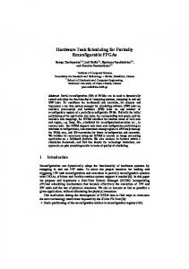
The primary advantage of using arrays of cells to perform multiplication is that the DSP algorithm can exploit the benefits of pipelining. Suppose that we superpipeline the structure in Figure 3 so that each cell occupies one pipeline stage. The clock cycle time thus includes the time to evaluate the m-bit MAC function as well as the time to transfer the result to adjacent cells. Figure 4 labels each cell in the improved MAC unit with the clock cycle at which it calculates the intermediate result. We can then insert the appropriate number of pipeline registers into the module, as depicted by slashes in the figure.
A19:16 A15:12 A11:8 A7:4 A3:0 D19:16 D15:12 D11:8 D7:4 D3:0 C19:16 C15:12 C11:8 C7:4 C3:0 x+
x+
x+
x+
x+
B3:0 Y3:0
x+
x+
x+
x+
x+
B7:4 Y7:4
x+
x+
x+
x+
x+
B11:8 Y11:8
x+
x+
x+
x+
x+
B15:12 Y15:12
x+
x+
Y39:36 Y35:32
x+ Y31:38
x+ Y27:24
x+ Y23:20
B19:16 Y19:16
Figure 3. Improved MAC unit (n=20, m=4)
The pipelining scheme in Figure 4 has one disadvantage: the m-bit portions of the B input must be broadcast across several columns of cells during the same clock cycle. Depending on the architecture of the reconfigurable device, such an operation may not be feasible. One way to eliminate the broadcast is to pipeline all the internal lines of the MAC unit. As shown in Figure 5 for the 20-bit case, this change increases the total latency of the module to 3n/m – 2. This additional delay should be negligible for most DSP algorithms, since the multiplier still initiates one operation per clock cycle. For example, to multiply two 20-bit vectors of 1000 elements, the former design requires 1008 cycles, whereas the latter design requires 1012 cycles. If the clock cycle time can be reduced due to the absence of broadcast operations, the MAC unit with pipelined internal lines actually achieves higher performance. A19:16 A15:12 A11:8 A7:4 A3:0 D19:16 D15:12 D11:8 D7:4 D3:0 C19:16 C15:12 C11:8 C7:4 C3:0 5
A19:16 A15:12 A11:8 A7:4 A3:0 D19:16 D15:12 D11:8 D7:4 D3:0 C19:16 C15:12 C11:8 C7:4 C3:0 1
1
1
1
1
2
2
2
2
7
4
3
3
3
6
5
4
4
8
Y39:36 Y35:32
7 Y31:38
6 Y27:24
5 Y23:20
6
5
4
3
B3:0
B15:12
B19:16 Y19:16
B7:4 Y7:4
9
8
7
6
5
B11:8 Y11:8
11
10
9
8
7
B11:8
Y15:12 9
1
B7:4
Y11:8 7
2
B3:0
Y7:4 5
3
Y3:0
Y3:0 3
4
B15:12 Y15:12
13 Y39:36 Y35:32
12
11 Y31:38
10 Y27:24
9 Y23:20
B19:16 Y19:16
Figure 5. Superpipelined MAC unit with pipelined internal lines
3. Two’s-Complement Multiplier
pipeline latches
Figure 4. Superpipelined MAC unit
The latency of this superpipelined design equals the length of the critical path, or 2n/m – 1 cycles. However, the structure can initiate one operation per clock cycle, making the resulting throughput very high. Notice that the MAC unit generates the Y output in a staggered fashion: the least significant m bits in the first cycle, the next m bits in the second cycle, and so forth. The B input should also arrive in this staggered fashion.
As a rule, DSP algorithms work with both positive and negative numbers, so it is reasonable to expect that applications may require two’s-complement multiplication. In fact, the same multiplier structure can be used to perform this operation, except that some cells evaluate slightly different functions. Before we discuss these modifications, recall from (4) that each cell in the unsigned MAC unit evaluates the m-bit MAC function y2m–1:0 = (am–1:0 × bm–1:0) + cm–1:0 + dm–1:0.
(4)
Figure 6 illustrates how these m-bit terms are defined for various cells in the design. For consistency, the c input to the cell always appears to the left of the d input. c3:0
a3:0 d3:0 x+ y7:4
c3:0
a3:0 c3:0
a3:0
b3:0
x+
y7:4 y3:0
b3:0 d3:0
x+
y3:0
y7:4
b3:0 d3:0 y3:0
unsigned portion of B. The cell also adds two’scomplement portions of C and D to the result. In order to represent the entire range of valid outputs, the B cell must generate a 2m-bit output y whose upper m bits and lower m bits are both two’s-complement numbers. This data format is unusual, but is the best choice for representing the result. One can think of the cell as generating two m-bit outputs satisfying the expression
Figure 6. Cells in improved MAC unit
2my2m–1:m + ym–1:0 = (am–1:0 × bm–1:0) + cm–1:0 + dm–1:0.
Now consider a two’s-complement MAC unit that handles n-bit inputs in m-bit portions. From the properties of two’s-complement numbers, the most significant m-bit portion has two’s-complement format, but the remaining m-bit portions have unsigned format. Hence, if we modify the unsigned MAC unit to perform two’s-complement arithmetic, many of the cells will still operate on unsigned inputs. Figure 7 depicts the two’s-complement multiplier for n=20 and m=4. Solid lines denote unsigned data; dashed lines denote two’s-complement data.
where am–1:0, cm–1:0, dm–1:0, y2m–1:m, and ym–1:0 are in two’scomplement format. Table 1 lists several example 4-bit calculations for the B cell. Recall that a 4-bit two’scomplement numbers ranges from –8 to 7, whereas a 4-bit unsigned number ranges from 0 to 15.
A19:16 A15:12 A11:8 A7:4 A3:0 D19:16 D15:12 D11:8 D7:4 D3:0 C19:16 C15:12 C11:8 C7:4 C3:0 B
A
A
A
A
B3:0 Y3:0
D
C
A
A
A
B7:4 Y7:4
D
A
C
A
A
B11:8 Y11:8
D
A
A
C
A
B15:12 Y15:12
H Y39:36 Y35:32
F
F Y31:38
F Y27:24
E Y23:20
B19:16 Y19:16
two’s complement line
Figure 7. Two’s-complement MAC unit (m=20, n=4)
Observe that some of the cells generate two’scomplement outputs, whereas other cells do not. In fact, the two’s-complement MAC unit contains seven types of cells, labeled A through H in the figure (G is missing for technical reasons). The A cells simply evaluate the unsigned MAC function in (4). However, the B cell must multiply the two’s-complement portion of A with an
(6)
Table 1: Example calculations of the B cell a3:0 5 5 –5 –5 7 –8
b3:0 5 10 5 10 15 15
c3:0 5 5 5 –5 7 –8
d3:0 –5 5 –5 –5 7 –8
y7:4 2 4 –2 –4 7 –8
y3:0 –7 –4 7 4 7 –8
y7:0 = 16y7:4 + y3:0 25 60 –25 –60 119 –136
A similar analysis can be performed for the remaining cells used in the multiplier. For example, the C cells generate an unsigned output y2m–1:m and a two’scomplement output ym–1:0. With the data formats shown in Figure 7, the n-bit multiplier can generate a two’scomplement output Y without additional hardware. Table 2 lists the input and output format of each type of cell (including the G cell used later). A “+” sign denotes unsigned format, and a “–” sign denotes two’scomplement format. Table 2: Data format requirements for each cell Type A B C D E F G H
am–1:0 + – + – + + + –
bm–1:0 + + + + – – + –
cm–1:0 + – + – – + – –
dm–1:0 + – – + + – + –
y2m–1:m + – + – – – + –
ym–1:0 + – – + + + – +
4. Hierarchical Multiplier
where
The last two sections have demonstrated that n-bit MAC units in general require seven types of cells. Each cell performs the MAC function on m-bit inputs, but different cells use different data formats. A natural question is how each cell can implement the required mbit operations. For m=1, a simple combinational circuit suffices, but for larger m, the most practical solution may involve some kind of arithmetic unit. For reconfigurable devices, consider the following alternative: to implement the m-bit operations required by each cell, use an m×m array of 1-bit cells. In other words, the proposed architecture contains a two-level hierarchy of cells and “elements”, where cells work with m-bit words and elements work with single bits. The next question is how the m×m array of elements can implement all the functionality required by m-bit cells. For type A cells, the solution is simple: use the unsigned multiplier structure presented in Section 2. As shown in Figure 8 for m=4, each of the elements works with data in unsigned form. Hence, one can classify the elements as type A as well. c3
a3 d3 c 2
a2 d2 c 1
A
A
a1 d1 c 0 A
a0 d0 b0
A
A
A
A
A
b2
A
y2 A
A
y7 y6
A y5
b3
A y4
y3
Figure 8. Type A cell (m=4)
Each element computes the 1-bit MAC function ψ1:0 = (α ∧ β) + γ + δ,
(7)
where α, β, γ, and δ denote the inputs to the element, and ψ signifies the 2-bit output. Note that multiplication reduces to the logical AND operation, denoted by ∧, in the 1-bit case. Each bit of the output ψ can be expressed in terms of the combinational logic functions ψ1 = MAJ(α ∧ β, γ, δ) ψ0 = XOR(α ∧ β, γ, δ),
a3 d3 c 2 B
a2 d2 c 1 A
a1 d1 c 0 A
a0 d0 b0
A
y0 D
C
A
b1
A
y1 D
A
C
b2
A
y2 A
A y5
b3
C y4
y3
Figure 9. Type B cell (m=4)
y1 A
c3
y7 y6
b1
A
(9)
As discussed in the last section, two’s-complement MAC units require additional types of cells. Type B cells, for example, assume that a, c, and d have two’scomplement format, and that b has unsigned format. Using an m×m array of elements to implement a type B cell produces the result in Figure 9.
D
y0 A
MAJ(P, Q, R) = (P ∧ Q) ∨ (P ∧ R) ∨ (Q ∧ R) XOR(P, Q, R) = P ⊕ Q ⊕ R.
(8)
Knowing the data format for each input to the cell, one can determine the format of every internal line using the information in Table 2. The procedure closely parallels the analysis for the two’s-complement multiplier in Figure 7, except that the signal names are Greek symbols instead of lowercase letters. The implementation of the type B cell requires elements of types A, B, and C. Note that both the upper and lower portions of the y output have two’s-complement format, as shown in Figure 7. Continuing on, cells of types C and D have straightforward implementations (Figures 10-11). Type E cells require five types of elements, including type G (Figure 12). Type F cells are similar (Figure 13). Finally, type H cells have the same formatting assignments as the two’s-complement multiplier (Figure 14). This property holds because all the inputs and outputs of a type H cell have two’s-complement format.
c3
a3 d3 c 2 C
a2 d2 c 1 A
a1 d1 c 0 A
a0 d0
c3 b0
A
a3 d3 c 2 C
a2 d2 c 1 A
a1 d1 c 0 A
a0 d0
y0 A
C
A
y0
b1
A
A
C
A
A
C
y1
b2
A
A
A
C
A
y7 y6
A y5
y4
a3 d3 c 2 D
a2 d2 c 1 A
F
F
y7 y6
y3
Figure 10. Type C cell (m=4)
c3
y2
b3
C
F y5
y4
y3
Figure 13. Type F cell (m=4)
a1 d1 c 0 A
A
a0 d0
c3 b0
A
a3 d3 c 2 B
a2 d2 c 1 A
a1 d1 c 0 A
a0 d0
A
b1
A
A
A
b2
A
y0 D
C
A
D
A
y7 y6
A y5
A y4
y1 D
A
C
Figure 11. Type D cell (m=4)
c3
a3 d3 c 2 G
a2 d2 c 1 A
a1 d1 c 0 A
C
a0 d0 b0
A
A
b1
A
y1 A
A
C
b2
A
y2 F y7
F y6
F y5
Figure 12. Type E cell (m=4)
H
F
F y5
b3
E y4
y3
Figure 14. Type H cell (m=4)
y0 A
b2
A
y2
y7 y6
y3
b1
A
y2 b3
b0
A
y1 D
b3
E
y0 D
b2
A
y2 A
b1
A
y1 A
b0
A
–2ψ1 – ψ0 = (–α × β) – γ – δ,
(10)
which simplifies to 2ψ1 + ψ0 = (α ∧ β) + γ + δ.
(11)
b3
E y4
Now consider the MAC function computed by type B elements. From Table 2, the α, γ, δ, ψ1, and ψ0 signals of type B elements all have two’s-complement format. For each of these signals, logic 0 denotes 0 and logic 1 denotes –1. Hence, type B elements compute the expression
y3
Since (11) and (7) are equivalent, elements of types A and B implement the same combinational logic expressions. Performing a similar analysis on the remaining types of cells reveals that only four distinct types of elements are required. In fact, each element implements the same
expression for ψ0; the only difference is the expression used to compute ψ1. Table 3 lists the functions corresponding to each type of element. (Note that ¬ denotes the logical complement.) A reconfigurable architecture could exploit these similarities to implement all necessary operations efficiently. Table 3: Reduction of element types Type A B C D E F G H
ψ1 MAJ(α ∧ β, γ, δ) MAJ(α ∧ β, γ, δ) MAJ(α ∧ β, γ, ¬δ) MAJ(α ∧ β, γ, ¬δ) MAJ(α ∧ β, γ, ¬δ) MAJ(α ∧ β, ¬γ, δ) MAJ(α ∧ β, ¬γ, δ) ¬MAJ(α ∧ β, ¬γ, ¬δ)
ψ0 XOR(α ∧ β, γ, δ) XOR(α ∧ β, γ, δ) XOR(α ∧ β, γ, δ) XOR(α ∧ β, γ, δ) XOR(α ∧ β, γ, δ) XOR(α ∧ β, γ, δ) XOR(α ∧ β, γ, δ) XOR(α ∧ β, γ, δ)
Same as A A C C C F F H
5. Concluding Remarks In this paper, we have presented a novel scheme for performing n-bit multiply-accumulate (MAC) operations using a reconfigurable array of m-bit cells. Each cell computes an m-bit MAC function with two additive terms. The structure can be superpipelined into m-bit units for extremely high throughput, as required in signal processing applications. With suitable changes to the configuration of each cell, the structure can handle unsigned or two’s-complement inputs. To implement the functionality required by each cell, we propose to use an m×m matrix of reconfigurable 1-bit elements. Only four types of elements are required to construct multipliers of any size. As a final note, we have used the concepts presented in this paper to create a two-level reconfigurable architecture for digital signal processing applications [9]. The architecture contains an array of reconfigurable 4-bit cells, each of which consists of a 4×4 matrix of elements. Each element, in turn, uses a 4-input, 2-bit lookup table to evaluate arithmetic or logic functions. Cells can connect to neighboring cells in any direction. However, the matrix of elements can only assume two structures, one of which is the structure of the MAC unit. Having the capability to compute the MAC operation means that cells can perform the arithmetic functions necessary for digital signal processing.
6. Acknowledgment M. Myjak is supported by the U.S. Department of Homeland Security Graduate Fellowship.
7. References [1] R. Tessier and W. Burleson, “Reconfigurable computing for digital signal processing: a survey”, in Y. Hu (ed.), Programmable digital signal processors, Marcel Dekker Inc., 2001. [2] K. Compton and S. Hauck, “Reconfigurable computing: a survey of systems and software,” ACM Computing Surveys, vol. 34, no. 2, Jun 2002, pp. 171-210. [3] K. Rajagopalan and P. Sutton, “A flexible multiplication unit for an FPGA logic block,” in Proc. 2001 IEEE International Symposium on Circuits and Systems, 2001, pp. 546-549. [4] S. Haynes and P. Cheung, “Configurable multiplier blocks for embedding in FPGAs,” Electronics Letters, vol. 34, iss. 7, Apr 1998, pp. 638-639. [5] R. Hartenstein, “Coarse grain reconfigurable architectures,” in Proc. 6th Asia South Pacific Design Automation Conference, Yokohama, Japan, 2001, pp. 564-570. [6] J. Smit et al, “Low cost and fast turnaround: reconfigurable graph-based execution units,” in Proc. 7th BELSIGN Workshop, Enschede, Netherlands, 1998. [7] P. Heysters and G. Smit, “Mapping of DSP algorithms on the MONTIUM architecture,” in Proc. International Parallel and Distributed Processing Symposium, Apr 2003, pp. 180-185. [8] J. Rabaey et al, Digital Integrated Circuits: A Design Perspective, 2nd ed., Upper Saddle River, NJ: Pearson Education, Inc., 2003, pp. 591-592. [9] M. Myjak and J. Delgado-Frias, “A two-level reconfigurable architecture for digital signal processing,” in Proc. 2003 International Conference on VLSI, Las Vegas, NV, Jun 2003, pp. 21-27.