IEEE TRANSACTIONS ON ELECTRON DEVICES, VOL. 56, NO. 5, MAY 2009
1027
Printed Nonvolatile Memory for a Sheet-Type Communication System Tsuyoshi Sekitani, Koichiro Zaitsu, Yoshiaki Noguchi, Kiyoshiro Ishibe, Makoto Takamiya, Member, IEEE, Takayasu Sakurai, Fellow, IEEE, and Takao Someya, Member, IEEE
Abstract—By using state-of-the-art printing technologies and functional inks, we have demonstrated organic nonvolatile flexible random-access-memory matrices with a nondestructive read-out capability and a time-continuous current output; these functionalities have not been simultaneously achieved even by silicon-based conventional memory. A memory cell comprising three transistors becomes possible with inkjet printing and other solution-based processes, which can use ferroelectric copolymer ink comprising poly(vinylidenefluoride-co-trifluoroethylene) and insulating ink comprising polyimide precursors properly within the planer plastic substrate. A large “1 : 0” current ratio of 105 is observed in air when it is annealed at 135 ◦ C, which is sufficiently low to be compatible with many plastic substrates. When stored in air, the “1 : 0” ratio was still 104 after 15 days and 103 after 5 months, which is sufficient for practical applications. Furthermore, human-scale communication sheets were manufactured as the first demonstration utilizing large-area organic memories. Index Terms—Large-area electronics, nonvolatile memory, organic transistors, printing technologies.
I. INTRODUCTION
F
LEXIBLE nonvolatile memories are essential for realizing flexible electronics [1]–[6], including paper-like displays [4], [5] and radio frequency identification tags [6]. Inorganic ferroelectric materials [7]–[9] are used in nonvolatile ferroelectric memories because of their low power consumption and high-speed writing/erasing. However, their high-temperature and/or high-energy fabrication processes preclude the use of plastic film substrates. Recently, organic ferroelectric materials that exhibit large spontaneous polarization have shown promise in discrete devices with ferroelectric capacitance [10]–[14] or ferroelectric transistor structures [15]–[18]. The next step is to fabricate the 2-D array of memory cells; however, full integration of organic memory matrices is prevented by the
Manuscript received June 23, 2008; revised December 23, 2008. First published March 4, 2009; current version published April 22, 2009. This work was supported in part by Core Research for Evolutional Science and Technology, by the Japan Science and Technology Agency, and by Special Coordination Funds for Promoting Technology. The review of this paper was arranged by Editor S. Deleonibus. T. Sekitani, K. Zaitsu, Y. Noguchi, K. Ishibe, and T. Someya are with the Quantum-Phase Electronics Center, School of Engineering, University of Tokyo, Tokyo 113-8656, Japan (e-mail:
[email protected]). M. Takamiya is with VLSI Design and Education Center, University of Tokyo, Tokyo 113-8656, Japan. T. Sakurai is with the Center for Collaborative Research, University of Tokyo, Tokyo 153-8904, Japan. Color versions of one or more of the figures in this paper are available online at http://ieeexplore.ieee.org. Digital Object Identifier 10.1109/TED.2009.2015169
incompatibility of their fabrication processes with those of other electronic components. In this paper, we have demonstrated that organic randomaccess-memory matrices can be realized by using state-ofthe-art materials science and printing technologies. This new type of memory is nonvolatile and mechanical flexible with a nondestructive read-out capability, and maintains a timecontinuous current and/or voltage; these functionalities have not been simultaneously achieved even by silicon-based conventional memory. The ferroelectric copolymer ink used is poly(vinylidenefluoride-co-trifluoroethylene) [P(VDF–TrFE)] with 80 mol.% vinylidenefluoride (VDF), which is the highest reported thus far. A memory cell comprising three transistors becomes possible with inkjet printing and other solution-based processes, which can use ferroelectric ink and insulating ink properly within the planer plastic substrate. This is the first demonstration of integration of multiple functional organic transistors with different gate polymeric dielectric materials on the same film. Furthermore, human-scale communication sheets were manufactured as the first demonstration utilizing large-area organic memories. II. FERROELECTRIC COPOLYMER P(VDF–TrFE) is classified as a fluorinated ferroelectric copolymer. This material exhibits excellent spontaneous polarization, which may be due to the difference in electronegativity between hydrogen and fluorine [13], [14]. In this paper, 80 mol.% of VDF and 20 mol.% of trifluoroethylene (TrFE) are used. A schematic illustration of P(VDF–TrFE) is shown in Fig. 1(a). P(VDF–TrFE) is a crystalline material, and thus, annealing is necessary to enhance its spontaneous polarization. To investigate the annealing effect for P(VDF–TrFE), 400-nm-thick P(VDF–TrFE) films were annealed at different temperatures ranging from 80 ◦ C to 180 ◦ C; these films were sandwiched between Au electrodes to form a capacitance structure. Fig. 1(b) shows the polarization as a function of the applied voltage. P(VDF–TrFE) annealed at 120 ◦ C exhibited very little polarization and no hysteresis. This is quite reasonable because it has been reported that the transition from the paraelectric to ferroelectric state occurs at 100 ◦ C−125 ◦ C [13], [14]. In sharp contrast, after annealing at 135 ◦ C, we observed large polarization and hysteresis. The observed saturation and remnant polarizations were as high as 9.5 and 8.4 μC/cm2 , respectively. However, annealing at above 150 ◦ C degraded the polarization
0018-9383/$25.00 © 2009 IEEE
Authorized licensed use limited to: UNIVERSITY OF TOKYO. Downloaded on May 5, 2009 at 10:56 from IEEE Xplore. Restrictions apply.
1028
IEEE TRANSACTIONS ON ELECTRON DEVICES, VOL. 56, NO. 5, MAY 2009
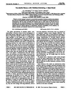
Fig. 1. P(VDF–TrFE). (a) Molecular structure of P(VDF–TrFE); the molar ratio of VDF to TrFE is 8 : 2 in this paper. (b) Polarization of P(VDF–TrFE) annealed at different temperatures. (c) (top) Remnant polarization (PR ) and (bottom) rms values of the surface roughness of P(VDF–TrFE) film as a function of annealing temperature. Large remnant polarization was observed when P(VDF–TrFE) was annealed at 135 ◦ C ± 5 ◦ C in air for 2 h. (d) AFM images. Surfaces of P(VDF–TrFE) films annealed at (top) 135 ◦ C and (bottom) 150 ◦ C. The surface becomes rougher with increasing annealing temperatures above 150 ◦ C since the melting point is approximately 150 ◦ C.
because the melting point of P(VDF–TrFE) is approximately 150 ◦ C. Fig. 1(c) shows the remnant polarization (PR ) as a function of annealing temperature, which clearly indicates that the highest remnant polarization can be obtained after annealing at 135 ◦ C ± 5 ◦ C, which is sufficiently low to be compatible with almost all plastic substrates. The surface of P(VDF–TrFE) became smooth (the rms value of surface roughness was 3.5 nm) on annealing at 135 ◦ C ± 5 ◦ C in air [Fig. 1(c) and (d)]. These results indicate that the ferroelectric characteristics of P(VDF–TrFE) strongly depend on the annealing process; thus, highly crystalline thin films processed under optimized conditions will have enhanced spontaneous polarization and surface smoothness.
III. MANUFACTURING PROCESS Organic nonvolatile memory cells were formed with threetransistor structure; one organic ferroelectric transistor (memory transistor) and two organic transistors (access and erase transistors). All the transistors were manufactured using an inkjet printer (Ricoh Printing Systems Co. Ltd.; IJP-1), a screen printer (Micro-tec Co. Ltd.; MT-550), a microdroplet dispensing system (Musashi-engineering Inc.; Shotmaster 300), and vacuum evaporation (ULVAC Co. Ltd.; Ex-200). The base film (substrate) was of polyimide (Ube Industries Ltd.; UPILEX-75S), with a thickness of 75 μm. Ag nanoparticles (Harima Chemical Co. Ltd.; NPS-J-HP) were patterned by inkjet printing and cured at 180 ◦ C to form 300-nm-thick gate
Fig. 2. Individual organic transistor and ferroelectric transistor. (a) Crosssectional view. Manufacturing process is described in Section III. (b) Printed organic transistors. (c) Transfer characteristic of organic ferroelectric transistor (memory transistor) where the P(VDF–TrFE) gate dielectric layer was annealed at 135 ◦ C. (d) Transfer characteristic of organic transistor with polyimide gate dielectric layers for access and erase transistors.
electrodes and all the word lines. Epoxy partitions were formed around the gate electrodes by using screen printing. Polyimide precursors (Kyocera Chemical Co. Ltd.; KEMITITE CT4112) were diluted using N -methyl-2-pyrrolidone to form insulating polyimide ink with a viscosity of 10 mPa · s. Diluted polyimide precursors were inkjet printed and cured at 180 ◦ C to form 500-nm-thick polyimide gate dielectric layers for the access and erase transistors. Similarly, a ferroelectric copolymer, i.e., P(VDF–TrFE) (Toray-engineering Co. Ltd.; VDF/TrFE molar ratio of 8 : 2), was diluted using N, N -dimethylformamide to form a ferroelectric ink. Diluted P(VDF–TrFE) was patterned using the microdroplet dispensing system and cured at 90 ◦ C (10 min) and successively annealed at 135 ◦ C in air (2 h) to form 400-nm-thick ferroelectric gate dielectric layers for the memory transistors. A 50-nm-thick pentacene layer was deposited using vacuum evaporation with rotation mechanics through printed shadow masks to form a channel layer for all the transistors. Again, Ag nanoparticles were patterned by inkjet printing and cured at 140 ◦ C for 3 h to form the source and drain electrodes and bit lines. The volume of the Ag nanoparticles ink is less than 2 pL. The channel length was 30 μm for all the transistors, while the widths of the access, memory, and erase transistors were 16.5 mm, 45 mm, and 300 μm, respectively. The fabrication process was similar to the method reported in [19]. Finally, a 300-nm-thick layer of poly(2-chloro-p-xylylene), i.e., parylene (Daisankasei Co. Ltd.; diX-SR), was uniformly applied using chemical vapor deposition, and a 150-nm-thick evaporated Au layer was successively applied to form an organic/metallic encapsulation layer. The fabrication process and the effects of the encapsulation layers are reported in [20]. Cross-sectional illustration and pictures of the transistors are shown in Fig. 2(a) and (b).
Authorized licensed use limited to: UNIVERSITY OF TOKYO. Downloaded on May 5, 2009 at 10:56 from IEEE Xplore. Restrictions apply.
SEKITANI et al.: PRINTED NONVOLATILE MEMORY FOR A SHEET-TYPE COMMUNICATION SYSTEM
1029
IV. ELECTRICAL CHARACTERISTICS A. Memory Transistors Fig. 2(c) shows the transfer characteristic of a memory transistor with P(VDF–TrFE) annealed at 135 ◦ C. The channel current (IDS ) significantly increased from 10−10 to 10−5 A when the gate voltage (VGS ) was varied from +90 to −90 V and subsequently remained at 10−5 A as VGS was changed from −90 to +30 V. That is, the memory transistor exhibited excellent bistability at a VGS of 0 V; once a VGS of above −60 V was applied to the gate electrode, the memory transistor exhibited high conductivity because of large remnant polarization. In sharp contrast, the memory transistor exhibited very low conductivity at a VGS of above +60 V because pentacene is a p-type organic semiconductor. The current ratio at a VGS of 0 V exceeded 105 even in air, which is suitable for memory elements. All the measurements were performed in air unless otherwise indicated. B. Printed Organic Transistors The access and erase transistors exhibited high mobility of typically 0.6 cm2 /V · s and an ON/OFF ratio in excess of 107 , indicating excellent transistor characteristics, although inkjetprinted source and drain electrodes are directly formed on the pentacene layer. Transfer characteristics of access and erase transistors are shown in Fig. 2(d).
Fig. 3. Organic nonvolatile ferroelectric memory cell with a three-transistor structure. (a) Memory cell comprising an access transistor (ATr), a memory transistor (MTr), and an erase transistor (ETr). The ATr, MTr, and ETr are controlled with one BL and three word-lines: WLA for access transistor, WLM for memory transistor, and WLE for erase transistor. (b) Memory cell. (c) Transfer characteristics of the memory cell. The current through the memory cell is referred to as IM . The “1” state is attained after applying voltages of VWLA = VWLE = −40 V, VBL = +40 V, and VWLM = −60 V, while the “0” state is attained after applying voltages of VWLA = VWLE = −40 V, VBL = −40 V, and VWLM = +60 V. A readout is performed by applying VWLA = +60 to −60 V, VWLE = −40 V, and VBL = −10 V, while VWLM = 0 V. The “1 : 0” current ratio exceeds 105 . (d) A “1 : 0” ratio of the memory cell as a function of the annealing temperature of P(VDF–TrFE). All the measurements were performed in air.
C. Nonvolatile Memory Cell We describe an organic nonvolatile memory cell with three organic transistors (3T) (hereinafter, “memory cell”). One memory cell comprises one memory transistor and two organic transistors (access and erase transistors), which are connected in series [Fig. 3(a) and (b)]. The access, memory, and erase transistors were controlled with one bit line (BL) and three word lines: WLA for the access transistor, WLM for the memory transistor, and WLE for the erase transistor. Fig. 3(c) shows the transfer characteristics of a memory cell with P(VDF–TrFE) annealed at 135 ◦ C. The current through the memory cell is referred to as IM in this paper. The “1” state is attained after applying voltages of VWLA = VWLE = −40 V, VBL = +40 V, and VWLM = −60 V (hereinafter, the “writing voltages”), while the “0” state is attained after applying voltages of VWLA = VWLE = −40 V, VBL = −40 V, and VWLM = +60 V (hereinafter, the “erasing voltages”). A readout is performed by applying VWLA = +60 V to −60 V, VWLE = −40 V, and VBL = −10 V, while VWLM = 0 V (hereinafter, the “reading-out voltages”). After applying the writing voltages, the memory cell exhibited high conductivity with IM reaching 10−5 A (“1” state). After applying the erasing voltages, the cell exhibited very low conductivity, with IM reaching only 10−10 A (“0” state). Thus, the memory cell exhibited a large “1 : 0” current ratio of 105 in air [Fig. 3(c)]. The “1 : 0” ratio of the memory cell was found to strongly depend on the annealing temperature of P(VDF–TrFE). The aforementioned “1 : 0” ratio in excess of 105 could be obtained when P(VDF–TrFE) was annealed at 135 ± 5 ◦ C [Fig. 3(d)],
which is consistent with the results of the remnant polarization measurements shown in Fig. 1(b) and (c). The time required for changing state from “0” to “1” was approximately 40 ms, while the time for changing from “1” to “0” was approximately 10 ms [Fig. 4(a)]. Thus, the programming (writing/erasing) time is slower than that of previously reported nonvolatile memories [7]–[18], since the memory cell has parasitic capacitances in the access, memory, and erase transistors. However, the cell is sufficiently fast for programming actuators, as will be discussed later. With a decrease in the thickness of the P(VDF–TrFE) layer, the writing/erasing voltages can be decreased to less than 60 V [Fig. 4(b)].
D. Reliability Test Reliability tests of the memory cell were performed in air. Without an organic/metallic encapsulation layer [20], the “1 : 0” ratio of the memory cell was still 103 after storing in air for 3 h [Fig. 5(a) and (b)]. The memory retention time increased considerably with encapsulation layers: when stored in air, the “1 : 0” ratio was still 104 after 15 days and 103 after 5 months, which is sufficient for practical applications. These results clearly demonstrate the excellent data retention characteristics of the memory cell in air. Furthermore, the memory retained a high ratio of above 103 after 104 programming cycles in air [Fig. 5(c) and (d)]; such stability in air has not been previously achieved with organic memories. In fact, previous
Authorized licensed use limited to: UNIVERSITY OF TOKYO. Downloaded on May 5, 2009 at 10:56 from IEEE Xplore. Restrictions apply.
1030
IEEE TRANSACTIONS ON ELECTRON DEVICES, VOL. 56, NO. 5, MAY 2009
Fig. 4. Programming time and voltage. (a) IM as a function of the pulsewidth of the programming voltage. (b) Programming (writing/erasing) voltage as a function of the thickness of the P(VDF–TrFE) layer. The programming voltage decreases with a decrease in the layer thickness. The pulsewidth of the programming voltage is 100 ms.
works on organic ferroelectric memories have employed vacuum, nitrogen, and argon environments [15]–[18]. V. COMMUNICATION SHEET In order to demonstrate the feasibility of the proposed organic memory cell, we developed a new application of organic electronics: a large-area flexible communication sheet with an area of 25 × 25 cm2 . The communication sheet was formed by integrating an organic ferroelectric random-access-memory (FeRAM) sheet comprising 8 × 9 memory cells, a printed plastic mechanical switch sheet [21], [22], a global wiring sheet, and a coil sheet [Fig. 6(a)]. The periodicity of the cell was 1 in [Fig. 5(a)]. The sheet-type organic FeRAM could store and read-out information (“1” or “0”) at arbitrary cell positions. A circuit diagram, pictures, and a cross-sectional view are shown in Figs. 6 and 7. Combining relatively long-distance wired communication and millimeter-scale wireless communication, the sheet offers a new communication method that enables multiple electronic objects scattered over the sheet to communicate with each other by establishing communication paths easily without cumbersome physical connections. The communication route is dynamically formed using printed plastic mechanical switches and global wirings. In addition, a nonvolatile memory sheet stores the routing information. A. Principle Here, we describe the principle of the communication sheet. Assume that two electronic objects—a transmitter and
Fig. 5. Reliability tests. (a) and (b) Retention characteristics in air. (a) Transfer curves of a memory cell measured after being stored in air for 15 days. (b) Current in the memory cell (IM ) as a function of retention time: when stored in air, the “1 : 0” ratio is still 104 after 15 days and 103 after 5 months. IM values for two samples are shown: A) Memory cell with organic/metallic encapsulation. B) Memory cell without organic/metallic encapsulation. (c) and (d) Fatigue characteristics in air and a nitrogen environment. (c) Transfer curves of memory cells measured after 104 programming cycles of in air. (d) IM as a function of programming cycles. IM values for three samples are shown: A) Memory cell with organic/metallic encapsulation. The measurement was performed in air. B) Memory cell without organic/metallic encapsulation. The measurement was performed in air. C) Memory cell without organic/metallic encapsulation. The measurement was performed in nitrogen environment. The “1 : 0” ratio exceeds 103 if the memory cell has organic/metallic encapsulation. The memory cell can retain a high “1 : 0” ratio of above 103 after 104 programming (writing/erasing) cycles in air.
a receiver—are placed on the sheet. 1) The positions of the objects are detected by the position-sensing sheet that we presented in our previous report [22]. 2) The communication path is stored in the organic nonvolatile memories. 3) A path is dynamically formed using the plastic mechanical switches driven by the organic memories. 4) The transmitter sends the signal wirelessly to the communication coil using electromagnetic induction. The signal is transmitted to the other communication coil through the low-resistive Cu wiring of the global wiring sheet and the mechanical switches and is acquired wirelessly by the receiver coils. If the positions are changed, a new communication path is formed. Therefore, dynamic routing can be realized using mechanical switches as dynamic routers. External control chips coordinate among the position-sensing system, the read/write system for the organic memories, and the voltage supply system. B. Coil and Wiring Sheet The coil array and global wiring sheet are formed by a 15-μm-thick Cu layer laminated on a 50-μm-thick polyimide sheet. Thick Cu films are patterned using a screen-printing system. The line width and spacing of the communication coil are both 100 μm. The inductance and resistance of the coil are 27 μH and 25 Ω, respectively. The line width of a line on the
Authorized licensed use limited to: UNIVERSITY OF TOKYO. Downloaded on May 5, 2009 at 10:56 from IEEE Xplore. Restrictions apply.
SEKITANI et al.: PRINTED NONVOLATILE MEMORY FOR A SHEET-TYPE COMMUNICATION SYSTEM
Fig. 6. Communication sheet. (a) A schematic illustration of communication sheet. (b) Circuit diagram. Each cell on the communication sheet comprises a communication coil, a plastic mechanical switch [21], [22], a global wiring sheet, and an organic nonvolatile FeRAM (comprising 8 × 9 memory cells with access, memory, and erase transistors). The periodicity is 1 in. Row 9 does not contain communication coils because it plays the role of a node for interconnecting the seven columns. The access, memory, and erase transistors were controlled with one BL and three word-lines: WLA for the access transistor, WLM for the memory transistor, and WLE for the erase transistor.
1031
Fig. 7. (a) Manufactured large-area communication sheet comprising communication coil sheet, plastic mechanical switch sheet, global wiring sheet, and organic nonvolatile memory sheet. The size of one sheet is 25 × 25 cm2 , and the periodicity is 1 in. (b) Cross-sectional view of one cell of the communication sheet. A communication sheet comprises a communication coil sheet, a plastic mechanical switch sheet, a global wiring sheet, and an organic nonvolatile FeRAM (comprising memory cells with access, memory, and erase transistors). These sheets are manufactured independently using printing technologies. Then, all the sheets are mechanically and electrically connected using hotmelt adhesive sheets (Hitachi-Kasei Co. Ltd.; ANISOLM) that exhibit high conductivity.
global wiring sheet is 5 mm, and it exhibits a low resistance of less than 1 Ω. C. Printed Switch All the electrodes for the printed plastic mechanical switches are formed by inkjet-printed Ag nanoparticles. The electrodes for signal transmission and those for electrostatic attraction are patterned on a 25-μm-thick polyimide membrane. When voltage biases are applied to the electrodes for electrostatic attraction (control electrode), the electrodes on the top sheet are mechanically connected with those on the bottom sheet due to the electrostatic attraction, thereby leading to a very low “ON” resistance. The manufacturing process of the mechanical switch sheet is shown in details in [21] and [22]. To compliment the organic transistors, which have large “ON” resistance (approximately in kiloohms at best) and large parasitic capacitance (∼100 pF), printed plastic mechanical switches were used. The mechanical switches had a very low
operation voltage of 6.6 V and a very low “ON” resistance of a few ohms. Furthermore, the parasitic capacitance of the mechanical switches was less than 0.2 pF, which is two or three orders of magnitude smaller than that of conventional organic transistors. Such low-capacitance mechanical switches are applicable to switching high-frequency signals. The electrode between the memory and erase transistors was connected to the electrode for electrostatic attraction in the mechanical switch, as shown in Fig. 8(a). When the memory cell is in the “1” state, the electrode for electrostatic attraction receives the voltage of the BL (30 V) without a voltage drop because the memory transistor exhibits high conductivity. This brings the mechanical switch into the “ON” state, which allows a signal to be transmitted from the global wiring sheet to a communication coil. On the other hand, when the memory cell is in the “0” state, the voltage of the BL (30 V) does not reach the switch because the memory transistor exhibits very low
Authorized licensed use limited to: UNIVERSITY OF TOKYO. Downloaded on May 5, 2009 at 10:56 from IEEE Xplore. Restrictions apply.
1032
IEEE TRANSACTIONS ON ELECTRON DEVICES, VOL. 56, NO. 5, MAY 2009
the “1” state in the communication path, demonstrating the excellent signal transmission of the sheet. On the other hand, the received signal was less than 1 mV when the memories were in the “0” state [Fig. 8(d)]. VI. DISCUSSION
Fig. 8. Electrical characteristics of communication sheet. (a) Integration of a memory cell and a mechanical switch. The electrode between the memory and erase transistors is connected to the electrode for electrostatic attraction of the mechanical switch. When memory cell is the “1” state, the voltage of the BL (30 V) reaches the switch because the memory transistor exhibits high conductivity. As a result, the mechanical switch turns on, and a signal can be transmitted from the global wiring sheet to a communication coil. The operational voltages for driving the mechanical switches are given as follows: VBL = 30 V; VWLA = −60 V; and VWLM = VWLE = 0 V. (b) Voltage (VM ) supplied from a memory cell as a function of time. The dashed line represents the operational voltage of the mechanical switch when turning on. When the memory cell is in the “1” state, the VM exceeds 6.6 V, and thus, the mechanical switch is turned on. (c) Transmission loss from sender to receiver as a function of the signal frequency. A large ON/OFF ratio can be obtained up to 3 MHz. (d) Sending signal (VS ; 2 V at 2 MHz) and received signal (VR ). When VS is applied from the “sender” end, significant VR is observed at the “receiver” end when the mechanical switch is on (i.e., memory is in the “1” state). VR is less than 1 mV when the mechanical switch is off (i.e., memory is in the “0” state).
conductivity. In this case, the signal from the global wiring sheet is not transmitted to a communication coil. Indeed, the memory cell can supply time-continuous voltages of above 10 V to the electrode of the mechanical switch when the memory is in the “1” state; however, the supplied voltage is 0 V when the memory is in the “0” state [Fig. 8(b)]. In this experiment, a VBL of 30 V, a VWLA of −60 V, a VWLM , and a VWLE of 0 V are applied. D. Characteristics We performed a signal transmission test: A transmitter and receiver were placed on the edges of a communication sheet. A 2-MHz communication signal was used in this experiment, which was the resonance frequency of the system. Fig. 8(c) shows the transmission loss through the communication sheet as a function of frequency. The ON/OFF ratio of the mechanical switch (“1 : 0” ratio of the memory cell) exceeded 103 in the communication signal. However, signals with frequencies greater than 3 MHz were transmitted although the memory was in the “0” state, which may be due to the parasitic capacitances of the system. When a signal VS (2 V at 2 MHz) was applied from the “sender” end, a signal VR (2 V at 2 MHz) was observed at the “receiver” end when the memories were in
The large remnant polarization achieved in the present organic nonvolatile memory cell is attributed to the fact that the TrFE content in P(VDF–TrFE) is the lowest (20 mol.%) among the copolymers reported previously [11]–[18]. The ratio of VDF and TrFE in P(VDF–TrFE) has a major impact on the electrical and solid-state properties, particularly on the remnant polarization, which increases with the ratio of VDF [13]. The P(VDF–TrFE) used in this work exhibited a large remnant polarization of 8.4 μC/cm2 . Such a very high remnant polarization in the organic copolymer is mainly due to the atomic geometry of hydrogen and fluorine and the molecular structure of VDF and TrFE, as well as the optimized annealing processes to stabilize the ferroelectric state [13]. On the other hand, TrFE is indispensable for stabilizing spontaneous polarization and for dissolving VDF in organic solvents, although TrFE has an asymmetric molecular geometry that results in instability to external influences such as solvents and atmospheric components. P(VDF–TrFE) with a VDF/TrFE molar ratio of 8 : 2 exhibits excellent air stability and solubilization, as well as large spontaneous polarization (Figs. 1 and 3). The stability of P(VDF–TrFE) significantly improves the stability of organic memories in air. Furthermore, a simple organic/metallic encapsulation layer [20] is effective in further improving that stability, thus leading to the data retention of 5 months. Although previous organic ferroelectric transistors (1T) have exhibited “1 : 0” ratios of 101 −105 , all the measurements on previously reported ferroelectric memory devices have been performed in vacuum, argon, or nitrogen environments [15]–[18]; that is, no organic nonvolatile memories with air stability have been reported thus far. In addition to air stability, the 3T memory cells exhibit the following three attractive features that are well suited for programming actuators such as mechanical switches [21], [22] distributed over large areas; all the three features are achieved simultaneously within the constraints of a low-temperature flexible-substrate-compatible low-cost large-area printing fabrication approach. First, with organic ferroelectric memory transistors, data (“1” or “0”) stored in the 3T memory cell can be read out without destroying the data by simply applying the reading-out voltages because the memory transistors can permit the flow of reading-out currents with the holding polarization of ferroelectric P(VDF–TrFE). A nondestructive read-out capability has not been reported for organic memories thus far. In commercial ferroelectric memory cells comprising one ferroelectric capacitance and one transistor (1T1C), however, stored data are gradually destroyed when the data are read out because a 1T1C structure can flow reading-out currents with partial flipping of ferroelectric polarization. Therefore, the 1T1C cell can be operated only with pulsed voltages, although such a simple structure is suitable for increasing density of the cells.
Authorized licensed use limited to: UNIVERSITY OF TOKYO. Downloaded on May 5, 2009 at 10:56 from IEEE Xplore. Restrictions apply.
SEKITANI et al.: PRINTED NONVOLATILE MEMORY FOR A SHEET-TYPE COMMUNICATION SYSTEM
1033
printable memory is required for large-area organic electronics where organic sensors and actuators are widely distributed over a large area to make the surfaces intelligent and enhance the functionalities of the devices. For example, in this paper, we have realized the dynamic routing of communication paths with mechanical switches (plastic actuators) where organic memories program the switches distributed over large area. We believe that a higher density of the memory will be required with miniaturizing the sensor or actuator cells in organic electronics, which is an important next step for our works. In the communication sheet, the communication route is dynamically formed using printed plastic mechanical switches and global wirings. Since the information transmitted over the communication sheet is confined to wireline along the ad hoc routed paths, the system is more secure to tapping than ordinary wireless networks and is also free from issues related with the allocation of radio-frequency bands in an already overcrowded airspace. The low power consumption is also important for a very large number of electronic devices to communicate with each other on this sheet. By combining state-of-the-art silicon technologies [30] with the communication sheet, we achieved communication at 107 pJ/bit, which is the lowest energy consumption among wireless communication techniques. The successful manufacturing of the communication sheet with ultralow-power consumption is due to the combination of relatively long-distance wired communication and millimeter-scale wireless communication.
Fig. 9. False writing and erasing. For example, consider achieving the “required state”. If a 2 × 2 memory matrix comprising four ferroelectric transistors with a 1T structure is used, as a first step, we apply voltages of +40, −60, −60, and +40 V to BL0, BL1, WL0, and WL1, respectively, to change the state of the top-left cell from “0” to “1.” Next, −60, +40, +40, and −60 V are applied to BL0, BL1, WL0, and WL1, respectively, to change the state of the bottom-right cell from “0” to “1.” However, simultaneously, the “1” state of the top-left cell is changed to “0.” This is called false erasing. However, if a 2 × 2 memory matrix comprising four memory cells with a 3T structure is used, the “1” state of the top-left cell is not changed because the access transistor is in the OFF state.
Second, the 3T memory cell can maintain a time-continuous current and/or voltage. Importantly, time-continuous voltages can be supplied from the memory cell without a decrease in the voltage, since the memory cell exhibits high conductivity when it is in the “1” state. Furthermore, the direct current bias stress effect [23] is negligibly small in our organic transistors [24]. Third, the 3T memory cell has a significantly reduced probability of false writing/erasing because of the presence of the access transistor (Fig. 9). When a FeRAM matrix is formed using ferroelectric memories with the one transistor (1T) structure, which can supply time-continuous voltages and has the capability for nondestructive readout, false writing/erasing can occur in some specific cases (Fig. 9). In addition to ferroelectric materials, organic nonvolatile memories with simple capacitor structure have been reported [25]–[29], which are, however, functional in vacuum or inert gases or manufactured on glass substrates. The density of memories is always one of the major concerns on Si-based memory storage devices. However, low-density but
ACKNOWLEDGMENT The authors would like to thank Kyocera Chemical Cooperation for providing high-purity polyimide precursors (KEMITITE CT4112), Daisankasei Co., Ltd., for the highpurity parylene (diX-SR), and Toray-engineering Co., Ltd., for the high-purity P(VDF–TrFE). R EFERENCES [1] S. R. Forrest, “The path to ubiquitous and low-cost organic electronic appliances on plastic,” Nature, vol. 428, no. 6986, pp. 911–918, Apr. 2004. [2] A. L. Briseno, S. C. B. Mannsfeld, M. M. Ling, S. H. Liu, R. J. Tseng, C. Reese, M. E. Roberts, Y. Yang, F. Wudl, and Z. N. Bao, “Patterning organic single-crystal transistor arrays,” Nature, vol. 444, no. 7121, pp. 913–917, Dec. 2006. [3] T. W. Kelley, P. F. Baude, C. Gerlach, D. E. Ender, D. Muyres, M. A. Haase, D. E. Vogel, and S. D. Theiss, “Recent progress in organic electronics: Materials, devices, and processes,” Chem. Mater., vol. 16, no. 23, pp. 4413–4422, Nov. 2004. [4] G. H. Gelinck, H. E. A. Huitema, E. Van Veenendaal, E. Cantatore, L. Schrijnemakers, J. B. P. H. Van der Putten, T. C. T. Geuns, M. Beenhakkers, J. B. Giesbers, B. H. Huisman, E. J. Meijer, E. M. Benito, F. J. Touwslager, A. W. Marsman, B. J. E. Van Rens, and D. M. De Leeuw, “Flexible active-matrix displays and shift registers based on solution-processed organic transistors,” Nat. Mater., vol. 3, no. 2, pp. 106–110, Feb. 2004. [5] J. A. Rogers, Z. Bao, K. Baldwin, A. Dodabalapur, B. Crone, V. R. Raju, V. Kuck, H. Katz, K. Amundson, J. Ewing, and P. Drzaic, “Paper-like electronic displays: Large-area rubber-stamped plastic sheets of electronics and microencapsulated electrophoretic inks,” Proc. Nat. Acad. Sci. USA, vol. 98, no. 9, pp. 4835–4840, Apr. 2001. [6] P. F. Baude, D. A. Ender, M. A. Haase, T. W. Kelley, D. V. Muyres, and S. D. Theiss, “Pentacene-based radio-frequency identification circuitry,” Appl. Phys. Lett., vol. 82, no. 22, pp. 3964–3966, Jun. 2003.
Authorized licensed use limited to: UNIVERSITY OF TOKYO. Downloaded on May 5, 2009 at 10:56 from IEEE Xplore. Restrictions apply.
1034
IEEE TRANSACTIONS ON ELECTRON DEVICES, VOL. 56, NO. 5, MAY 2009
[7] H. Ishiwara, M. Okuyama, and Y. Arimoto, Ferroelectric Random Access Memories—Fundamentals and Applications. Berlin, Germany: Springer-Verlag, 2004. [8] B. H. Park, B. S. Kang, S. D. Bu, T. W. Noh, J. Lee, and W. Jo, “Lanthanum-substituted bismuth titanate for use in non-volatile memories,” Nature, vol. 401, no. 6754, pp. 682–684, Oct. 1999. [9] T. Kojima, T. Sakai, T. Watanabe, H. Funakubo, K. Saito, and M. Osada, “Large remanent polarization of (Bi, Nd)4 Ti3 O12 epitaxial thin films grown by metalorganic chemical vapor deposition,” Appl. Phys. Lett., vol. 80, no. 15, pp. 2746–2748, Apr. 2002. [10] K. Noda, K. Ishida, A. Kubono, T. Horiuchi, H. Yamada, and K. Matsushige, “Remanent polarization of evaporated films of vinylidene fluoride oligomers,” J. Appl. Phys., vol. 93, no. 5, pp. 2866–2870, Mar. 2003. [11] A. V. Sorokin, V. M. Fridkin, and S. Ducharme, “Pyroelectric study of polarization switching in Langmuir–Blodgett films of poly(vinylidene fluoride trifluoroethylene),” J. Appl. Phys., vol. 98, no. 4, p. 044 107, Aug. 2005. [12] S. Fujisaki, H. Ishiwara, and Y. Fujisaki, “Low-voltage operation of ferroelectric poly(vinylidene fluoride-trifluoroethylene) copolymer capacitors and metal–ferroelectric–insulator–semiconductor diodes,” Appl. Phys. Lett., vol. 90, no. 16, p. 162 902, Apr. 2007. [13] T. Furukawa, “Ferroelectric properties of vinylidene fluoride copolymers,” Phase Transit., vol. 18, no. 3/4, pp. 143–211, 1989. [14] L. Ibos, A. Bernes, and C. Lacabanne, “Annealing or storage influence on pyroelectricity of ferroelectric PVDF and P(VDF–TrFE) copolymer,” Ferroelectrics, vol. 320, no. 1, pp. 483–489, Jul. 2005. [15] R. C. G. Naber, C. Tanase, P. W. M. Blom, G. H. Gelinck, A. W. Marsman, F. J. Touwslager, S. Setayesh, and D. M. De Leeuw, “High-performance solution-processed polymer ferroelectric field-effect transistors,” Nat. Mater., vol. 4, no. 3, pp. 243–248, Mar. 2005. [16] R. Schroeder, L. A. Majewski, M. Voigt, and M. Grell, “Memory performance and retention of an all-organic ferroelectric-like memory transistor,” IEEE Electron Device Lett., vol. 26, no. 2, pp. 69–71, Feb. 2005. [17] G. H. Gelinck, A. W. Marsman, F. J. Touwslager, S. Setayesh, D. M. de Leeuw, R. C. G. Naber, and P. W. M. Blom, “All-polymer ferroelectric transistors,” Appl. Phys. Lett., vol. 87, no. 9, p. 092 903, Aug. 2005. [18] K. N. N. Unni, R. de Bettignies, S. Dabos-Seignon, and J. M. Nunzi, “A nonvolatile memory element based on an organic field-effect transistor,” Appl. Phys. Lett., vol. 85, no. 10, pp. 1823–1825, Sep. 2004. [19] Y. Noguchi, T. Sekitani, and T. Someya, “Printed shadow masks for organic transistors,” Appl. Phys. Lett., vol. 91, no. 13, p. 133 502, Sep. 2007. [20] T. Sekitani and T. Someya, “Air-stable operation of organic field-effect transistors on plastic films using organic/metallic hybrid passivation layers,” Jpn. J. Appl. Phys., vol. 46, no. 7A, pp. 4300–4306, Jul. 2007. [21] S. Nakano, T. Sekitani, T. Yokota, and T. Someya, “Low operation voltage of inkjet-printed plastic sheet-type micromechanical switches,” Appl. Phys. Lett., vol. 92, no. 5, p. 053 302, Feb. 2008. [22] T. Sekitani, M. Takamiya, Y. Noguchi, S. Nakano, Y. Kato, T. Sakurai, and T. Someya, “A large-area wireless power-transmission sheet using printed organic transistors and plastic MEMS switches,” Nat. Mater., vol. 6, no. 6, pp. 413–417, Jun. 2007. [23] H. L. Gomes, P. Stallinga, F. Dinelli, M. Murgia, F. Biscarini, D. M. de Leeuw, T. Muck, J. Geurts, L. W. Molenkamp, and V. Wagner, “Bias-induced threshold voltages shifts in thin-film organic transistors,” Appl. Phys. Lett., vol. 84, no. 16, pp. 3184–3186, Apr. 2004. [24] T. Sekitani, S. Iba, Y. Kato, Y. Noguchi, T. Someya, and T. Sakurai, “Suppression of DC bias stress-induced degradation of organic field-effect transistors using postannealing effects,” Appl. Phys. Lett., vol. 87, no. 7, p. 073 505, Aug. 2005. [25] J. Ouyang, C. W. Chu, C. R. Szmanda, L. Ma, and Y. Yang, “Programmable polymer thin film and non-volatile memory device,” Nat. Mater., vol. 3, no. 12, pp. 918–922, Dec. 2004. [26] L. D. Bozano, B. W. Kean, M. Beinhoff, K. R. Carter, P. M. Rice, and J. C. Scott, “Organic materials and thin-film structures for cross-point memory cells based on trapping in metallic nanoparticles,” Adv. Funct. Mater., vol. 15, no. 12, pp. 1933–1939, Dec. 2005. [27] H. T. Lin, Z. Pei, J. R. Chen, G. W. Hwang, J. F. Fan, and Y. J. Chan, “A new nonvolatile bistable polymer-nanoparticle memory device,” IEEE Electron Device Lett., vol. 28, no. 11, pp. 951–953, Nov. 2007. [28] T. B. Singh, N. Marjanovi´c, G. J. Matt, N. S. Sariciftci, R. Schwödiauer, and S. Bauer, “Nonvolatile organic field-effect transistor memory element with a polymeric gate electret,” Appl. Phys. Lett., vol. 85, no. 22, pp. 5409–5411, Nov. 2004.
[29] M. Mushrush, A. Facchetti, M. Lefenfeld, H. E. Katz, and T. J. Marks, “Easily processable phenylene-thiophene-based organic field-effect transistors and solution-fabricated nonvolatile transistor memory elements,” J. Amer. Chem. Soc., vol. 125, no. 31, pp. 9414–9423, Jul. 2003. [30] L. Liu, M. Takamiya, T. Sekitani, Y. Noguchi, S. Nakano, K. Zaitsu, T. Kuroda, T. Someya, and T. Sakurai, “A 107 pJ/b 100 kb/s 0.18 μm capacitive-coupling transceiver for printable communication sheet,” in Proc. Dig. Tech. Papers IEEE Int. Solid State Circuits Conf., Feb. 2008, pp. 612–614.
Tsuyoshi Sekitani was born in Yamaguchi, Japan, in 1977. He received the B.S. degree from Osaka University, Osaka, Japan, and the Ph.D. degree in applied physics from the University of Tokyo, Tokyo, Japan, in 1999 and 2003, respectively. From 1999 to 2003, he was with the Institute for Solid State Physics, University of Tokyo, where he developed measurement techniques in magnetic fields up to 600 T and studied the solid-state physics of condensed matter, particularly in high-T c superconductors. Since 2003, he has been a Research Associate of the Quantum-Phase Electronics Center, School of Engineering, University of Tokyo. His current research interests include organic semiconductors and organic-FET devices. Dr. Sekitani is a member of the Materials Research Society, the Physical Society of Japan, and the Japanese Society of Applied Physics.
Koichiro Zaitsu was born in Oita, Japan, in 1984. He received the B.S. degree in applied physics in 2007 from the University of Tokyo, Tokyo, Japan, where he is currently working toward the M.S. degree in applied physics. His research interests include ferroelectric polymers and the new devices integrated with organic transistors. Mr. Zaitsu is a member of the Japanese Society of Applied Physics.
Yoshiaki Noguchi was born in Kanagawa, Japan, in 1983. He received the M.S. degree in applied physics in 2007 from the University of Tokyo, Tokyo, Japan, where he is currently working toward the Ph.D. degree in applied physics. His research interests include organic transistors, large area electronics, and printed electrical devices. Dr. Noguchi is a Student Member of the Japanese Society of Applied Physics. He is also a member of Japan Society for the Promotion of Science Research Fellowships.
Kiyoshiro Ishibe was born in Okayama in 1986. He received the B.S. degree in applied physics in 2008 from the University of Tokyo, Tokyo, Japan, where he is currently working toward the M.S. degree in applied physics. He is currently involved in a new method of spectroscopy based on scanning tunneling microscopy.
Authorized licensed use limited to: UNIVERSITY OF TOKYO. Downloaded on May 5, 2009 at 10:56 from IEEE Xplore. Restrictions apply.
SEKITANI et al.: PRINTED NONVOLATILE MEMORY FOR A SHEET-TYPE COMMUNICATION SYSTEM
Makoto Takamiya (S’98–M’00) received the B.S., M.S., and Ph.D. degrees in electronic engineering from the University of Tokyo, Tokyo, Japan, in 1995, 1997, and 2000, respectively. In 2000, he joined the NEC Corporation, Japan, where he was engaged in the circuit design of highspeed digital LSIs and where he developed the field of on-chip measurement macros to solve power integrity issues. In 2005, he joined the University of Tokyo, where he is currently an Associate Professor of the VLSI Design and Education Center. His research interests include power and signal integrity issues in LSIs, low-power RF integrated circuits, low-power digital circuits, and large-area electronics with organic transistors.
Takayasu Sakurai (S’77–M’78–SM’01–F’03) received the Ph.D. degree in electrical engineering from the University of Tokyo, Tokyo, Japan, in 1981. In 1981, he joined the Toshiba Corporation, where he designed CMOS DRAM, SRAM, RISC processors, DSPs, and SoC solutions. He has worked extensively on interconnect delay and capacitance modeling such as the Sakurai model and the alpha power-law MOS model. From 1988 to 1990, he was a Visiting Researcher at the University of California, Berkeley, where he conducted research in the field of VLSI CAD. Since 1996, he has been a Professor at the University of Tokyo, working on low-power high-speed VLSI, memory design, interconnects, and wireless systems at the Center for Collaborative Research. He is also a consultant to U.S. startup companies. He is the author of more than 400 published technical papers, including 70 invited papers and several books. He has filed more than 100 patents. Dr. Sakurai served as a Conference Chair of the IEEE/Japanese Society of Applied Physics Symposium on VLSI Circuits and the IEEE International Conference on IC Design and Technology, a Vice Chair of the Association for Computing Machinery (ACM)/IEEE Asia and South Pacific Design Automation Conference (DAC), and a Program Committee Member of the IEEE International Solid-State Circuits Conference, the IEEE Custom Integrated Circuits Conference, the ACM/IEEE DAC, the ACM/IEEE International Conference on Computer-Aided Design, the ACM Field Programmable Gate Arrays Workshop, the ACM/IEEE International Symposium on Low-Power Electronics and Design, the ACM/IEEE International Workshop on Timing Issues, and other international conferences. He was a plenary speaker for the 2003 International Solid-State Circuits Conference. He is an elected AdCom member of the IEEE Solid-State Circuits Society and an IEEE Circuits and Systems Society Distinguished Lecturer.
1035
Takao Someya (M’03) received the Ph.D. degree in electrical engineering from the University of Tokyo, Tokyo, Japan, in 1997. In 1997, he joined the Institute of Industrial Science, University of Tokyo, as a Research Associate, where he was appointed as a Lecturer of the Research Center for Advanced Science and Technology (RCAST) in 1998 and as an Associate Professor in 2002. From 2001 to 2003, he was with the Nanoscale Science and Engineering Center, Columbia University, and with Bell Laboratories, Lucent Technologies, as a Visiting Scholar. Since 2003, he has been an Associate Professor of the Department of Applied Physics, Quantum-Phase Electronics Center, School of Engineering, University of Tokyo. His current research interests include organic transistors, flexible electronics, plastic integrated circuits, large-area sensors, and plastic actuators. Dr. Someya is a member of the IEEE Electron Devices Society, the Materials Research Society, and the Japanese Society of Applied Physics. He serves as a Subcommittee Member of the IEEE International Electron Devices Meeting and a Program Cochair of the Third Organic Microelectronics Workshop.
Authorized licensed use limited to: UNIVERSITY OF TOKYO. Downloaded on May 5, 2009 at 10:56 from IEEE Xplore. Restrictions apply.