Rick Leatherman, Bruce Ableidinger, Neal Stollon. First Silicon Solutions (www.fs2.com). Abstract: Real-time analysis and debug of applications running on ...
Processor and System Bus On Chip Instrumentation Rick Leatherman, Bruce Ableidinger, Neal Stollon First Silicon Solutions (www.fs2.com) Abstract:
Real-time analysis and debug of applications running on embedded processors and buses present a challenging verification problem on modern silicon implementations ranging from FPGA to ASIC System-on-Chip (SoC) platforms. Verification of internal processing operations and software execution data from processor sub-systems cannot be adequately addressed using in-circuit emulators or logic analyzers. Debug of user defined logic in real time presents additional challenges. Consequently, On-Chip Instrumentation (“instrumentation”) is rapidly becoming a preferred method of choice for verification/debug/integration of embedded processor sub-systems and system TM application code. First Silicon Solutions (FS2) is an on-chip instrumentation leader in with its family of OCI instrumentation systems and supporting IP. A key advantage of instrumentation is the real-time debug and tracing of code execution and operational interfaces of embedded processors and buses, that are buried in the silicon and not externally visible to users on a real-time basis. As such, instrumentation approaches provide a powerful general solution to embedded processor and on-chip bus debug. TM
This paper is based on instrumentation concepts and technologies, with emphasis on OCI approaches developed by FS2 address embedded System-on-Chip debug. Strategically instrumentation based tools supplement In-Circuit Emulator (ICE), BDM, and JTAG based debug approaches and provide a number of advantages in larger multiprocessor embedded systems. On-Chip Instrumentation technology features including trace capabilities, and hardware event recognizers as will as methods of trace module integration and source-level debugger integration are discussed. Case studies are given for OCI integration with processor cores and in monitoring on-chip (AMBA) buses. Several examples of instrumentation applications using Function Tracing and Performance Analysis are presented. The paper concludes by discussing Emerging Trends in instrumentation, including Real-Time Data Exchange. Multi Chip debug, and NEXUS standards.
1. Introduction to System On Chip Instrumentation: The need for improved methods of observing embedded processor and System on Chip (SoC) operation has increased at a proportional pace to the explosive growth in SoC designs and new Intellectual property (IP) cores that support them. With an ever-shortening development cycle, and often several generations of products being produced in parallel or rapid succession, the need for standardized embedded tools and capabilities that enable quick analysis and debug of the embedded IP is a critical factor in keeping SoC verification a manageable part of the process. As more processing elements, features and functions are simultaneously being embedded into the silicon, the emerging level of embedded complexity outstrips the capability of standalone Logic analyzer, debugger and emulator based diagnostic tools. While these tools allow the capture of data off the system data bus, they work only as long as every access (read and/or write) occurs over the external data bus. This points to an increasing gap in terms of effectively being able to provide the necessary controllability and, in particular, the visibility of the internal operations of a complex system. Instrumentation provides complementary alternative methods to digital simulation, providing a means of viewing and analyzing embedded signals. Simulation, while a critical factor in verification, is not a total verification solution for embedded SoC. Simulation alone cannot address all the facets and nuances of physical hardware. In addition, it is not realistic to simulate large, multi-processor architectures for the extremely large numbers of cycles required to evaluate the software specific aspects of system operation and real world system performance. While accelerated simulation, co-simulation, and emulation environments provide a stop gap method of improving the simulation capability in observing system performance, these often introduce costs and complexities beyond the resources of many projects. On Chip Instrumentation and debug approaches have evolved as a low cost and efficient alternative of increasing system visibility that focuses on the final hardware rather than its model. On Chip Instrumentation is defined as an embedded block that provides external visibility and access of the “inner workings” of an architecture. When properly implemented it provides a real time “peephole” into the operations of
key internal blocks that can not otherwise be accessed in sufficient granularity on a real time basis. The real time visibility and monitoring of key interfaces and buses are increasingly crucial to understanding the dynamics of the operation of system architectures. As a general rule, debug visibility becomes increasingly problematic for highly integrated chips, which have extensive, on-chip memory and caches, peripherals, and a range of on chip buses. The key control and bus signals of interest in a deeply embedded system are often not externally addressable by the physical pins of the device and therefore inaccessible to traditional instrumentation. This accessibility issue inhibits verifying silicon operation, introducing many hardware and software integration roadblocks, since the design team must address how traditional debug tools can be interfaced to work properly in SoC designs. On-Chip instrumentation represents a radical although evolutionary departure from ICE (in-circuit emulator) probing implementations used in embedded processing systems. In the next section we provide a brief perspective on historical approaches to embedded processing system debug, including ICE schemes and test ports such as using BDM and JTAG to provide a reference point for discussion of instrumentation capabilities
2. Background of System-on-Chip debug Capabilities To discuss On-Chip Instrumentation in the proper context, it is useful to examine more traditional embedded systems debug. The ever-increasing trend in the embedded system development is the evolution of products that incorporate diverse processing resources. Over the last decade the embedded systems market has seen a proliferation of new processor architectures ( 8-bit MCUs, DSPs, RISC, application specific co-processors, etc.) provided as Intellectual Property (IP) and focused on SoC integration. Historically, development of each generation of processor IP is accompanied by supporting debug tools. Many currently available cores provide some form of JTAG interface for run control and debug functions. Rapidly emerging adjuncts to JTAG are supporting trace capabilities, usually in the form of a trace port such as the ARM’s ETM (embedded trace module) and MIPS’ EJTAG + TCB (Trace Control Block) allow the benefits of trace for more productive system debug. These tools to a large extent only address the specifics of the processor IP and do not address or facilitate the system application in which the IP is used. While the processors become increasing deeply embedded, traditional development tools for system debug applications can't provide non-intrusive visibility into the highly integrated embedded processor. Applied to processor in-circuit emulators and their derivatives such as JTAG hardware debugging, the system must be placed in special debug modes or halted before being able to probe processor registers or reading/writing to the embedded memories. In many cases, this interruption of the steady state performance of the system introduces (time) intrusive elements into the system operation that can complicate or invalidate the data or operations being observed. This problem grows proportionally to the ever-increasing frequency and complexity of high-performance embedded processors. More general purpose trace control blocks have been developed by FS2 and others for the on-chip instrumentation to provide a vendor independent means of enabling trace as well as triggering and run control capabilities. System-on-Chip debug, in common with most verification philosophies, seeks to maximize test functionality and ease of verification, while reducing the overall end user cost. There is a constant tradeoff that must be made on resources that are dedicated to system analysis and debug, vs. the system cost of including these features. The value of debug is mainly perceived during the development cycle (be it hardware or software) where operational questions and integration issues for the key processing blocks are unresolved. After the system is “fully debugged”, the hardware investment in debug capabilities become much more application focused. This was traditionally a pin and area consideration in the design process, where device pricing and profitability was directly related to die size, and a philosophy of minimizing the test components that did not directly add to revenue prevailed. These tradeoffs have shifted over recent years by dramatic increases complexity, gate availability and overall speed of system operation and has changed the norm in chip design from a “core and gate limited” to an “pin and IO limited” focus. The debug question has migrated from how many gates can be spent on debug to an ease of use and bandwidth issue of how much of the system resources and IO is needed to debug the system successfully. The integration of deeply embedded memory and embedded buses - along with limited IO for such embedded subsystems available for test purposes limits the visibility of the embedded processors in SoC operation and dataflow. These “deep encapsulations” of key system functions, along with higher internal bus speeds make traditional debug techniques such as emulators so limiting they have forced the evolution to new logic analysis and debug approaches such as on-chip instrumentation
2.1 In-Circuit Emulator (ICE) Debug Given the central importance and relative complexities of processor cores in embedded systems, more focus has been placed on processor debug technologies than with most other test related aspects of an embedded system. Historically, the most commonly used processor debug tool is the in-circuit emulator (ICE). In circuit emulation has a long and generally successful history for standalone processor debug but is more limited in the systems environment. Due to architectural differences in processors, diverse ICE tools have been developed [1] and continue to evolve to suit the needs of different processor. In a systems analysis context however, all present some limitations. In ICE operations, the processor operational interfaces are modified, either via software or hardware to allow extended host control of the processor run environment. When the processors are in ICE mode, they were actually in a non-standard operating state of the processor; with differing opcodes and interface features. The resulting operation of a processor in emulation mode makes the processor appear to be in a dormant state, impacting on the ability to concurrently debug other parts of the embedded system. In addition, to be minimally intrusive, many processor emulation schemes are limited to monitoring the processor bus. Many signals, both at the processor periphery and internal registers, are inaccessible during ICE mode operations.
2.2 JTAG Debug The use of a "debug port” has become a widely used stepping stone between traditional processor emulation and more SoC friendly approaches to debug. Debug ports simplify controllability and visibility by providing a low overhead access to internal signals. Most approaches use JTAG, BDM, or variants as a standardized debug port. Back Ground Debug Mode (BDM) is a –bit-serial synchronous communication protocol developed by Motorola as an ICE variant. BDM halts execution of an opcode fetched from memory and starts the internal MCU microcode to process commands received from a dedicated serial debug interface. BDM is primarily interesting as the first example of a debug port whereby commands can be used to view and modify registers and to access into on-chip and external memory locations. Of much wider use for debug and test control are JTAG based ports. 200+ major electronics manufacturers have adapted the JTAG (Joint Test Action Group) standard IEEE 1149.1 since its release in 1990. Originally conceived as a 4 pin Boundary Scan Architecture (BSA) for board level IO testing, JTAG supports a variety of test instructions with a low overhead and low bandwidth serial data access interface. Many processor vendors have evolved JTAG as a means of accessing embedded state information of the microprocessor for testing and run control. By extending the JTAG instruction set to include higher-level "probe mode." instructions for ICE, the JTAG can be used to enter and leave probe mode and access internal JTAG enabled registers. While in probe mode, the processor ICE can examine and modify the internal and external state of a system’s registers, memory, and I/O space. A rich infrastructure of tools environments and standardized debug schemes have been built on this foundation to provide both JTAG debug of embedded processors and other parts of an embedded system. JTAG has evolved into a robust and leading mechanism for debug control. Due to its serial BSA architecture, JTAG is limited in the level of debug visibility it can support. Debug of a single processor in isolation may be based on observation of a limited number of internal registers since the processor may be halted frequently to probe and export additional information. The increased signal complexity of SoC devices, with multiple processing resources, internal buses and other supporting IP makes a JTAG halt and probe approach complex and limiting. This increased complexity for SoC debug requires an instrumentation solution with higher data throughput and operations visibility than JTAG was designed to provide.
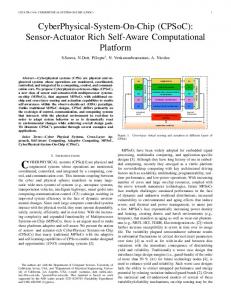
3. On-Chip Instrumentation technology – Overview On Chip Instrumentation was developed as an approach that addresses signal visibility issues of debugging a highly integrated embedded processor and SoC. The need for new debug capabilities has evolved along with the state of embedded processor design. ICE was developed to support debug of processor-based parts with minimal amounts of additional integration, but by emulating operations, rather than executing them normally. The adoption of JTAG popularized the use of a debug port that allows low overhead access and provides embedded developers with a range of potential capabilities for debugging, but with a limited bandwidth never designed to support any real time analysis. Instrumentation adds to the debug port philosophy of JTAG by extending the bandwidth capabilities to address debug of one or multiple cores, internal buses, complex internal peripherals and high speed data traffic
found at SoC levels of complexity. On Chip Instrumentation is, in many ways, a toolkit of resources and analysis philosophies to assist in debug of complex systems rather than a single clearly defined product. Different OCI approaches and implementations are used for debug of, as examples; processors and buses. Optimized instrumentation for different processors can differ significantly, to allow support for architectural differences and features. At its simplest level, instrumentation consists of one or more sets of blocks that allow collection, aggregation, and concentration or compression of selected internal data of an SoC that is desired to trace over time. The signals are exported over device pins for external post processing or visualization. Sophisticated instrumentation blocks support real time data filtering, onchip analysis of target performance and single or multi-core triggering and breakpoint management within the target chip. Widely used features offered by the instrumentation extensions include complex triggers that monitor address, data, and status, branch trace collection, qualified trace collection, task trace and external triggers for cross triggering with other instrumentation, such as logic analyzers for tracing IO level signals. Since the instrumentation blocks must be integrated on chip, typically they are provided as RTL (Register Transfer Logic) hardware Intellectual Property (IP) - i.e. Synthesizable VHDL or Verilog code that can be instantiated in the target design under test. RTL based design allows easier implementation of scalable approaches that support performance vs. resource tradeoffs, allowing debug instrumentation to be integrated over the full lifecycle of a part. Typically more focus on debug features is seen in early (pre-silicon) debug (i.e. hardware emulation or in FPGA devices) with a lesser feature set shipped in final silicon. Traced Internal Signals
Trace collection
Trace concentration
Trace aggregation
Trace Export
Figure 1 - On-Chip Instrumentation blocks perform trace formatting and data export 3.1 Trace and Event Triggering Central to most instrumentation capabilities is the tracing of data as it moves through the application or system. To address differing debug requirements, instrumentation blocks must support different implementations of trace collection. Typical requirements include the ability to trace in cycle, branch and timer modes. Cycle mode collects all bus cycles generated by the core(s). Branch mode collects all execution path changes, sometimes called Branch Trace Messages. Timer trace mode records a frame with a timestamp each time an event is satisfied, providing basic performance analysis measurements. Event recognition is widely used in conjunction with trace to capture information on events and operations in the SoC. Trace data values can be monitored and compared to provide real time triggers to control event actions such as breakpoints and trace collection. Event recognizers can simultaneously look for bus address, data, and control values and be programmed to trigger on specific values or sequences such as address regions and data read or write cycle types. The event recognizers can control enable or disable of breakpoints and trace collection. Data tracing based on recognizable events opens doors to new capabilities in real time SoC analysis. The data trace mode provides real-time information about the status and data of a system’s internal signals, including as examples, analysis of cache performance and internal memory and data transfer operations that can not otherwise effectively be extracted from a system. In line or post processing of trace information allows for analysis of dataflow performance or measurement of systems characteristics such as bus availability or cache hit/misses, which require a long-term steady state (measured over many cycles) system information. Additional detection of events in traced data allows the development environment to flag specific features in the trace data as it flows through the application. ICE techniques that rely on BDM and JTAG implementations cannot provide this data in real-time or with complete visibility of all internal interactions.
As an example of a complex OCI event recognizer feature, four event recognizers can be combined to produce two complex events. In this arrangement, the complex events can be configured so that first event of the event pair must be satisfied before the second event is enabled.
Trace set 1 OCI Signals
Event Recognizer
Trace set 2
Event Recognizer
Trigger
Figure 2 - Example of a complex OCI event recognizer 3.2 External Interfaces for On-Chip Instrumentation JTAG provides the default interfaces for most basic debug functions to embedded blocks. Supporting JTAG, trace and probe ports provide additional IO bandwidth needed for many on-chip instrumentation approaches. Even with these additional ports, the amount of debug information required can easily exceed the allocated debug interface bandwidth of a SoC. To reduce the information sent over the interface, approaches such as data compression and filtering can be used to increase performance of the debug interface with minimal affect to the overall system cost. Obviously, the most useful approach to reducing the information from the debug port to the host development tool is to limit transmissions to new information and have inferred information derived by the development tools. For example, to accurately track execution instruction. If the target processor does not have a change of flow, then the full address need not be transmitted. Only when a change of flow such as an interrupt or branch occurs, would the system need to send the new beginning address. Also, if the debugging session must be real-time, then some constraints of information being sent is required. For instance, grouping data into relevant sets needed for specific export and analysis allows prioritized use of the debug port during run-time. One of the major limiting factors on the use of instrumentation in SoC and multi-core architectures is the ability to quickly export data as it is generated. While On-Chip Instrumentation can address many of the operations associated with large amounts of on chip debug, for example triggering and performance monitoring. There is however, almost always a need to be able to view the debug signals such as instruction/data trace from a processor, which means data must be exported off chip. The ability to transmit debug signals, most notably trace, is a hard limited function of two parameters; 1. the number of IO pins that can be dedicated to export of debug information at any given time, and 2. the speed at which these signals can transmit the data. This problem of exporting debug data is compounded for multiple core SoC architectures, with internal address, data, and control signals for each core, as well as monitoring inter-core and peripheral bus signals. One basic instrumentation approach is to rely on on-chip memory to buffer between traced data and the export bandwidth available. Buffers of modest size however are easily overloaded given a large amount of trace data that is generated in cases of multiple IP blocks or internal buses. Chip packaging becoming an increasingly dominant factor in SoC system costs. Despite the increasing numbers of IO signals available in leading edge packages, system designers must limit the number of IO signals dedicated to trace and debug. To reduce system cost, most current approaches to increasing the IO bandwidth for debug rely on a combination of increasing the effective number of IO pins available (by multiplexing debug mode information into other system pins) and using higher speed IO to increase the throughput of each pin. Each of these approaches to increase debug throughput has advantages and disadvantages. Increasing the effective pin count by statically multiplexing pins is a well-proven and low risk approach. It does however involve coordination over the entire operation of the SoC, since pins that are dedicated for extended clock cycles to debug operations are unavailable for use in other modes of operation. To support SoC core and internal bus speeds, increasing pin bandwidth is required for instrumentation interfaces of a SoC.
4. Performance analysis using On Chip Instrumentation FS2’s OCI philosophy integrates performance analysis of SoC architectures as part of a debug solution. Performance analysis (PA) is somewhat of an all-encompassing term and refers to many types of measurements that provide information on how a particular core is being utilized, both in context of other parts of the system and with regards to specific algorithms. Integrating OCI to allow processor characterization, software performance, and system performance metrics provides valuable and concise information, which is more simply gathered on chip than off. Lack of useful signal visibility at the IO can make embedded processor performance testing challenging. Direct performance analysis is often limited or obscured by the layers of system buses, peripherals, and limited IO access between an embedded processor and the external test environment. Some common types of testing for SoC system performance analysis that OCI an enable are: • Processor Characterization • Software Performance Analysis • System Performance Characterization
4.1 Processor Characterization For processor characterization, the common method of performance monitoring (PM) is to provide a set of counters and a selectable set of processor and bus events to count. A counter reaching a programmed terminal count can generate an interrupt allowing the processor to read and reset counters and log the information. For an embedded processor, performance monitoring modes and counters need to be set up and read out via the JTAG port so that the measurements do not interfere with processor execution. Also important is the ability to use hardware triggers to start and stop measurements so that event counter results can be recorded at specific points in the program. While a single point-to-point measurement can help in determining performance problems, capturing many occurrences of these event counts, in real time, is very useful. By designing the PM module so that the counter outputs can be written to the internal or external trace module, a trigger can be set up to save the counter values into the trace buffer, reset them, then restart them in one clock. A range of measurements that can be made with performance monitoring OCI both to determine the overall performance of a processor and its operations on critical executing algorithms. • • • • • • • • • • •
overall I or D cache hit/miss ratios cache hit/miss ratios in a specific section of code instructions executed per clock number of executed instructions between two points in the program, and how it varies memory access utilization of on-chip or off-chip memory blocks number of processor stalls versus total number of instructions executed number of clocks during which processor is stalled relative to total clock cycles internal bus utilization; i.e. ratio of bus busy to total clocks number of branches taken relative to total number of branch instructions executed mis-predicted branches relative to number of branches taken number of clock cycles between location A and B in the program (A-B timing)
4.2 Software Performance Analysis The purpose of software performance analysis is to find the areas and reasons that certain code that take up significant amounts of executing time, One simple, inexpensive method is called hot-spot profiling where the processor’s program counter (PC) is periodically sampled and binned to provide information on where the processor is spending most of its execution time. On-chip instrumentation to support hot spot profiling provides a means of sampling the current PC without perturbing the target execution. A JTAG command samples the PC then shifts the value out of the device for post-processing.
Another OCI-enhanced method of measuring software performance is for the processor to provide instruction type information to the trace block, specifically, when a call or return instruction is executing or an ISR has been entered or exited. The trace hardware stores only the addresses of these subroutine call/return instructions, providing a qualified trace of call-return flow. Add timestamping to the trace and it can be post-processed to report min, max, and average time in each function, exclusive and/or inclusive of nested functions. A third method of software performance, at an RTOS task level, is enabled by OCI trace hardware that can qualify trace on a contiguous set of memory addresses. Most commercial RTOS can enable instrumentation that writes the new active task ID to a predefined memory location whenever a context switch occurs. Tracing the task ID values along with a duration timestamp results in an almost-zero overhead trace of task execution history.
4.3 System Performance Characterization The OCI hardware described above - consisting of qualified storage on a set of memory writes - can provide another dimension of performance measurement. User-defined instrumentation consisting of markers placed into source code can provide measurement points used for system level characterization down to very detailed application performance. Types of measurements can include: •
• • • •
software throughput of the critical system functions; i.e. how much work per unit time is being done by the processor. Examples would include network packets processed per unit time, streaming blocks of data (such as audio or video data) converted and forwarded to another stage of processing, interrupts processed, graphical data converted to pixels, etc. measure loop times in critical algorithms; determine maximum duration, which may be more critical than the average duration ISR (interrupt service routine) min, max, and average execution times placing markers around code that disables then enables interrupts providing measurement of worstcase interrupt latency thread loop times, defined as the time from when the thread is activated by a semaphore synchronization until it is put to sleep waiting for the semaphore again
For multiprocessor SoC designs, one wants to know bus utilization, whether there is contention when attempting to access the shared bus and if so, how much time does each core wait for the bus and specifically, waiting time for each peripheral (including memory) it accesses from the bus. A performance monitor attached to a bus can measure these types of system factors. It can help determine if the priority scheme implemented by an arbiter for bus accesses is the best one for the system design. For debugging and tweaking system software where there is interaction between multiple cores, instrumented code can be inserted in the source code at the important locations in each core. A bus trace tool such as an AMBA AHB trace can be set up to qualify on writes to a block of shared memory (or a dummy slave device can be placed on the bus). Each core has a small set of instrumentation addresses; the resulting address indicates which core is writing its instrumentation markers. The trace then holds a history of all the locations that have executed in all the cores. With timestamping, the duration of various core events can be displayed, illuminating the parallelism of the code running on the different cores and how software synchronization occurs between them.
5. FS2 CLAM System for OCI This section will review specific OCI technology developed by First Silicon Solutions (FS2) as specific examples of the more general instrumentation requirement and features. FS2 provides OCI capabilities that implement synthesizable debug blocks integrated into SoC level solutions, with a focus on embedded processor architectures. FS2 OCI addresses a range of configurable logic analysis approaches, including embedded processor debugging and system validation features such as run control, trace history, complex breakpoints, and memory and register visibility, and along with embedded bus and signal trace. As in any instrumentation solution, OCI requires support by an external system environment to allow the capture and interpretation of the recorded data. First Silicon Solutions’ Configurable Logic Analysis Module (CLAM) system is representative of the overall environment required to support OCI. The CLAM debug environment consists of the
OCI logic, an analyzer probe, and PC based analyzer software. The probe provides data capture and conversion to and from the OCI, both through JTAG and controlled impedance trace IO (a Mictor connector which provides commonality with other logic analyzer tools). Logic in the probe also performs preprocessing before handoff to the PC tools. The host PC controls the collection process and provides captured history to the user with a choice of graphical or command line interfaces. A controller box interfaces to the target via a JTAG or Mictor connector and manages communications between the OCI debug block and the PC host resident software development tools. The analyzer includes both GUI and command line interfaces (CLI). Having a CLI allows script based operation and post-analysis. The CLAM CLI is based on Tcl/tk, a widely used command language [2]. Command Line Window – Tcl/tk based
Windows MDI/ABI converter
MDI
Windows MDI/ABI DLL - Trace Display, Trigger Control
Probe - Intermediate storage and control - Trace Control - Counters - Event Trigger - Timestamps
Trace Port
Source- level debugger
PC based tool interface and GUI software
Probe interfaces between OCI and Host system
JTAG/EJTAG
OCI for System under test
Synthesizable block integrated to target silicon
Figure 3 – CLAM OCI Debug Environment The OCI includes extensive trigger logic, allowing for both dynamic interactions with the target system and improved capture of information of interest. FS2 analyzers nominally support 4 triggers with up to 4 states per trigger. Trigger conditions can be created as application specific combinations of three components: - raw or processed data (filtered or aligned) compared to logic or edge events on each signal, - counter or times values matching a preprogrammed value, - Trigger state (what trigger related operations have occurred previously) When a trigger condition is satisfied, one or more actions can be taken, such as mark the trigger frame, turn trace on/off, record a single trace frame, turn the counter on/off, increment or clear counter, assert the external trigger out, or change trigger state. The flexibility of this system significantly improves the an engineer’s ability to monitor and tune system performance based on a wide range of operational parameters
5.1 Third Party tool integration - source-level debuggers A wide variety of software tools from multiple vendors may be used in various phases of the SoC design. On-Chip Instrumentation debug environments should interface to tools that are required by the processor type in the design, along with specific RTOS, tool chains, and host development platforms they require. Despite progress in tool plug and play capabilities, integration of multi tool environments can be challenging. To simplify tool integration, FS2 supports an environment with common and well-defined interfaces. CLAM supports the widely adopted MDI interface to provide a debugger environment that allows for a vendor independent integration of both graphical and command line interfaces by supporting a number of vendor neutral formats.
Debugger control software is integrated with a documented Application Binary Interface (ABI) C interface. This is a Windows DLL allowing tools such as source-level debuggers for various processors to interface to the debugger ABI using a well-defined process. FS2 JTAG debugger control hardware allows integration to a variety of GUI and tools front end environments that support ABI based communications.. The FS2 Command Line Interface (CLI) is based on Tcl/Tk, a command language widely used in validation and manufacturing test. FS2 has developed and integrated a number of command primitives and Tcl procedures to customize Tcl for use as a control mechanism for FS2 tools. As examples - commands are included for system configuration, emulation control, memory access including an assembler and disassembler, register access, trace and trigger access, file download, FLASH programming, and status indication.
6. On Chip Instrumentation examples In this section, we discuss some examples that illustrate some of the OCI features previously discussed. In particular, examples are presented for OCI blocks to support embedded processor Trace Run Control and on chip bus monitoring as types of instrumentation needed to support SoC designs.
6.1 Processor Trace/Triggering Control Processor Trace Control (PTC) OCI is an instrumentation block integrated with a processor core that selects, collects, compresses, and streams real time trace data. It consists of a JTAG based controller and configurable trace processing blocks that allow capture of processor bus trace, execution history, and/or other real-time information from the core. PTC blocks can be configured to allow either on-chip or off-chip trace storage, depending on trace depth requirement. PTC can also be configured to collect profiling data for performance analysis. The PTC OCI is easily modified to interface to a variety of Debug Unit interfaces for specific processor cores, allowing PTC control of start/stop execution, single-step, breakpoints, and register/memory access. The TM specific PTC instance shown interfaces to the Debug Unit interface for the LSI Logic ZSP architecture. Trace Port
Trace Memory
Processor Trace Control (PTC)
JTAG Port Debug Unit (DEU)
. . Processor Core
Figure 4 - Processor PTC OCI Integration
The PTC block allows trace history to be captured in several modes, depending on the available bandwidth and information desired. The block can combine trace messages of various lengths into trace words of fixed width suitable for writing into memory, which are then sent to either on-chip memory or through a trace port to off-chip memory. Because the bandwidth of an external trace port is limited, selective information collection is supported. Typical choices include execution trace, data cycle trace, and profiling trace. The PTC Trace collection may also be enabled and disabled by hardware breakpoint registers set to generate trace actions. The PTC typically includes some FIFO to buffer trace words on their way to memory. Since multiple clock cycles may be required to output one trace word, for nominal FIFO sizes, trace data can overflow. The PTC control logic can request stalls to the processor pipeline so that no trace information is lost or setting a flag in the trace buffer indicating that trace information has been missed. Optionally, the PTC can include internal trace memory that allows deeper trace depths. For either implementation, a number of off-chip trace formats including JTAG(serial) and multiplexed trace words is supported.
stall Execution Execution Trace Data
Profiling
Trace Word Formatter
Trace Port Interface
Data Buffering
Internal Memory Control
Data Trace Profiling Manager Control
Trigger Manager
Control Interface
Trigger s JTAG Interface
To Trace Port IO To On-Chip Trace IO RAM
JTAG IO
Figure 5 - Trace Control Block Architecture 6.2 Altera NiosTM Embedded Processor OCI Interface The Nios embedded processor is a configurable RISC core developed by Altera for use in their FPGA platforms. An OCI solution was developed by FS2 for the Nios Embedded Processor with a range of configurable features, to support the user definition of NIOS resources (size of instruction and data buses, numbers of breakpoints, trace memory configuration etc.) The OCI is configured by Altera’s SOPC builder and is implemented as a user-defined Nios peripheral that interfaces to the core via its system bus (Avalon) interface. Trace Port
NIOS OCI
JTAG Port
Probe Interface block (PIB)
JTAG Controller Trace Memory
Trace/Run Control Module
NIOS Processor Core
Figure 6 – Altera Nios OCI Interface Like the previous example, control of the OCI block is handled by a JTAG interface and can be configured for either on-chip or off-chip trace storage. Since the NIOS processor does not have a distinct debug mode, the OCI logic includes a trap implementation to a NIOS software breakpoint.
6.3 AMBA AHB bus monitoring With increasing core density and interconnection of blocks in modern SoC design, monitoring internal bus operations is key capability to debug the entire SoC. The AMBA High-performance Bus (AHB) is a leading on-chip bus Used by many SoC design architectures to communicate between cores. On Chip Instrumentation applied to the AHB captures bus activity and provides system diagnostics in real time. In this case the OCI connects to the AHB address bus, data buses, and various control signals at the bus multiplexed outputs. In AHB, signals are driven from each master and multiplexed onto a common address/data/control bus by a multiplexer controlled by the arbiter. The multiplexed output is fanned out to all the AHB slaves. Similarly, data from each slave is multiplexed onto the common bus and sent to the SoC masters. The instrumentation interfaces is configured to receive address/control and data buses data driven from the currently granted master and currently addressed slave. The OCI passively collects bus activity and transfers the collected
data through a trace port to the external probe interface via 38-pin Mictor connector.
AHB Master
AHB Rd (Slave) Bus
AHB Slave
AHB Master
AHB Wr (Master) Bus
AHB Slave
AMBA monitor OCI
AHB Slave
Figure 7 - OCI interface into an AMBA bus The FS2 AMBA Bus OCI was developed to monitor a range of single-master and multiple-master systems. Additional SoC signals can be included in the trace, such as interrupt requests, bus or core status, and processor control signals. The additional signals are optionally used to compare and recognize specific on-chip activity outside the AHB bus and transmitted to the probe for triggering purposes. AMBA data can be probed in two modes; 1. Bus Cycle Mode, which captures address/control and data signals exactly as they occur per clock on the bus. 2. Bus Transfer Mode, in which the master transfer and slave response, which occur on different clock cycles are aligned onto the same clock cycle, allows the combination of address-data-control event triggering. To more effectively use the available trace buffer, the trace hardware can be configured to filter out Idle and Busy and not Ready cycles where no active data is being transferred. This allows each trace frame to record the critical AHB signals, along with additional user-selectable signals, and a timestamp to aid in performance analysis.
Figure 8 - AMBA bus monitor GUI The host software for the AMBA monitoring provides a good example of a specialized debug interface to support bus operations. Bus values can be viewed either numerically or symbolically. The symbolic representation increases the visibility and comprehension of complex bus operation
7. Near term directions in On Chip instrumentation On chip instrumentation is continuing to evolve along with other areas on SoC design. A number of emerging concepts including widespread adoption of real time data exchange and increased support for multi-processor systems debug will be addresses in next generation of OCI.
7.1 Real-Time Data Exchange Real-time data exchange is the ability to “exchange commands and data with the application while it executes”. This approach to “dynamic instrumentation”, “dynamic variable adjustments”, and “dynamic data collection” was introduced by Texas Instruments and is becoming more widely utilized. Dynamic Data Collection refers to the ability to capture specific address ranges of data from the SoC target and present them to the user on the host machine. The data can be “pulled” periodically by instrumentation or on-demand by the user using the JTAG and/or trace port. “Pulled” data exchange methods of implementation can include a JTAG command that suspends the processor, reads a range of data values from the target, and passes them to the host via the probe interface. Debug data can also be “pushed” from the target based on instrumented code to output variables or arrays periodically (i.e. timer interrupt) or from executing a specific location in code – e.g. when a variable is updated. “Pushed” data exchange can be implemented based on instructions in the target code, such that a range of data will be copied from memory to the instrumentation trace port. The hardware core and instrumentation block provide an instruction that can write memory to the trace port, or a DMA channel configuration that can do a range transfer from memory to the trace port. If the trace port is not available, a breakpoint can be placed in the code and the run control unit fetches the string buffer via JTAG reads. A third technique makes use of “shadow memory” – an external RAM that holds the same image of values as those in the processor’s main memory (or cache). “Shadow memory” techniques include zero-overhead methods in which the instrumentation is set up with a range of addresses to shadow. When a read or write occurs in the address range, the instrumentation captures the address and data value and sends it out the trace port. The probe is programmed to map these shadow addresses to its trace memory so this information is collected in the probe trace memory. The memory is implemented as a pseudo-dual port memory in which the host can read the data periodically and display the results while all in-range data values are still being updated.
7.2 Multi Processor debug Single core approaches for debug and trace often fall short when used in conjunction with multiple cores or with processors interfacing with complex application specific IP. Increasingly SoCs integrate multiple types of cores such as DSP processors or other complex application specific IP operations for a myriad of functions. These cores may be running asynchronously or with variable or indirect communications with each other, making it difficult to time correlate debug information. Complicating multi-core debug issues further is the fact that IP blocks come from a variety of vendors, and usually have different compile and debug environments or levels of debug features. Tasks such as processor interfacing, inter-processor communications, run-time execution and coordination, and data presentation place a significant overhead on the debug requirements for heterogeneous and multi-core chips. In these architectures, the instrumentation block(s) must be customized to support the specific verification and debug requirements of both the processors on a stand-alone basis and in a multi-processing configuration. Among the basic requirements, instrumentation blocks must be diverse enough to effectively communicate debug data with their respective cores and interface to each other to coordinate all of their activities. Instrumentation solutions for on-chip buses provide a valuable resource for visibility and debug in multi-processor designs. For systems that have multiple processors communicating over a standard bus such as AMBA AHB, access to information such as what processor owns the on chip bus can provide valuable context as to the relative communication and stages of processor execution. With increasingly complex bus architectures being introduced, FS2 anticipates that the future generations of multi-processor debug will rely on more extensive tracing and triggering of bus operations to address inter-processor communication issues in conjunction with more specific point solutions for processor specific analysis.
Looking ahead to more complex systems, instrumentation will need to be able to have sufficient “embedded intelligence” to interpret information passing between cores, determine what is needed to be extracted for debug and perform other task aware debug for on chip RTOS or network protocol analysis. Equally challenging is presenting all the diverse debug information in a coherent, understandable way. As in many areas of complex SoC design, new classes of instrumentation are needed to address diverse debug and analysis requirements of emerging architectures.
8. Summary On-Chip instrumentation is a debug technology that in the long term holds promise in radically altering the methods of SOC verification but in the near term addresses many of today's SoC debug challenges. Integrating instrumentation into design hardware enables On-Chip Debug capabilities by providing not only visibility but control features such as breakpoints for developing and integrating System-on-Chip (SoC) application code. On chip instrumentation and debug are critical resources to aid in both processor functional and performance assessment and in effectively evaluating silicon prototypes and first silicon debug and validation. There are a wide range of approaches taken to embedded processor debug, including some standardization efforts for embedded system debug being addressed by IEEE-ISTO Nexus 5001. This standardization effort aims to write a real-time debug interface specification and to bring it to the IEEE-ISTO as an emerging and open industry standard. Nexus standards are based on a broad range of proven and commonly used debug techniques, however to date, Nexus has not seen widespread adoption Based on FS2 experience in developing OCI blocks for many applications and architectures, there is no “magic bullet” instrumentation approach, but rather a number of commonly required capabilities needed to provide a robust debug solution. On chip instrumentation enables a range of widely used best practices in debugging. . Implementing a instrumented interface on SoC designs offers distinct advantages in efficiently implementing run control, real-time instruction and data trace information, RTOS support, memory subsystem, breakpoints and watch-points, to name just a few. First Silicon has developed an instrumentation implementation that is scalable and configurable to map to a range of instrumentation requirements on the SoC. In order to support user definable general purpose or application specific features, FS2 has developed its OCI solutions to be modular to facilitate rapid integration in a number of architectures. Based on this experience, some important considerations and observations in developing and implementing an On Chip Instrumentation solution forms the conclusion of this paper. Instrumentation hardware should be a synthesizable solution, both to facilitate integration into a range of target platforms and to enable its use in hardware emulators (Quickturn, Axis, etc.). Integrating OCI with hardware emulation provides a synchronized method of loading and debugging code in a pre-silicon environment. Synthesizable instrumentation solutions also allow their integration into high-end FPGA parts. FS2 has found that in many cases programmable devices incorporating OCI through their CLAM system are ideal for pre-silicon verification. One of the most important features of an instrumentation capability is to support collection and streaming of data off-chip to a logic analyzer or other trace post-processing environment. FS2 addresses this in all of its OCI solutions whether a core centric debug block, a configurable analyzer for FPGA development or the AMBA bus analyzer. Support for complex event recognition and triggering is also required to provide a robust level of control and monitoring of operations. Complex address/data triggers coupled with bus trace can be used for a range of operations, from multiprocessor synchronization to debugging device drivers. Having a source-level debug GUI coupled with the instrumentation’s complex triggers can rapidly uncover execution errors and problems like improperly defined variables. By coupling timestamps to trace data, complex triggers can be used to provide a range of performance analysis information. JTAG has a long-standing history in embedded systems debug and remains a strong component in any instrumentation solution. JTAG control between the host PC environment and the JTAG pins on target system allows for a well defined and widely used control interface needed for both hardware and software debug. As an example, JTAG based run control along with executed instruction trace allows stepping through application code and setting hardware and software breakpoints to debug program algorithms at the source level.
The ability to interpret debug information is essential. A documented API allows fast, efficient porting of instrumentation to customer specific GUI’s. Scripting of validation and manufacturing tests is a useful means for efficiently leveraging embedded instrumentation. FS2 has found that host tool environments for an OCI solution benefit from command line interfaces that allow effective script file usage. Tcl/tk based command line interface are a widely used and vendor neutral approach to developing such test scripts. Instrumentation solutions for processors should support complete integration into a source-level debug interface to provide access to disassembly information needed to understand the context of application related problems. FS2 and its customers have found it very useful to have the OCI logic included as part of a self-testable system to assure that the system is operating correctly, prior to any other debug activities. Instrumentation extensions can be customized in a range of areas for the system to debug application specific IP. Its value in providing otherwise unavailable visibility into a range of internal systems characteristics including code coverage, RTOS task analysis, protocol analysis, etc. will only increase with larger, more complex, and increasingly deeply embedded next generation architectures.
References [1] “In-Circuit Emulation A powerful hardware tool for software debugging” By Robert R. Collins [2] More information about Tcl can be found at the URL http://www.scriptics.com. Practical Programming in Tcl and Tk by Brent Welch is one of many excellent texts on the subject. [3]”Embedded Systems Design – An Introduction to Processes, Tools, & Techniques”, Berger, Arnold, S., CMP Books.
Authors: Rick Leatherman is President & CEO of First Silicon Solutions (FS2). He has over 20 years experience in development tools, and has championed the concept of On-chip Instrumentation (OCI®) beginning in late 1998. Rick has an EE from Virginia Tech and an MBA from the Tuck School at Dartmouth College. He has written numerous articles on development tools and currently is listed as "co-inventor" on a number of pending patents. Dr. Neal Stollon is a consulting engineer to FS2. He has over 20 years of digital design and processor development experience at Texas Instruments, LSI Logic, Alcatel, and others. Dr. Stollon has a Ph.D. in EE from Southern Methodist University, is a Professional Engineer, has written over 25 papers and holds 7 patents. Bruce Ableidinger is Director of Business Development at First Silicon Solutions (FS2). He has worked in the instrumentation and development tools business for over 25 years including time at Intel and Tektronix. He has a MSCS from Oregon State University and a BSEE from Washington State University. He is co-inventor of 3 patents.