Programmable Neuromorphic Circuits for Spike-based Neural Dynamics Mostafa Rahimi Azghadi∗† , Saber Moradi† , and Giacomo Indiveri† ∗ School
of Electrical and Electronic Engineering, The University of Adelaide, Australia. Email:
[email protected] † Institute of Neuroinformatics, University of Zurich and ETH Zurich, Zurich, Switzerland. Email: [mostafa|saber|giacomo]@ini.phys.ethz.ch
Abstract—Hardware implementations of spiking neural networks offer promising solutions for a wide set of tasks, ranging from autonomous robotics to brain machine interfaces. We propose a set of programmable hybrid analog/digital neuromorphic circuits than can be used to build compact low-power neural processing systems. In particular, we present both CMOS and hybrid memristor/CMOS synaptic circuits that have programmable synaptic weights and exhibit biologically plausible response properties. For the CMOS circuits, we present experimental results demonstrating that they operate correctly over a wide range input frequencies; for the hybrid memristor/CMOS circuits we present circuit simulation results validating their expected response properties.
I. I NTRODUCTION Artificial spike-based neural networks offer a promising paradigm for a new generation of brain-inspired computational models. A wide range of theoretical and computational models have already been proposed for both basic neuroscience research [1], [2] and practical applications [3], [4]. Neuromorphic Very Large Scale Integration (VLSI) circuits represent an ideal technology for implementing these types of networks using hybrid analog/digital design techniques, and for building devices that have a very high potential in a wide range of applications [5]. In particular, the main advantage of implementing these spiking neural networks in neuromorphic VLSI technology is their compactness and low power consumption which are critical features when implementing a large scale neural architectures [6]. Synapses are an essential component of spiking neural networks. They represent at the same time the site of memory (as they store the network’s synaptic weight values), and play a fundamental role in computation (as they implement crucial temporal and non-linear dynamics). In these networks the synaptic weight is directly associated with the activity of pre-synaptic and post-synaptic neurons [1]. Different types of learning algorithms have been proposed, to update the synaptic weight depending on pre- and post-synaptic activity [7]–[9]. The different learning strategies have a profound effect on the post-synaptic neuron functionality and on the spiking-neural network behavior [10]. Implementing such types of synapses and learning mechanisms in compact electronic systems is crucial, for developing efficient large-scale spiking neural networks and brain-inspired computing technologies.
978-1-4799-0620-8/13/$31.00 ©2013 IEEE
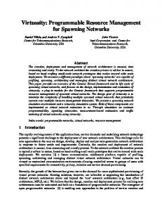
In this paper we present a set of programmable neuromorphic synapse circuits that have been fabricated using standard Complementary Metal Oxide Semiconductor (CMOS) VLSI process [11] and that can support different weight-update mechanisms and learning strategies. Furthermore we propose novel hybrid synapse circuits that apply the same principles used in the programmable CMOS synapses with nano-scale memristive devices [12]–[15]. Specifically, we present a set of experimental results measured from the fabricated synapse circuits demonstrating how they can be calibrated to a specific targeted behavior, and show simulation results for hybrid memristor/CMOS devices demonstrating how they would produce results analogous to the ones obtained with conventional CMOS technology. The paper is organized as follows: Section II briefly describes the architecture of the neuromorphic chip that implements the programmable CMOS synapse circuits. The experimental results measured from the chip synapse circuits, are shown in Section III. Section IV shows the simulated response properties of the hybrid CMOS/memristor synapse circuit. Finally section V is the concluding remarks of this paper. II. A SPIKING MULTI - NEURON CMOS DEVICE The photo micro-graph of the chip comprising the programmable CMOS synapse circuits is illustrated in Fig. 1a. The chip implements a spiking neural network of 32 adaptive exponential Integrate-and-Fire (I&F) neuron circuits [16] with dynamic synapse circuits. All analog circuits on the chip have programmable bias parameters that can be set with an on-chip 32-bit temperature-compensated programmable bias generator [17]. In addition there are 32×32 5-bit digital Static Random Access Memory (SRAM) cells with asynchronous interfacing circuits for storing the weight values of the neural network synapses. The weights can be altered by offchip algorithms that implement different types of synaptic plasticity rules, such as Spike-Timing Dependent Plasticity (STDP) [18]–[20]. The updated weights can be then written back on-chip, to the synaptic weight SRAM memory cells, to change the post-synaptic neuron behavior, for solving cognitive tasks like pattern recognition and classification. The on-chip synapse circuits integrate incoming spikes and produce Excitatory Post Synaptic Currents (EPSCs) with
700
Vdd
Vτs
Vdd 600
Csyn
Iτ
Vdd
Vthrs
Isyn
Bias Generator
SRAM 1024 X 5-bit
neural core
arbitration
Iw
500 1.0
400
Vmem (V)
100 um
Vdd
Firing Rate (Hz)
DPI
300
200
Iw3
w4
w3
Iw1
Iw2 w2
w1
Iw0
w0
async. controller
(a)
(b)
Fig. 1: (a) Chip micro-graph. The multi-neuron chip was fabricated using a standard 0.35 µm CMOS technology and occupies an area of 2.1×2.5 mm2 . The programmable synapses are integrated inside the neural core block. (b) Schematic diagram of the programmable synapse circuit. The top part of the diagram represents a DPI circuit which implements the temporal dynamics. The bottom part of the diagram represents the DAC that converts the SRAM 5-bit weight into a corresponding synaptic current.
amplitudes proportional to their corresponding stored weights. The temporal response properties of the circuit exhibit dynamics that are bio-physically realistic and have biologically plausible time constants [21]. The part of the synapse circuit that produces the slow temporal dynamics is the log-domain Differential Pair Integrator (DPI) filter [22], [23], shown in Fig. 1b. By using the DPI in its linear regime it is possible to time-multiplex the contributions from multiple spiking inputs (e.g., via multiple SRAM cells), thus requiring one single integrating element and saving precious silicon real-estate. This time multiplexing scheme, and circuits implemented on the chip of Fig. 1a have been fully characterized in [11], while the description of the DPI synapse dynamics has been presented in [22]. Here we characterize the response properties of the synapse circuits as a function of input spike frequency and of programmable weight values, and evaluate their linear characteristics and dynamic range properties. III. P ROGRAMMABLE CMOS SYNAPSE RESPONSE PROPERTIES
During the experiments carried out in this section we employed one single post-synaptic neuron and one single input synapse. We characterized the response properties of the combined synapse-neuron circuit by sending input spikes to the synapse, and measuring output spikes from the neuron. The synapse circuit integrates input spikes to produce an output current (the synapse EPSC) that has a mean steadystate amplitude which depends on both the input spike train frequency and its synaptic weight. The silicon neuron integrates this current and produces an output spike train with a mean firing rate that is linear with the current [16] (see
0.6 0.4 0.2 0.0 0.00
100
Iw4
0.8
0.02
0.04
0.06
0.08
0.10
Time (sec) 010
20
30
40
50
60
70
80
90
100
Injection Current (nA)
Fig. 2: Silicon neuron response properties. Mean firing rates of all neurons on the chip, as a function of input current. The figure inset shows the membrane potential of a single neuron.
Fig. 2). Analogous to software models of biological neurons and synapses, the hardware neuron and synapse circuits have multiple parameters that control the way they function. In order to optimize the use of the neuron and synapse circuits in various applications like computation, brain machine interface, pattern recognition etc., it is necessary to tune their analog bias parameters to a set of specific values that results in the required features and expected behavior of the neuromorphic chip. In Fig. 3 we show how it is possible to optimize the circuit biases for a specific range of pre-synaptic frequencies, so that the combined synapse-neuron circuits respond linearly to their afferent synaptic inputs, for all possible weight values that can be programmed. Under this condition, the neuron is able to show identical (gain=1) or linearly higher (gain>1) or lower (gain