Radiation Hardened Phase Change Chalcogenide Memory: Progress and Plans J. Maimon Ovonyx, Inc. 8665 Sudley Rd., #263 Manassas, VA 20110
[email protected]
K. Hunt AFRL 3550 Aberdeen Ave. SE, Bldg. 891
Kirtland AFB, NM 87117-5776
[email protected]
Abstract – The chalcogenide material used for phase-change applications in rewritable optical storage (Ge2Sb2Te5) has been integrated with a 0.5µm radiation hardened CMOS process to produce 64kbit memory arrays. On selected arrays electrical testing demonstrated up to 100% memory cell yield, 100ns programming and read speeds, and write currents as low as 1mA/bit. Devices functioned normally from -55°C to 125°C. Write/read endurance has been demonstrated to 1 × 10⁸ before first bit failure. Total ionizing dose (TID) testing to 2Mrad(Si) showed no degradation of chalcogenide memory element. SEE testing showed no latch-up or single event gate rupture (SEGR) to an LETEFF of 123MeV/mg/cm2. Radiation results show no degradation to the hardened CMOS or effects that can be attributed to the phase-change material. Future applications of the technology are discussed. TABLE OF CONTENTS 1. 2. 3. 4. 5. 6.
INTRODUCTION INTEGRATION WITH CMOS CIRCUIT DEMONSTRATION RADIATION TESTING FUTURE PLANS SUMMARY
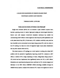
1. INTRODUCTION The term “chalcogen” refers to the Group VI elements of the periodic table. “Chalcogenide” refers to alloys containing at least one of these elements such as the alloy of germanium, antimony, and tellurium discussed here [1-4]. Energy Conversion Devices, Inc., has used this particular alloy to develop a phase-change memory technology used in commercially available re-writeable CD and DVD disks [514]. This phase-change technology uses a thermally activated, rapid, reversible change in the structure of the alloy to store data. Since the binary information is represented by two different phases of the material it is inherently non-volatile, requiring no energy to keep the material in either of its two stable structural states. The two structural states of the chalcogenide alloy, as shown in Fig. 1, are an amorphous state and a polycrystalline state. Relative to the amorphous state, the polycrystalline state shows a dramatic increase in free electron density, similar to a metal. This difference in free
1
J. Rodgers, L. Burcin, K. Knowles BAE SYSTEMS 9300 Wellington Rd Manassas, VA 20110
[email protected]
electron density gives rise to a difference in reflectivity and resistivity. In the case of the re-writeable CD and DVD disk technology, a laser is used to heat the material to change Amorphous State
Polycrystalline State
Figure 1. Transmission Electron Microscope images of the two phases of a GeSbTe alloy.
states. The state of the memory is read by directing a lowpower laser at the material and detecting the difference in reflectivity between the two phases. Ovonyx, Inc., under license from Energy Conversion Devices, Inc., is working with several commercial partners to develop a solid-state non-volatile memory technology using the chalcogenide phase change material [15-18]. To implement a memory the device is incorporated as a two terminal resistor element with standard CMOS processing. Resistive heating is used to change the phase of the chalcogenide material. Depending upon the temperature profile applied, the material is either melted by taking it above the melting temperature (Tm) to form the amorphous state, or crystallized by holding it at a lower temperature
Figure 2. Chalcogenide programming.
(Tx) for a slightly longer period of time, as shown in Fig. 2. The time needed to program either state is ≤ 200ns.
Multiple resistance states between these two extremes have been demonstrated, enabling multi-bit storage per memory cell. However, current development activities are focused on single-bit applications. Once programmed, the memory state of the cell is determined by reading its resistance.
since each memory cell requires an access device (transistor) in addition to the chalcogenide memory element. Such a memory cell, comprised of one access transistor and one chalcogenide resistor, is herein referred to as a 1T1R cell.
Since the data in a chalcogenide memory element is stored as a structural phase rather than an electrical charge or state, it is expected to be impervious to ionizing radiation effects [19]. This inherent radiation tolerance of the chalcogenide material and demonstrated write speeds more than 1000 times faster than commercially available non-volatile memories make it attractive for space-based applications. A radiation hardened semi-conductor technology incorporating chalcogenide-based memory elements will address both critical and enabling space system needs, including standalone memory modules and embedded cores for microprocessors and ASICs.
The ADTC included 272 macros, each with 2 columns of 10 probe pads. Of these, 163 macros were borrowed from existing BAE SYSTEMS’ test structures and used to verify normal transistor operation. There were 109 new macros designed to address the memory element features. These included sheet resistance and contact resistance measurement structures, discrete memory elements of various sizes and configurations, and two 16-bit 1T1R memory arrays.
2. INTEGRATION WITH CMOS Under contract to the Space Vehicles Directorate of the Air Force Research Laboratory (AFRL), BAE SYSTEMS and Ovonyx began the current program in August of 2001 to integrate the chalcogenide-based memory element into a radiation-hardened CMOS process. The initial goal of this effort was to develop the processes necessary to connect the memory element to CMOS transistors and metal wiring, without degrading the operation of either the memory elements or the transistors. It also was desired to maximize the potential memory density of the technology by placing the memory element directly above the transistors and below the first level of metal as shown in a simplified diagram in Fig. 3.
Metal 1
W Stud
Short loop (partial flow) experiments were processed using subsets of the full ADTC mask set. These experiments were used to optimize the process steps used to connect the bottom electrode of the memory element to underlying tungsten studs and to connect an additional tungsten stud level between Metal 1 and the top electrode of the memory element. A full flow experiment was then processed to demonstrate integrated transistors and memory elements.
3. CIRCUIT DEMONSTRATION [20] In order to test the behavior of our chalcogenide cells as circuit elements, we developed the Chalcogenide Technology Characterization Vehicle (CTCV). The CTCV contains a variety of memory arrays with architecture, circuit, and layout variations. Key goals in the design of the CTCV were: 1) to make the read and write circuits robust with respect to potential variations in cell electrical characteristics; 2) to test the effect of the memory cell layout on yield and performance; and 3) to maximize the amount of useful data obtained that could later be used for product design. The CTCV was sub-divided into four chiplets, each containing variations of 1T1R cell memory arrays and various standalone subcircuits. Standalone copies of the array subcircuits were included in each chiplet for process monitoring and read/write current experiments. The arrays all contain 64k 1T1R cells, arranged as 256 rows by 256 columns. This is large enough to make meaningful analyses of parasitic capacitance effects, while still permitting four variations of the array to be placed on each chiplet. The primary differences between arrays consist of the type of sense amp (single-ended or differential) and variations in the location and number of contacts in the memory cell.
Top Electrode Chalcogenide Bottom Electrode Transistor
Figure 3. Chalcogenide memory element integrated with transistor (simplified).
To accomplish this process integration task, it was necessary to design a test chip with appropriate structures. This vehicle was called the Access Device Test Chip (ADTC)
2
The data in the single-ended arrays is formatted as 4096 16bit words (64kbits), and in the differential arrays as 4096 8bit words (32kbits). The 256 columns are divided into 16 groups of 16. One sense amplifier services each group, and the 16 columns in each group are selected one at a time
based on the four most significant address bits. In simulations, stray capacitance was predicted to cause excessive read settling time when more than 16 columns were connected to a sense amp. Each column has its own write current driver, which also performs the column select function for write operations. The single-ended sense amplifier reads the current drawn by a single cell when a voltage is applied to it. The differential amplifier measures the currents in two selected cells that have previously been written with complementary data, and senses the difference in current between them. This cuts the available memory size in half, but increases noise margin and sensitivity. In both the single-ended and differential sense amplifiers, a voltage limiting circuit prevents the chalcogenide element voltage from exceeding VT, so that the cell is not inadvertently re-programmed. On one chiplet, there are two arrays designed without sense amplifiers. Instead, the selected column outputs are routed directly to the 16 I/O pins where the data outputs would normally be connected. This enables direct analog measurements to be made on a selected cell. A third array on this chiplet has both the column select switches and the sense amplifiers deleted. Eight of the 256 columns are brought out to I/O pins. This enables further analog measurements to be made, without an intervening column select transistor.
alone, two-terminal chalcogenide memory elements. These values were used to set the operating points of the write driver circuits and the bias point of the sense amp. A total of forty die of one of the four chiplets, (chip 1) have been packaged for testing, see Figure 4. Chip 1 has four different array configurations, two 64kbit, single ended sense amp arrays and two 32kbit, differential sense amp arrays. Two of the arrays were constructed with the conservative cell layout and two with the aggressive cell layout. Functional test patterns used on these send-ahead devices included all zeros, all ones, checkerboard and checkerboard bar. The results of this testing showed that all circuit functional blocks (control circuits, addressing, data I/O, write 0/1, and sense amp) performed as designed. All four of the array configurations present on the chip showed functional memory elements, i.e., memory cells could be programmed to zero or one and subsequently read out.
Process monitoring structures were included on each chiplet to aid in calibration of memory array test data. These consist of a standalone replica of each of the Write and Read (single-ended) circuits, a CMOS inverter, and a 1T1R cell. The outputs of each of these circuits were brought out to permit measurement of currents versus bias voltages. Pins were provided on the CTCV for external bias voltage inputs to vary the read and write current levels. The standalone copies of the read/write circuits are provided with all key nodes brought out to pins. These replica circuits permit the read and write currents to be programmed by varying the bias voltages. This allows more in-depth characterization to be performed in advance of designing a product. In an actual product, bias voltages would be generated by on-chip reference circuits. Transistor parametric and discrete memory element test structures were tested on the CTCV lot at the wafer level. These tests served two purposes. The first goal was to confirm that the extra processing steps involved in inserting the chalcogenide flow had no effect on the base CMOS technology. No statistical differences in transistor parametric values were noted between these wafers and standard 0.5µm RHCMOS product. The second goal of wafer test was to measure the set, reset and dynamic programming resistances (RSET, RRESET and RDYNAMIC), threshold and holding voltages (VT and VH), and required programming currents (ISET and IRESET) of stand-
3
Figure 4. Wirebond packaged CTCV Chip 1 die.
These devices were also used for determining the optimum bias points of the three externally adjustable parameters: write 0 drive current, write 1 drive current, and the sense amp switching point. An Integrated Measurements Systems XTS-Blazer tester was used to provide stimulus and measure response curves. A wide range of load conditions was chosen based on the measurements performed at wafer test. Using conditions derived from the testing of stand-alone circuit element, the 64kbit arrays were exercised. Array yields were acceptable for characterization and radiation test purposes, with several array variations yielding over 99.9% functional bits. With the addition of the typical redundant rows and/or columns, manufacturability of a 1Mbit or greater device is indicated.
4. RADIATION TESTING [21] Total Ionizing Dose Four CTCV devices were irradiated in a 60Co gamma source. One of the devices was used to characterize the total dose response of the stand alone memory cell, sense amp and write driver circuits while the three other devices were used to evaluate total dose effects on the 64kb memory arrays. The four devices were irradiated to 2Mrad(Si) and measured at intermediate accumulated dose points of 250krad(Si), 500krad(Si) and 1Mrad(Si). The stand-alone circuits were subjected to the electrical characterization testing described above at each readout point. The memory arrays were subjected to functional testing and total device IDD(Q) (four 64kbit arrays in standby) was measured. Resistance of the chalcogenide material was shown to be unaffected by total ionizing dose. In Fig. 5, the R-I curve of an element operated through an NFET access transistor is shown not to have changed after 2Mrad(Si) exposure.
Devices were heated to 125°C during SEL and initial SEU testing. When it was determined that elevated temperature did not affect upset rates, external heating was discontinued. Ion species used were 35Cl (199MeV), 58Ni (265MeV) and 127 I (320MeV). Tilt angles up to 61 degrees were achievable. The maximum effective Linear Energy Transfer (LET) was calculated at 123.2MeV/mg/cm2. Fluences ranging from 3E6 to 5E7 particles/cm2 (adjusted for angle) were achieved using fluxes ranging from 1E4 to 5E5 particles/cm2-second. Calculated penetration depths showed considerable margin beyond the thickness of the memory element, metal layers, and passivation layers on top of the active silicon, even with tilt angles as high as 61 degrees. Direct observation of the parts during testing showed no evidence of shadowing from the socket or other fixtures across the range of tilt angles used. Standard SEL testing performed during dynamic SEE testing showed no latch-up to LETEFF 123MeV/mg/cm2. Two dynamic SEU upset modes were observed. Fig. 6 shows the per-device upset cross-section for transient read upsets. The upsets do not change the contents of the memory cell since subsequent read operations return the originally programmed data. Errors were only observed when reading cells in the high resistance state. The current in the sense amplifier is determined by the resistance of the cell being read, thus the current is much lower when reading a cell with a high resistance and the observed read errors are consistent with transient noise induced in the sense amplifier.
Figure 5. R-I curve for typical discrete memory cell on CTCV. No change was observed to 2Mrad(Si).
Single Event Effects Dynamic SEU and Single Event Latchup (SEL) testing was performed in July 2003 at the Tandem Van de Graaff facility at Brookhaven National Labs on Arrays B and D of three devices. Patterns (checkerboard, all 0’s and all 1’s) were run and monitored continuously in write-read-invertread mode as well as read-only mode. Testing was performed at 3.63VDC. Elevated VDD was chosen because one potential failure mode was a "false write" condition, i.e., the re-programming of a cell due to a single event upset within the write current generator or associated circuitry. High VDD would be worst case for this problem because of the availability of higher current during the proposed false write event.
4
Figure 6. Error cross-section vs. LETEFF curve for transient read disturbs. Note that upsets were only observed during dynamic read of the high resistance memory state.
Fig. 7 shows the per-device cross-section for SEU induced "false writes" during dynamic read-only testing. Errors were only observed when the data in cells with a low resistance were reset to the high resistance state, and only at LETs of 60MeV/mg/cm2 and above. The cell could be reprogrammed post-beam to the correct state, so no Single Event Gate Rupture (SEGR) or other permanent damage mechanisms were observed.
memory goals would be an increase in memory write endurance to >1e14 writes and a reduction in the speed of the device to