Decision-directed carrier recovery decision circuit. +. - exp{-j( )} arg( ) arg( ). W(z). Yk. ^. FF. Xk. ^ filter function. 1. Ë -. - k j e Ï â¦ W(z) exp{-j( )}. FF. Decision.
R. Noé
Real-time Implementation of Digital Coherent Detection R. Noé, U. Rückert, S. Hoffmann, R. Peveling, T. Pfau, M. El-Darawy, A. Al-Bermani
University of Paderborn, Electrical Engineering Optical Communications and High-Frequency Engineering
1
R. Noé
Outline Introduction Real-time constraints for coherent receiver algorithms Angle-based phase estimation for QPSK Combination with polarization multiplex Integrated DSPU for a PDM-QPSK receiver Real-time measurement results Conclusion and outlook
2
R. Noé
Coherent QPSK transmission QPSK transports 2 bits per transmitted optical symbol compared to OOK Lower symbol rate enhances chromatic and polarization mode dispersion tolerance (10 Gbaud Polarization multiplex QPSK ≡ 40 Gbit/s) Feedforward receiver concepts can easily be implemented using digital signal processing compared to classical OPLL approach. Off-the-shelf, low-cost, small-sized DFB lasers suffice in spite of phase noise.
3
R. Noé
4
Coherent optical receiver structure single-chip or modular system TX
90° hybrid ADC Local oscillator LO
ADC 90° hybrid ADC
DSPU Digital Signal Processing Unit
ADC
I1 Q1
I2 Q2
Compensation of intermediate frequency and phase noise, polarization crosstalk, PMD, CD, (nonlinear effects,) … using digital signal processing.
R. Noé
5
Internal structure of the DSPU ADC
ADC
ADC
ADC
1:m demux
1:m demux
1:m demux
1:m demux
T-spaced sampling: fIN = 1/TS T/2-spaced sampling: fIN = 2/TS fDIV = fIN/m
…
…
…
…
feedback path
…
…
…
…
m:1 mux
m:1 mux
m:1 mux
m:1 mux
I1
Q1
I2
Q2
mus Algorith t the r be comp ms eceiv atib le to er st ruct ure!
fOUT = 1/TS
R. Noé
6
Real-time constraints for receiver DSP algorithms
Demultiplexing and parallelization allows to use standard logic elements with relaxed clock speed requirements. Delay robustness of control algorithms for all the cases when feedback loops cannot be avoided at all. Efficient hardware is required to enable a high degree of parallelization with moderate area and power consumption.
R. Noé
Feasibility of parallel processing
ADC
ADC
ADC
ADC
1:m demux
1:m demux
1:m demux
1:m demux
…
…
… …
…
…
…
Demultiplexing to 16…128 parallel channels
…
ADC sampling frequency: 10 GHz to 56 GHz
m:1 mux
m:1 mux
m:1 mux
m:1 mux
I1
Q1
I2
Q2
DSPU clock frequency: 100 MHz to 800 MHz
7
R. Noé
8
Comparison of FIR and IIR filters T α0
T
xk-2
α1
xk
yk
β2
α2 +
+
xk
xk-1
yk serial
yk-2
β1 T
yk-1
T data not instantly available
parallel
+
+
+
+
+
+
+
+
R. Noé
Real-time constraint: Hardware efficiency Computationally complex algorithms increase the required chip area, power consumption and cost. Ways to increase hardware efficiency: • Signal transformations, example: FFT/ IFFT Convolution FFT/IFFT
Multiplication
• Use of look-up tables • Optimization of the required precision
9
R. Noé
10
Real-time constraint: Tolerance against feedback delays
ADC
ADC
ADC
ADC
1:m demux
1:m demux
1:m demux
1:m demux …
…
…
… …
…
…
…
Digital signal processing for coherent optical receivers requires massive • parallel processing, • pipelining.
m:1 mux
m:1 mux
m:1 mux
m:1 mux
I1
Q1
I2
Q2
R. Noé
11
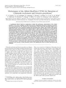
Decision-directed carrier recovery exp{-j( )}
^k ψ
FF
W(z)
Feedback delay of 1 symbol
filter function
e − jψ k −1 ˆ
decision circuit
arg( )
+ ^ Xk
arg( )
e Yk-m+1
… Yk
FF
− jψˆ k −5 m
FF FF FF FF
Decision Decision Decision circuit decision circuit circuit circuit
exp{-j( )}
FF FF FF FF
arg( ) arg( ) arg( )
Linewidth tolerance is significantly reduced!
^ k-4m ψ
FF arg( ) arg( ) FF -+ arg( ) FF arg( ) FF + FF FF FF
FF
+
W(z) + ^ X k-3m+1 …
Yk
X^k-2m
FF
arg( )
FF
R. Noé
Feedforward carrier recovery Viterbi & Viterbi Algorithm [1]: Yk
(·)4
∑
+
2NCR+1
arg(−(·))
ϕˆ k
(·)/4
2. Polarisation 1.5
1
Barycenter-Algorithm [2]: (·)modπ Y arg(·) k
2
ϕk
0.5
ϕˆ k
0
-0.5
2nd Polarization -1
-1.5 -1.5
-1
[1] R. Noé, IEEE J. Lightwave Technology, Vol. 23, No. 2, Feb. 2005, pp. 802-808 [2] S. Hoffmann et al., IEEE Photon. Technol. Lett., Vol. 21, No. 3, Feb. 2009, pp. 137-139
-0.5
0
0.5
1
1.5
12
R. Noé
Barycenter algorithm Im
Inherent weighting due to multiple use of inputs
Re
Yk
arg(·)
(·)modπ2
ϕˆ k
Each filter cell averages pairwise along shortest path.
13
R. Noé
14
Digital synchronous QPSK receiver scheme Differential encoding of data quadrant number nd in TX
Re X
ETX
TX
fiber LO
A/D
l11
ELO l 22
Mod. M
l21 l12
and 1:M DEMUX Im X
Module (i mod M) All signals it needs from neighbor modules are already available.
X(i) (⋅)4
(X(i))4
(X(i−1))4 (X(i−2))4 (X(i−2N))4 Frequency quadrupling
X(i−N)
Mod. 2 Mod. 1
Signal phase ψ(i) arg(⋅)
demultiplexed output data bits o1, o2
Func t iden ionally ti anal cal with og s chem e X ~ ETX ELO*
Quadrant phase number (0, 1, 2, 3) nr(i) no(i)
Differential decoding of Y(i) quadrant LPF (1/4)arg(− (⋅)) phase nj(i) number, ϕ(i) o (i), o2(i) taking carrier Carrier ϕ(i−1) 1 phase jumps phase Lowpass into account angle filtering nr(i−1)
R. Noé
15
Detection and correction of quadrant phase jump ϕ
nj
π/4 nj(i0)⋅π/2
chosen course
0 i0−1
−π/4
i0
i
3
3
2
2
1
1
0
0
nj(i) no(i) = nd(i−N)
3 physical course
nc(i−N)
nr(i)
2 1
nr(i)−nr(i−1)
0
i0−1 Data bits d1, d2 ⇔ quadrant number nd Differential encoding of quadrant number in transmitter: nc (i ) = (nd (i ) + nc (i − 1)) mod 4 Differential decoding of quadrant number in receiver, taking phase jumps into account !
i
i0
d1, Re c, o1
d2, Im c, o2
nd, nc, no
1 -1 -1 1
1 1 -1 -1
0 1 2 3
R. Noé
16
Electronic polarization control X1(i)
R1(i) M R2(i) Z(i)
(X1
(i))4
(X2(i))4
ϕ(i−1)
data recovery 1
Xp(i−N)
nj(i)
data recovery 2
LPF
Y(i)
(⋅)4
ϕ(i)
(1/4)arg(− (⋅))
nr,p(i−1)
Q be a perfect estimate of MJ
−jϕ(l) cos(⋅), sin(⋅) e
X1(l−N), X2(l−N)
op1(i), op2(i)
no,p(i)
nj(i)
(Xp(i))4
M := Q M = (MJ ) M = J −1 −1 = 1− 1− Q Q →1 ⇒ Q ≈1+ 1− Q A be a data vector ⇒ N = (NA )A + −1
ϕ(l)
nr,p(i)
ϕ(i)
Xp(i)
X2(i) Z(i−1) Z(i−2) Z(i−2N)
arg(⋅)
ψp(i)
Q(l) nr,1(l), nr,2(l)
M(l)
−1
−1
( (
))
(
Q(i ) = (1 2)⋅ X(i − N )⋅ e − jϕ (i ) ⋅ r (i )+
M := (1 + g (1 − Q ))M
g ≥ 10 −3 results in well sufficient accuracy
of matrix elements and control time constant on the order of ≤ 103 cycles. At 10 Gbaud control time constants down to ≤ 100 ns are possible.
)
R. Noé
Decision-directed polarization control 1.5
1.5
1
1
0.5
0.5
0
0
-0.5
-0.5
-1
-1
Phase of f are comp sets ensated!
-1.5
-1.5 -1.5
-1
-0.5
0
0.5
1
-1.5
1.5
-1
-0.5
0
0.5
Mk ⎡ Z k ,x ⎤ ⎢Z ⎥ ⎣ k,y ⎦
⎡Y k , x ⎤ ⎢Y ⎥ ⎣ k,y ⎦
1
1.5
Carrier & data recovery
⎡ cˆ k , x ⎤ ⎢ cˆ ⎥ ⎣ k,y ⎦
ϕˆ k
Correlation Matrix-update
M k +1 := M k + g (1 − Q k )M k
Qk
Control target is to force the correlation to the unity matrix. R. Noé, IEEE Photon. Technol. Lett., Vol. 17, No. 4, April 2005, pp. 887-889
Qk
⎡ Y k , x ⎤ − j ϕˆ k =⎢ ⎥e Y ⎢⎣ k , y ⎥⎦
⎡ cˆ k , x ⎤ ⎢ˆ ⎥ ⎢⎣ c k , y ⎥⎦
+
17
R. Noé
18
DSP components for real-time synchronous QPSK transmission Single-chip system
ADC
DEMUX DEMUX
ADC
DSPU
☺ Highest integration → small footprint ☺ Simple interfacing Common technology for ADCs and DSPU → suboptimal performance
ADC ADC
DEMUX
DEMUX
DEMUX
ADC
DEMUX
ADC
DEMUX
ADC
Multi-chip system
DSPU
DEMUX
ADC ☺ Optimum performance ☺ Possibility to use commercial ADCs Complex interface Increased footprint
R. Noé
Chip Specifications SiGe ADC Technology 0.25µm SiGe Resolution 5 bit Number of transistors 3378 Chip size 5.4 mm2 Supply voltage -4 V, 1.8 V Measured power consumption 2.7 W Measured full scale range 410 mV Measured DNL < ± 0.45 LSB Measured INL < ± 0.35 LSB Sampling frequency > 10 GHz Measured input bandwidth > 5GHz
CMOS ASIC Standard Cell Design Gates 306,963 Std. cells 121,576 Max. frequency 625 MHz Supply voltage 1.2 V Power consumption 0.5 W
Full Custom Design Devices 11,838 Max. frequency 10 GHz Supply voltages 1.8 V,1.2V Power consumption 1.5 W
Combined Standard Cell and Full Custom Designs Power 2W Technology 130 nm bulk CMOS Size 15.737 mm2 Pads 146 Supply voltages 1.2 V, 1.8 V
19
R. Noé
5-bit 10-GS/s analog-to-digital converter technology
0.25 μm SiGe:C BiCMOS
resolution
5 bit
number of transistors
3378
chip size
5.4 mm2
supply voltages
-4 V +1.8 V
measured power consumption
2.7 W
measured full scale range (VFSR)
410 mV
measured DNL
< ± 0.45 LSB
measured INL
< ± 0.35 LSB
sampling frequency
> 10 GHz
measured input bandwidth
> 5 GHz (10 GSymbol/s)
measured SNR
up to 30 dB
O. Adamczyk et al., Electron. Lett., Vol. 44, No. 15, July 2008, pp. 895-896
20
R. Noé
Digital signal processing unit
Full-custom
Standard-cell
ASIC
Complexity [transistors]
11,838
1,216,000
1,227,838
Area [mm²]
5.952
5.34
15.737
Frequency [MHz]
5,000 half-rate
625
5,000 half-rate
Power Supply [V]
1.8
1.2
1.8, 1.2
21
R. Noé
Digital signal processing unit
Full-custom
Standard-cell
ASIC
Complexity [transistors]
11,838
1,216,000
1,227,838
Area [mm²]
5.952
5.34
15.737
Frequency [MHz]
5,000 half-rate
625
5,000 half-rate
Power Supply [V]
1.8
1.2
1.8, 1.2
22
R. Noé
23
Components 5-bit 10 Gsample/s flash A/D converter chip Size: 2.1 mm×2.55 mm 0.25µm SiGe
CMOS ASIC 4.1 mm×4.1 mm 130 nm bulk CMOS
Co-packaged module Ceramic substrate 8.5 cm×6.0 cm
R. Noé
10 Gb/s polarization-multiplexed QPSK transmission precoder 4 x 700 Mb/s
PBC DFB laser Signal laser
QPSK modulator
SSMF 80 km
45° PBS
Polarization scrambler
QPSK modulator precoder
I1
5
Q1 I2 Q2
5 DSPU
5 5
ADC
PBS 90° hybrid
ADC PBS ADC ADC
90° hybrid
45°
Local oscillator DFB laser
no x-talk: SOP is manually adjusted, that the polarization cross-talk is minimized. → Switching noise is minimized. x-talk: SOP is manually adjusted, that the polarization cross-talk is maximized. → Switching noise is maximized. 50 rad/s: SOP is scrambled with 50 rad/s on the Poincaré sphere. → Switching noise is the average value of best and worst case.
24
R. Noé
25
Experimental transmission setup precoder 4 x 700 Mb/s
Poincaré sphere traces measured with polarized signal:
PBC
DFB laser Signal laser
QPSK modulator SSMF 80 km
45° PBS QPSK modulator
Photline
precoder
polarization scrambler 12 motorized quarterwave plates HWP
PDL
motorized half-wave plate (bulk optic) I1
PBS 90° hybrid Local oscillator DFB laser
variable PDL element (0…6 dB)
45°
PBS
Q1 I2
90° hybrid
CeLight Israel
Q2
ADC ADC ADC ADC
VOA
5 5 5
Xilinx Virtex 4 FPGA
5 25
R. Noé
Measurement results – fast polarization changes & receiver sensitivity penalty +
c=0.75μs c=3.00 μs 0 krad/s 20 krad/s 40 krad/s
26
R. Noé
Measurement results – polarization-dependent loss
27
R. Noé
28
Generation of fast endless polarization changes by mechanical halfwave plate, inserted between fiberoptic quarterwave plates
R. Noé
Conclusion General real-time requirements for the DSPU: Parallelization Delay tolerance Hardware Efficiency Angle-based phase recovery concept (barycenter): simple, linewidth-tolerant Polarization diversity with automatic polarization demultiplex Realtime coherent receiver implementation: SiGe ADC, CMOS DSPU Test results: 10 Gb/s, 40 krad/s
29
R. Noé
Acknowledgement European Commission FP6 contract 004631 http://ont.upb.de/synQPSK
synQPSK Univ. Paderborn, Germany CeLight Israel Photline, France IPAG, Germany Univ. Duisburg-Essen, Germany
Thank you for your attention!
30