sensors Communication
Real-Time Two-Dimensional Mapping of Relative Local Surface Temperatures with a Thin-Film Sensor Array Gang Li, Zhenhai Wang, Xinyu Mao *, Yinghuang Zhang, Xiaoye Huo, Haixiao Liu and Shengyong Xu * Key Laboratory for the Physics & Chemistry of Nanodevices, and Department of Electronics, Peking University, Beijing 100871, China;
[email protected] (G.L.);
[email protected] (Z.W.);
[email protected] (Y.Z.);
[email protected] (X.H.);
[email protected] (H.L.) * Correspondences:
[email protected] (X.M.);
[email protected] (S.X.); Tel.: +86-10-6276-3276 (X.M.); +86-10-6274-5072 (S.X.) Academic Editor: Vittorio M. N. Passaro Received: 14 March 2016; Accepted: 9 June 2016; Published: 25 June 2016
Abstract: Dynamic mapping of an object’s local temperature distribution may offer valuable information for failure analysis, system control and improvement. In this letter we present a computerized measurement system which is equipped with a hybrid, low-noise mechanical-electrical multiplexer for real-time two-dimensional (2D) mapping of surface temperatures. We demonstrate the performance of the system on a device embedded with 32 pieces of built-in Cr-Pt thin-film thermocouples arranged in a 4 ˆ 8 matrix. The system can display a continuous 2D mapping movie of relative temperatures with a time interval around 1 s. This technique may find applications in a variety of practical devices and systems. Keywords: temperature measurement; multiplexer; real-time; two-dimensional mapping; temperature sensor array
1. Introduction In the past decade, with the rapid development of smart cellphones, wearable and flexible electronics, bioscience and lab-on-a-chip systems, thermal management became a new technological frontier. For novel electronic devices and systems, besides focusing on chip-level thermal management alone, system-level solutions have received much attention. A real-time two dimensional (2D) mapping of the temperature distribution in individual chips and of the whole system could offer unique information for failure analysis, for the improvement of devices and systems, and even for finding optimized dynamic solutions for thermal management [1,2]. For biosciences research, a real-time 2D mapping of temperatures in individual live cells may reveal many unknown phenomena at the single cell and sub-cell levels. For micro- and nano-fluidic systems, real-time 2D mapping of temperature distribution is helpful for a better understanding of local bio-chemical reactions and for better control of the devices. Many techniques have been developed for real-time mapping of surface temperatures, such as infrared imaging, liquid crystal thermography, fluorescence imaging and scanning thermal microscope (SThM), etc. [3–7]. By analyzing the tiny density changes in 80-nanometer-thick aluminum wires using the electron energy loss spectroscopy technique, Mecklenburg et al. recently obtained 2D maps of temperature at the nanoscale in a scanning transmission electron microscope [8]. The temperature data in contactless measurements with infrared or fluorescence imaging are obtained indirectly by calculating shifts in the measured thermal excitation spectra, which usually leads to poor spatial and temporal resolution. The SThM technique measures the temperature by scanning the target surface with a tiny thin film thermocouple or thermal resistance mounted on its probe tip, therefore it Sensors 2016, 16, 977; doi:10.3390/s16070977
www.mdpi.com/journal/sensors
Sensors 2016, 16, 977
2 of 7
has a superior spatial resolution, but the short contact time in the scanning process results in large temperature errors. Due to the requirement for a complicated measurement system, these methods are not applicable for moving objects, or for systems placed under a sealing cover. In these cases, built-in thermal sensors such as resistance temperature detectors (RTD) [9,10], diode sensors [11], and thin-film thermocouples (TFTCs) [12] are better candidates. As passive sensors, TFTCs provide stable performance with a short dynamic response time of 10´9 –10´6 s [13–15], unique flexibility in size, and materials [12,16–19]. In several kinds of TFTCs a moderate thermal power (S) up to 19–26 µV/K and a high temporal resolution of 1–10 mK have been realized [12,17,19]. It was also demonstrated that TFTC arrays could be used to measure high temperatures and give the same readings as commercial K-type thermocouples [20]. A TFTC with a total sensor width of 140 nm, fabricated in a three dimensional (3D) stacking structure, was reported recently, which opens a door towards 2D mapping of local temperatures at the nanoscale with built-in TFTCs [21]. For displaying the 2D distribution of local temperatures T at a chosen time t0 , one needs data T(x,y,t0 ), where (x,y) is the location coordinates. This can be achieved by traceback after obtaining the complete set of time-resolved data [12]. However, to show a real-time 2D mapping of local temperatures, one needs to obtain data T(x,y,t) and display the map quickly. This is challenging, as the number of measurement instruments is usually much less than the number of sensors. A low-noise multiplexer is therefore a proper solution. In this communication, we report a temperature measurement system with one nanovoltmeter, a hybrid electrical-mechanical multiplexer and an array of built-in Cr-Pt TFTCs arranged in an n ˆ m matrix. We performed a dynamic 2D mapping of local temperatures on a sample surface under one or two heating sources. The minimum delay was around 1.0 s, depending on the number of sensors in the array, the rate of temperature change on the sample surface and the pixel density of each frame. 2. Materials and Methods The results reported in this work were obtained with homemade multiplexer circuits, which had an adjustable channel number from 10 to 100. Figure 1a is a photograph of a 32-channel multiplexer. The key elements for these multiplexers were solid relays (G6K-2F-Y-4.5V, Omron, Beijing, China). The “on” or “off” state of each relay was individually controlled with an electronic circuit, and the circuit and nanovoltmeter (2182A, Keithley, Beaverton, OR, USA) were controlled with an automation data acquisition system using the Labview program. This hybrid electrical-mechanical multiplexer reduced system noise to 1–2 µV in fast dynamic measurement process. By averaging ten continuous data points for the same sensor in the same state, the measurement error could be reduced to 0.2–0.5 µV. During measurement, each sensor was individually connected to the nanovoltmeter through a relay. For an array of sensors arranged in an n ˆ m matrix, the nanovoltmeter measured them in sequence from sensor (1,1) to sensor (n,m), then started over again for the next run. The relay had a response time of 3 ms. To ensure a stable and reliable reading for the nanovoltmeter, a delay time of 5–20 ms after sending the triggering signal to each relay could be set in the operation menu, and another waiting time of 20 ms was set before the reading action. Therefore, for a 32-sensor array, the minimum time for each run of measurement was 0.8–1.28 s. For a 10 ˆ 10 matrix, it took 2.5–4.0 s. If averaging of the readings for each sensor was necessary, each run of measurement would take longer. Two display modes could be chosen. In a simple mode, the data for each run of n ˆ m measurements were directly displayed in one frame, and for the locations between the sensor locations the data were calculated with a smooth interpolation algorithm. This is suitable for a slow dynamic process where the temperature varies smoothly and slowly within the total time needed for one run of measurement, 1 s. For a rapid dynamic process, we need to consider the time difference between sensor (1,1) and (n,m), i.e., ~1 s for a 4 ˆ 8 array and ~3 s for a 10 ˆ 10 array. This is just like the correction procedure used for taking digital photographs of a fast moving subject, we need to first fit the curves of temperature versus time for individual sensors, then obtain the temperature distribution at certain time T(x,y,t0 ) and display the 2D map. In this case more than two runs of data were needed
Sensors 2016, 16, 977 Sensors 2016, 16, 977
3 of 7 3 of 7
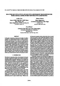
and calculations performed to get T(x,y,t) following a procedure reported previously [12]. weremore needed and morewere calculations were performed to get T(x,y,t) following a procedure reported This leads to a much longer delay time of around 10–30 s, depending on the size of the sensor matrix, previously [12]. This leads to a much longer delay time of around 10–30 s, depending on the size of for firstmatrix, frame of time 2Dof map ofresolved the sample Similarly, the intervalSimilarly, between the the sensor for theresolved first frame time 2Dtemperatures. map of the sample temperatures. two neighboring frames increases frames by several the interval between twoalso neighboring alsofold. increases by several fold. Figure of of thethe whole measurement system in a working state, where sample Figure 1b 1bisisa aphotograph photograph whole measurement system in a working state, the where the with embedded Cr-Pt TFTCs was mounted a green on printed circuit boardcircuit (highlighted), and a heater sample with embedded Cr-Pt TFTCs was on mounted a green printed board (highlighted), (highlighted) was mounted was on top of the sensor distance of The the heater tip of to the the heater sensor tip array, and a heater (highlighted) mounted on toparray. of theThe sensor array. distance to and the motion the heater tip were both controllable X-Y-Z positioner. heating power the sensor array,ofand the motion of the heater tip werewith bothan controllable with anThe X-Y-Z positioner. was at 45power W. In some runs, two with different heating powers wereheating appliedpowers to check the The set heating was set at 45 W.heaters In some runs, two heaters with different were performance of the system. applied to check the performance of the system.
Figure 1. 1. Optical Figure Optical photographs. photographs. (a) (a)The The multiplexer; multiplexer; (b) (b) The The testing testing system system in in aa working working state; state; (c) A sample with 32 Cr-Pt TFTCs arranged in a 4 × 8 matrix (in the yellow square region). Eight TFTC (c) A sample with 32 Cr-Pt TFTCs arranged in a 4 ˆ 8 matrix (in the yellow square region). Eight TFTC sensor junctions junctions in in the the first first row row are are highlighted highlighted with with yellow yellow arrows. arrows. The The inset inset is is an an enlarged enlarged optical optical sensor microscopy image of one TFTC junction region in the second row marked with a red frame, and the microscopy image of one TFTC junction region in the second row marked with a red frame, and the scale bar is 200 μm; (d) An enlarged view of the first row shown in (c). scale bar is 200 µm; (d) An enlarged view of the first row shown in (c).
The Cr-Pt TFTCs were fabricated on 4-inch diameter glass substrates (Jingji Optics, Beijing, The Cr-Pt TFTCs were fabricated on 4-inch diameter glass substrates (Jingji Optics, Beijing, China) China) using standard cleanroom processes including photolithography (MJB4, SUSS MicroTec, using standard cleanroom processes including photolithography (MJB4, SUSS MicroTec, Garching, Garching, Germany), oxygen plasma treatment, magneto-sputtering thin-film deposition (PVD 75, Germany), oxygen plasma treatment, magneto-sputtering thin-film deposition (PVD 75, Kurt J. Lesker, Kurt J. Lesker, Jefferson Hills, PA, USA), and lift-off. The power of magnetron sputtering system was Jefferson Hills, PA, USA), and lift-off. The power of magnetron sputtering system was 120 W with 120 W with base vacuum of 1 × 10⁻⁶ Torr, and pure Ar was used as the operation gas. The bottom Cr ´ 6 base vacuum of 1 ˆ 10 Torr, and pure Ar was used as the operation gas. The bottom Cr layer and layer and top Pt layer were both 100 nm in thickness. The widths of the Cr and Pt stripes were both top Pt layer were both 100 nm in thickness. The widths of the Cr and Pt stripes were both 20 µm. The 20 μm. The nominal thermopower (ΔS*) of the sensor was defined as ΔS* = ΔV/ΔT, where ΔT was the nominal thermopower (∆S*) of the sensor was defined as ∆S* = ∆V/∆T, where ∆T was the calibrated calibrated temperature between the hot and cold ends of each sensor and ΔV was the measured temperature between the hot and cold ends of each sensor and ∆V was the measured output voltage output voltage of the sensor. The calibration method is introduced in the Supplementary Materials. of the sensor. The calibration method is introduced in the Supplementary Materials. 3. Results 3. Resultsand andDiscussion Discussion The circuit circuit noise noise in in continuous continuous dynamic corresponding to to aa The dynamic measurements measurements was was 1.0–2.0 1.0–2.0 μV, µV, corresponding temperature resolution of 0.2 K. Figure 1c shows a sample with an array of 4 × 8 Cr-Pt TFTCs located temperature resolution of 0.2 K. Figure 1c shows a sample with an array of 4 ˆ 8 Cr-Pt TFTCs located in aa 22 ˆ × 22 cm cm22 sensing sensing area area(highlighted (highlightedwith witha ayellow yellowsquare) square) a 4-inch glass substrate. Locations in onon a 4-inch glass substrate. Locations for for the first row of 8 TFTCs were marked with yellow arrows. The 64 contact pads of the 32 sensors the first row of 8 TFTCs were marked with yellow arrows. The 64 contact pads of the 32 sensors were were directly patterned from theCr same Crthin or Pt thinThey films.were Theylocated were located at the fourofedges of the directly patterned from the same or Pt films. at the four edges the sample, sample, each edge consisting 16 pads eight The sensors. is an enlarged optical microscopy each edge consisting 16 pads for eight for sensors. insetThe is aninset enlarged optical microscopy image of image of two sensors in the second row (scale bar 200 μm). Figure 1d is a close view of sensors the five marked sensors two sensors in the second row (scale bar 200 µm). Figure 1d is a close view of the five marked with yellow arrows in the first row as shown in Figure 1c. Seven circular patterns of with yellow arrows in the first row as shown in Figure 1c. Seven circular patterns of Pt thin-film were Pt thin-filmtogether were fabricated together withon thethe Cr-Pt sensors on the sample three with fabricated with the Cr-Pt sensors sample surface, three with asurface, diameter of 2.2 mma diameter of 2.2 mm and four with a diameter of 2.9 mm. These circular pads served as a uniform
Sensors 2016, 16, 977
4 of 7
Sensors 2016, 16, 977
4 of 7
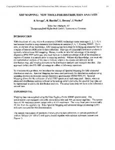
and four with a diameter of 2.9 mm. These circular pads served as a uniform heating zone in the heating experiments. The coldexperiments. ends of TFTCs were on thermally a metal stage to ensureonthe zone in the heating The coldthermally ends of connected TFTCs were connected a temperature the cold kept at room temperature. metal stage toinensure theends temperature in the cold ends kept at room temperature. surface temperatures in The system worked worked well well for forboth bothstatic staticand anddynamic dynamicdistribution distributionofoflocal local surface temperatures the sensing area. Figure 2 shows four typical results in a 3D manner, where the ∆T coordinate shows in the sensing area. Figure 2 shows four typical results in a 3D manner, where the ΔT coordinate the temperature increase as compared to the cold ends, are kept room These shows the temperature increase as compared to the coldwhich ends, which areatkept attemperature. room temperature. four 3D maps are taken from a continuous movie of real-time mapping experiments. In the resting These four 3D maps are taken from a continuous movie of real-time mapping experiments. In the state, when heating is source touching samplethe surface, thesurface, measured values of all resting state,nowhen no source heating is the touching sample thetemperature measured temperature the 32 sensors are32near zero,are as shown in Figure 2a. As 2b, two heaters2b, aretwo putheaters on two values of all the sensors near zero, as shown in shown Figure in 2a.Figure As shown in Figure opposite edges of the sensor area at the same time, and after 20 s, the two edges under the heating are put on two opposite edges of the sensor area at the same time, and after 20 s, the two edges under sources increase their temperatures by 28 K and 26 respectively. heating the heating sources increase their temperatures by K 28atKthe andpeak 26 Kpositions, at the peak positions, After respectively. for 50 heating s, these two peaks show increases of 37 K and 35 K, in Figure Finally, After for 50 s, these two peaks show increases ofrespectively, 37 K and 35asK,shown respectively, as2c. shown in when the two heaters are moved to the center region, it creates one larger heating zone and gradually Figure 2c. Finally, when the two heaters are moved to the center region, it creates one larger heating the peak a temperature increase of 61 K, as shown in of Figure zone andsaturates graduallyatthe peak saturates at a temperature increase 61 K,2d. as shown in Figure 2d.
Figure 2. 2. Measurement Measurement results results taken taken from from a continuous continuous real-time mapping of a sample. (a) The The resting resting state; (b) 20 20 ssafter aftertwo twoheaters heatersare are fixed opposite edges at same the same (c) After 50 s, fixed at at thethe twotwo opposite edges at the time;time; (c) After 50 s, these these two edges increase in temperature; (d)moving After moving two heaters to theofcenter of the two edges increase in temperature; (d) After the twothe heaters both to both the center the sensing sensing region and heating forthe 2 min, the central zone saturates in its temperature distribution. region and heating for 2 min, central heatingheating zone saturates in its temperature distribution.
Note that the relative dynamic temperature distribution in the sensing area is most valuable, Note that the relative dynamic temperature distribution in the sensing area is most valuable, while the absolute temperature values shown in the ΔT coordinate are not accurate. This is because while the absolute temperature values shown in the ∆T coordinate are not accurate. This is because the ΔT value is calculated from the output voltage ΔV by ΔT = ΔV/ΔS*, but ΔS*, the nominal the ∆T value is calculated from the output voltage ∆V by ∆T = ∆V/∆S*, but ∆S*, the nominal thermopower, is changed with the calibration method (see Supplementary Materials). For different thermopower, is changed with the calibration method (see Supplementary Materials). For different systems, people may use different calibration methods to give reliable readings of the measured systems, people may use different calibration methods to give reliable readings of the measured temperatures [12,22,23]. To reveal closely the tip temperature of the heater used in this work, ΔS* is temperatures [12,22,23]. To reveal closely the tip temperature of the heater used in this work, ∆S* is chosen as 10 μV/K. This value was obtained by an on-site calibration procedure that the tip chosen as 10 µV/K. This value was obtained by an on-site calibration procedure that the tip temperature temperature was first determined with a small, standard K-type thermocouple and then the voltage was first determined with a small, standard K-type thermocouple and then the voltage output of each output of each sensor was measured when the tip was put on the junction region, touching it with a sensor was measured when the tip was put on the junction region, touching it with a thin polymer thin polymer buffer layer (see Supplementary Materials). buffer layer (see Supplementary Materials). Figure 3 illustrates the real-time mapping of temperature distribution when a heat source moves from a location outside of the sensing region to the up-left corner, staying there for 80 s, then moved continuously across the sensing area from the top-left corner to the bottom-right corner. Figure 3a–d show the results of the first 80 s process, at t = 20, 40, 60 and 80 s: an increase in temperature by 90 K in the top-left. Figure 3e–p show the results from t = 100 s to t = 320 s, when the
Sensors 2016, 16, 977
5 of 7
Figure 3 illustrates the real-time mapping of temperature distribution when a heat source moves from a location outside of the sensing region to the up-left corner, staying there for 80 s, then moved continuously the sensing area from the top-left corner to the bottom-right corner. Figure 3a–d Sensors 2016, 16, across 977 5 of 7 show the results of the first 80 s process, at t = 20, 40, 60 and 80 s: an increase in temperature by 90 K in the top-left. Figuremoves 3e–p show results from tand = 100 to bottom-right t = 320 s, when the heater moves to heater gradually to thethe central region, to sthe corner, and gradually finally moves away the central region, region. and to the bottom-right corner, finally moves from thesample sensing region.But In from the sensing In this experiment, the and moving heater tipaway touches the surface. this experiment, the moving heater tip touches the sample surface. But the tip is lifted up slightly when the tip is lifted up slightly when it is going to touch the sensors to avoid scratching damage. When itthe is going to tip touch the sensors to avoid scratching damage. When the heating tip is liftedasupshown shortly, heating is lifted up shortly, the surface temperature decreases correspondingly, in the surface temperature decreases correspondingly, as shown Figure 3e,h,k,n. The whole process Figure 3e, h, k, n. The whole process was shown clearly in ain video (see Supplementary Materials: was shown clearly in a video (see Supplementary Materials: Supplementary 1-Video of Figure 3). Supplementary 1-Video of Figure 3).
Figure3.3. Experimental Experimental results results taken taken from from aa continuous continuous real-time real-time mapping mapping of of 2D 2D distribution distribution of of aa Figure sample. (a–d) Data for first 80 s, when a heater tip is moved from far away to the top-left corner, sample. (a–d) Data for first 80 s, when a heater tip is moved from far away to the top-left corner, staying staying for 80Data s; (e–p) Data for240 thes,next 240the s, when moves gradually from the topthere for there 80 s; (e–p) for the next when heaterthe tip heater moves tip gradually from the top-left corner left corner to the bottom-right corner. The movie of this process is available in the Supplementary to the bottom-right corner. The movie of this process is available in the Supplementary Materials. Materials.
4. Conclusions 4. Conclusions We have presented here a temperature measurement system with a hybrid electrical-mechanical We have presented here temperature measurement system hybrid electrical-mechanical multiplexer and an array of aTFTCs. By using this system, we with havea demonstrated dynamic 2D multiplexer and an array of TFTCs. By using this system, we have demonstrated dynamic 2D temperature mapping of a flat surface with 4 ˆ 8 built-in Cr-Pt TFTCs. For slow dynamic processes, temperature mapping of a flat surface with 4 × 8 built-in Cr-Pt TFTCs. For slow dynamic processes, when the samples are under one or two moving heating sources, the minimum delay for the 2D frames when the temperatures samples are under ones.orThe twodelay moving the minimum delay for the 2D of sample is 0.8–1.3 and heating interval sources, times depend mainly on the number of frames of sample temperatures is 0.8–1.3 s. The delay and interval times depend mainly on the sensors used in the array and the pixel density required for each 2D frame. This technique is suitable number of sensors used in the array and the pixel density required for each 2D frame. This technique is suitable for real-time 2D mapping of relative local temperatures of integrated circuit chips, flexible electronics, and microfluidics devices, where dynamic change of local temperature is not very fast. With improved software, it may also be applied in monitoring 3D temperature distributions of a complicated system.
Sensors 2016, 16, 977
6 of 7
for real-time 2D mapping of relative local temperatures of integrated circuit chips, flexible electronics, and microfluidics devices, where dynamic change of local temperature is not very fast. With improved software, it may also be applied in monitoring 3D temperature distributions of a complicated system. Supplementary Materials: The following are available online at http://www.mdpi.com/1424-8220/16/7/977/s1, Figure S1: An optical top-view photography of the hybrid electrical-mechanical multiplexer used in this work. (a) Connector to host PC; (b) Controller for relays; (c) Manual keys for reset of the controller; (d) LED Display; (e) Driver; (f) Relay matrix; (g) Connector to sensors; (h) Connector to nanovoltmeter, Figure S2: A schematic flow chart of the design and working mechanism whole measurement system. The dashed yellow frame indicates what are consisted in the multiplexer board, Figure S3: Typical calibration results of 8-cm long, Cr/Pt thin-film thermocouples, measured on a static calibration platform. The data are measured after the sample temperatures are stabilized at both hot and cold ends, which takes about 10 min for each data point. The fitting curve gives a nominal thermopower of 14.87 µV/K, Figure S4: Calibration results for one sensor in the sensing array, where the heater tip touches directly over the junction region with a thin buffer layer of dried super glue. Heat partially dissipates from the tip-touching point to the glass substrate. Linear fitting of the measurement data gives a nominal thermopower of 9.83 µV/K, Figure S5: Calibration results for one sensor in the sensing array, where in measurement the heater tip touches the substrate 300 microns away from the junction region. Due to strong dissipation of heat from the tip-touching point to the glass substrate, the linear fitting of the measurement data gives a nominal thermopower of only 4.99 µV/K, Video S1: Original video for Figure 3. Acknowledgments: This work was financially supported by NSF of China (Grants 11374016 and 91221202), and partially by MOST of China (Grants 2012CB932702). Author Contributions: Gang Li, Shengyong Xu and Haixiao Liu conceived and designed the experiments; Gang Li performed most of the experiments; Gang Li, Zhenhai Wang and Shengyong Xu did the Labview program and data analysis; Shengyong Xu presented the roadmap for the hybrid electrical-mechanical multiplexer; Xinyu Mao designed the electrical circuit of the multiplexer; Yinghuang Zhang, Zhenhai Wang and Gang Li made the multiplexer; Xiaoye Huo contributed in SEM imaging and data analysis; Gang Li and Shengyong Xu wrote the paper. Conflicts of Interest: The authors declare no conflict of interest.
References 1. 2. 3. 4. 5.
6. 7. 8. 9. 10. 11. 12.
Altet, J.; Claeys, W.; Dilhaire, S.; Rubio, A. Dynamic surface temperature measurements in ICs. IEEE Proc. 2006, 94, 1519–1533. [CrossRef] Morgen, M.; Ryan, E.T.; Zhao, J.H.; Hu, C.; Cho, T.H.; Ho, P.S. Low dielectric constant materials for ULSI interconnects. Annu. Rev. Mater. Sci. 2000, 30, 645–680. [CrossRef] Sadat, S.; Meyhofer, E.; Reddy, P. High resolution resistive thermometry for micro/nanoscale measurements. Rev. Sci. Instrum. 2012, 83, 084902-1–084902-14. [CrossRef] [PubMed] Buffone, C.; Sefiane, K. Temperature measurement near the triple line during phase change using thermos chromic liquid crystal thermography. Exp. Fluids 2005, 39, 99–110. [CrossRef] Benninger, R.K.P.; Koc, Y.; Hofmann, O.; Requejo-Isidro, J.; Neil, M.A.A.; French, P.M.W.; de Mello, A.J. Quantitative 3D Mapping of Fluidic Temperatures within Microchannel Networks Using Fluorescence Lifetime Imaging. Anal. Chem. 2006, 78, 2272–2278. [CrossRef] [PubMed] Gomes, S.; Assy, A.; Chapuis, P.O. Scanning thermal microscopy: A review. Phys. Status Solidi A 2015, 212, 477–494. [CrossRef] Menges, F.; Riel, H.; Stemmer, A.; Gotsmann, B. Quantitative thermometry of nanoscale hot spots. Nano Lett. 2012, 12, 596–601. [CrossRef] [PubMed] Mecklenburg, M.; Hubbard, W.A.; White, E.R.; Dhall, R.; Cronin, S.B.; Aloni, S.; Regan, B.C. Nanoscale temperature mapping in operating microelectronic devices. Science 2015, 347, 629–632. [CrossRef] [PubMed] Lai, P.T.; Li, B.; Chan, C.L.; Sin, J.K.O. Spreading-resistance temperature sensor on silicon-on-insulator. IEEE Electron Device Lett. 1999, 20, 589–591. [CrossRef] Afridi, M.; Montgomery, C.; Cooper-Balis, E.; Semancik, S.; Kreider, K.G.; Geist, J. Micro hotplate temperature sensor calibration and BIST. J. Res. Natl. Inst. Stand. Technol. 2011, 116, 827–838. [CrossRef] [PubMed] Han, I.Y.; Kim, S.J. Diode temperature sensor array for measuring microscale surface temperatures with high resolution. Sens. Actuators A Phys. 2008, 141, 52–58. [CrossRef] Liu, H.X.; Sun, W.Q.; Chen, Q.; Xu, S.Y. Thin-film thermocouple array for time-resolved local temperature mapping. IEEE Electron Device Lett. 2011, 32, 1606–1608. [CrossRef]
Sensors 2016, 16, 977
13. 14.
15. 16. 17.
18.
19. 20. 21. 22. 23.
7 of 7
Serio, B.; Nika, P.; Prenel, J.P. Static and dynamic calibration of thin film thermocouples by means of a laser modulation technique. Rev. Sci. Instrum. 2000, 71, 4306–4313. [CrossRef] Choi, H.; Li, X.C. Fabrication and application of micro thin film thermocouples for transient temperature measurement in nanosecond pulsed laser micromachining of nickel. Sens. Actuators A Phys. 2007, 136, 118–124. [CrossRef] Bourg, M.E.; van der Veer, W.E.; Gruell, A.G.; Penner, R.M. Electrodeposited submicron thermocouples with microsecond response times. Nano Lett. 2007, 7, 3208–3213. [CrossRef] [PubMed] Designing with Thermocouples: Get the Most from Your Measurements. Available online: http:// phoenixcontact.custhelp.com/ci/fattach/get/20942/ (accessed on 10 December 2015). Varrenti, A.R.; Zhou, C.L.; Klock, A.G.; Chyung, S.H.; Long, J.Y.; Memik, S.O.; Grayson, M. Thermal sensing with lithographically patterned bimetallic thin-film thermocouples. IEEE Electron Device Lett. 2011, 32, 818–820. [CrossRef] Bourg, M.E.; van der Veer, W.E.; Gruell, A.G.; Penner, R.M. Thermocouples from electrodeposited submicrometer wires prepared by electrochemical step edge decoration. Chem. Mater. 2008, 20, 5464–5474. [CrossRef] Lee, W.; Kim, K.; Jeong, W.; Zotti, L.A.; Pauly, F.; Cuevas, J.C.; Reddy, P. Heat dissipation in atomic-scale junctions. Nature 2013, 498, 209–213. [CrossRef] [PubMed] Ranaweera, M.; Kim, J.S. Cell integrated multi-juction thermocouple array for solid oxide fuel cell temperature sensing: N+1 architecture. J. Power Sources 2016, 315, 70–78. [CrossRef] Huo, X.Y.; Wang, Z.H.; Fu, M.Q.; Xia, J.Y.; Xu, S.Y. A sub-200 nanometer wide 3D stacking thin-film temperature sensor. RSC Adv. 2016, 6, 40185–40191. [CrossRef] Szakmany, G.P.; Krenz, P.M.; Schneider, L.C.; Orlov, A.O. Nanowire thermocouple characterization platform. IEEE Trans. Nanotechnol. 2013, 12, 309–313. [CrossRef] Sun, W.Q.; Liu, H.X.; Xu, S.Y. Key issues in temperature sensing at the microscale with a thermocouple array. Adv. Mater. Res. 2012, 422, 29–34. [CrossRef] © 2016 by the authors; licensee MDPI, Basel, Switzerland. This article is an open access article distributed under the terms and conditions of the Creative Commons Attribution (CC-BY) license (http://creativecommons.org/licenses/by/4.0/).