Reconfigurable MEMS-enabled RF Circuits for Spectrum Sensing T. Mukherjee*, G. K. Fedder*†, H. Akyol*, U. Arslan*, J. Brotz*1, F. Chen*, A. Jajoo*, C.-C. Lo*, A. Oz*, D. P. Ramachandran*2, V. K. Saraf*3, M. Sperling*4 and J. Stillman*5 *
Department of Electrical and Computer Engineering and †The Robotics Institute, Carnegie Mellon University, 5000 Forbes Ave., Pittsburgh, PA 15213-3890, USA. 1 now at Sandia, 2now at Intel, 3now at Cirrus Logic, 4now at IBM, 5now at UCLA
[email protected]
Abstract The desire for low power multifunction radios for the DoD is driving interest in reconfigurable RF architectures. While software reconfiguration is the ultimate goal, data conversion power and dynamic range limitations imply that some of the reconfiguration has to take place in hardware. Two RF reconfigurable hardware components that can be integrated onto a single chip will be described in this paper. A mechanically reconfigurable capacitor is integrated with a high Q inductor for MEMS-based LC filters that can switch between 2.6 and 3.45 GHz and VCOs that have 5x less power consumption comparable to other similar VCOs. Electromechanical resonator-mixers that can simultaneously downconvert GHz input frequencies and mechanically filter with Q > 2000 are arrayed to enable reconfiguration by electrical selection of a resonator-filter in the array. A two-level reconfigurable radio architecture that takes advantage of these components is introduced, and its potential use in spectrum sensing is described. Introduction Envisioned DoD communication systems are expected to use multi-band, multi-function radios. Due to the inconsistency of spectrum regulation around the world, no a-priori set of frequencies can be chosen for such a communication system. To overcome this, the system needs to sense the local spectrum utilization, and reconfigure the radios to take advantage of unused spectrum resources as envisioned by the DARPA xG program. The spectrum sensor in such an application ideally uses minimal power for detection of a signal in as wide a range of frequencies to characterize spectrum use. While a software-based sensor architecture has benefits in field upgradability, power and weight constraints of the mobile warfighter necessitates the use of hardware components instead. Such hardware components need to have high quality factors and widely varying center frequencies to satisfy the goal of spectrum analysis. These two specifications are often difficult to achieve with the same device. For example, dielectric resonators have high unloaded Q-factors, but with limited tuning range. In contrast, a 1:2 tuning range ratio can be obtained with YIG resonators, but these have 10x lower Q-factors. Both these
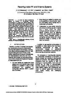
resonator examples are off-chip components. The need for size miniaturization and power minimization leads to the further requirement of single chip integration with active electronics. Potential solutions that can meet these desired specifications employ RF Micro Electro Mechanical Systems (RF MEMS). RF applications of micromachining technology have included micromechanical switches and filters as well as high Q inductors and variable capacitors with wide tunable range that can be combined to form electrical resonators for filtering applications [1]. While MEMS has the potential to support single chip integration, much of the current state-of-the-art MEMS devices have used custom processing, preventing integration with electronics. This paper will describe our recent results in developing CMOS-based mechanically reconfigurable on-chip electrical resonators and electrically selectable on-chip mechanical resonator-mixer arrays and their use in RF circuits that can be used for military spectrum sensing applications. Receiver Architecture A reconfigurable wideband receiver architecture that meets the desired power, Q, tuning range and size for mobile spectrum sensing applications is shown in Fig. 1. The antenna Cdc
Cdc
L
VRFout
VRFin Ctank
Ctank
100 MEMS mixer-filter array
100 kHz
100 MHz
100 MHz
0 fr1 5
fLO
10 GHz tunable BPF
VCC
LMEMS
LO+
Vtune
LMEMS
CMEMS
CMEMS
Cdiv1
Cdiv1
Cdiv2
R
R
Cdiv2
LO-
50 MHz 100 kHz
0 frN 5
50 MHz
0 5
50 MHz
fLO wide-range synthesizer
Vb Ibias
Figure 1. RF MEMS enhanced wideband receiver
receives signals in a very wide band, 100 MHz to 10 GHz, spectrum. A mechanically reconfigurable bandpass filter (BPF) selects 100 MHz of the incoming spectrum around the local oscillator (LO) frequency, fLO. To enable simultaneous control of the BPF and LO signals, the LO signal is generated by a MEMS voltage-controlled oscillator that also uses a mechanically reconfigurable MEMS LC resonator. Coarse frequency hopping to select a band for spectrum analysis can therefore be accomplished by simultaneously retargeting both the VCO and the BPF.
components have both high Q (lower series loss) and higher operating frequencies (lower interconnect parasitics).
The BPF output signal is amplified by a wideband low noise amplifier (LNA), which drives an array of MEMS mixer filters. The mixer-filter array is a manufacturable monolithic implementation of the system vision set forth in [2]. Each of the N mixer-filter in the array downconverts GHz input signal to a unique intermediate frequency (IF), fr1 and frN, set by the mechanical device resonance to be in the MHz range with a 100 kHz filter bandwidth. These mixers simultaneously downconvert from GHz, and with an appropriate IF switching network, act in composite as a fine-hopping filter to analyze the spectrum channel utilization in the band being analyzed.
The CMOS-MEMS variable capacitor is formed by sidewall parallel-plate electrodes from an interdigitated beam array. Micromachining of the dielectric and Si substrate enables one set beams to move with respect to the other under electrothermal microactuation [5]. Although substantial heater power is needed when changing capacitance, zero power is required to hold the capacitor at a fixed value through the use of a friction clutch mechanism. The clutch is normally engaged to the moving electrode frame by exploiting selfassembly from the lateral residual stress gradient designed into the actuator beams and is disengaged through electrothermal control. Capacitance tuning ratios of 5:1 have been demonstrated, with the potential for 9:1 being developed.
Post-Foundry Micromachining Monolithic integration is enabled by micromachining the passive hardware components following foundry CMOS or BiCMOS wafer manufacture [3]. Structures are micromachined from the metal and dielectric layers manufactured by the foundry using a sequence of dry etch steps as shown in Fig 2. In addition to high fT transistors, advanced foundry processes offer several advantages in RF MEMS microstructure fabrication compared to the older foundry processes used for sensor fabrication [3]. Firstly, the improved stress matching from larger wafers combined with the thicker microstructures arising from the larger number of metal layers combine to reduce out-of-plane curl. Secondly, the reduced minimum metal spacing rule enables the design of smaller gaps. Furthermore, RF CMOS-MEMS passive components are constructed using thick RF foundry metallizations, while existing RF MEMS devices tend to use lossy silicon-based materials [2]. Thus RF CMOS-MEMS passive CMOS microbeam metal-3 FET structures metal-2 polysilicon metal-4 metal-1
anchored stator
RF MEMS L and C The CMOS-MEMS inductor is based on the classical RF spiral inductor. The anisotropic dielectric etch shown in Fig 2(b) removes the dielectric between the metal inductor turns increases self-resonance by 2x. The combined sacrificial Si etch shown in Fig 2(c) removes 30 to 50 µm of lossy silicon under the turns improving inductor Q by 1.5x [4].
RF MEMS Circuits The RF BPF consists of a low-pass Butterworth network consisting of MEMS inductors and capacitors with dc blocking capacitors to reject low frequencies [4]. The reconfiguration capability of the filter is achieved solely from the reconfigurable capability of the CMOS-MEMS variable capacitors. Fig 3 shows the transmission gain indicating that the filter can be reconfigured between flow = 1.87 GHz (with the MEMS capacitors at their maximum value) and fhigh = 2.36 GHz (capacitors at minimum value). Filter insertion loss depends on capacitance ratio. Controlling this ration in simulations predicts that this topology can achieve an insertion loss as low as 6 dB. In the experimental measurements, the capacitors could not be controlled independently. The third measured curve in Fig 3 shows that 0 Insertion loss as low as S21 [dB] 7.1 dB have been measured -10 -20 -30 -40
(a) (b) (c) Figure 2. Cross-section of CMOS-MEMS process [3]; (a) foundry CMOS, (b) after anisotropic etch, (c) on final release using a combination of anisotropic silicon DRIE and isotropic silicon etch.
1
flow fhigh 2
3
4 5 6 Frequency [GHz] Figure 3. Filter Transmission Gain showing reconfiguration from flow to fhigh, as well as lowest measured insertion loss of 7.1 dB.
Curl-matched electrode supports
CMEMS
LMEMS
CMEMS Cantilever
Cross-coupled diff pair
VA Drive Electrode VC Resonator electrodes
Figure 4. SEM of reconfigurable MEMS VCO. insertion loss as low as 7.1 dB can be achieved using this fully integrated RF MEMS circuit. Such insertion loss values are comparable to those achievable in many discrete filters. This circuit also demonstrates the first time multiple MEMS capacitors have been integrated with MEMS inductors. Increasing integration of RF MEMS passive components will enable integration of multiple resonators and coupling elements to form true bandpass filters, thereby decreasing insertion loss. Furthermore, classical LC filter design methodologies that include placing of transmission nulls can lead to improved filter Q. In terms of filter reconfiguration range, the widest observed range to date has been 2.6 GHz to 3.45 GHz (850 MHz). This purely passive circuit requires no quiescent power during operation. The MEMS VCO uses a cross-coupled SiGe HBT pair to cancel losses in the tank composed of MEMS inductors and capacitors [6], as shown in Fig 4. The tank consists of a micromachined 6.25 nH symmetrical inductor and MEMS capacitors that can switch between 180 fF and 1 pF. Analog tuning can still be used to arbitrarily control the gap between the fingers. By engaging the clutch during VCO operation, the VCO only sees a constant gap between the fingers, preventing the adverse impact of capacitance nonlinearity and Brownian motion noise on the VCO phase noise. This VCO had a measured phase noise of -122 dBc/ Hz at 1 MHz offset from the 2. 8GHz carrier with a core current of 1.1 mA from a 2.5 V supply. This results in a figure of merit (FoM) of 187 dB. This VCO required 5x less power than other comparable VCOs in the literature, due to loss reduction from the MEMS LC tank on-chip next to the transistors. In addition to the excellent figure of merit in comparison to VCOs that use on-chip spiral inductors, the VCO is also reconfigurable, just like the band pass filter [4]. To date, the largest reconfiguration range achieved has been 2.07 GHz to 2.84 GHz, with the MEMS capacitance being aided with an analog diode varactor (designed for ~100 MHz of tuning range). The highest oscillation frequency generated to date has been 4 GHz. Mixer Filters MEMS resonator mixer filters are micromechanical devices that exploit the V2 nonlinearity of the electrostatic force [7].
Sense electrode
Figure 5. SEM of a single two-metal-layer CMOS cantilever resonator, with an electrode square on the end and curl-matched drive and sense electrodes. Mixing and IF filtering may be accomplished in a 0.02 mm2 area with less than 1 mW power, driving the potential for large parallel tuning arrays for the spectrum sensor. Initial RF CMOS MEMS mixer-filters have been made from cantilever beams. The cantilever in Fig 5 has a resonant frequency of 435 kHz and a Q of 1440, measured at 100mTorr. Application of an RF signal to the stationary electrode and the LO signal to the cantilever generates an electrostatic force at a frequency of ( f RF – f LO ) . Vibration within the cantilever’s mechanical resonance band is amplified by the mechanical Q and read out capacitively through the IF electrode using a preamp. A downconverting mixer can be made using two such cantilever resonators wired in a differential topology to for low RF feedthrough as shown in Fig 6. Successful mixing with these resonators has been observed up to 3.2 GHz input frequencies [8]. The limiting factor in arbitrarily increasing this frequency has been RF reflections in the PCB testboard. Besides nearly trivial integration with CMOS circuits, CMOS MEMS offers the freedom to route different electrical signals on the multiple electrically isoAoffchip Vout Aonchip
fRF
fLO VP+
VP-
Figure 6. SEM image of differential cantilever resonators with an overlaid circuit schematic for operation as a mixer-filter.
PB
P1
VBias
RHP
VBias
P2 = (A-1) P1
Q3 = Q1
Acknowledgements
RF IBias
v IN
vOUT1
RS vIN
CHP
Q1
Path 2
VCO, a mixer-filter with sub-mW power, and a wideband LNA that can be fabricated on the same die have been described.
vOUT
Path 1 Q2 = A*Q1
Figure 7. Noise-canceling wideband LNA. lated conductive layers within the moving mechanical resonator. Currently, the overall conversion loss in downconverting and filtering RF signals is 50 dB. Combining an improved capacitive readout preamp design (still with sub mW power) with narrower resonator gaps of 400 nm (that have previously been successfully fabricated) has the potential to offer 0 dB conversion gain. Wideband LNA A wideband LNA is needed to amplify the signal from the reconfigurable bandpass filter and drive the RF signal into the array of mixer-filters. Wideband LNAs tend to suffer from low noise figure. To overcome this, a two-stage noise cancelling wideband LNA inspired by [9] has been designed in the same SiGe foundry process as the BPF, VCOs, and mixer-filters. Fig 7 shows the overall circuit. By matching the gain of the two paths from the first stage output (labelled VOUT1) to the second stage output (labelled VOUT), the topology ensures that the maximum possible amount of noise generated by the first stage (Q1 and P1) is cancelled. This optimization was done using the DARPA NeoCAD supported UltraSYN synthesis tool suite. The resulting design (occupying 70µm x 90µm) has a measured S21 of 17 dB and a -3 dB frequency of 2.64 GHz. The minimum Noise Figure (NF) is 2.4 dB and the NF is less than 3 dB for entire 3 dB bandwidth. The circuit has a measured IIP3 of -1.14 dBm (obtained using two tones, at 1.5 and 1.505 GHz). The ICP was -16.5 dBm at 1.5 GHz. All these measurements were taken with circuit biased at 13 mA from 2.5 V supply. Conclusions Spectrum sensors are of interest not only for adaptive radio communication, but also for electronic listening. The ability to integrate high Q electrical and mechanical resonators, with reconfiguration at GHz frequencies and array-based selection at MHz frequencies in a post-foundry micromachining platform meets all the desirable characteristics for spectrum sensors: low power, frequency agility, single chip integration. First generation circuits for a spectrum sensor architecture have been demonstrated. In particular, a reconfigurable zero-power BPF, a low-power reconfigurable
This research effort was supported by C2S2, the MARCO/ DARPA Focus Center for Circuit & System Solutions, under MARCO contract 2003-CT-888 (PM: Dan Radack), by the DARPA NMASP program under award DAAB0702-C-K001 (PM: Dan Radack) and DARPA NeoCAD program under award F33615-01-2-1970 (PM: Anantha Krishnan). References [1] C. T.-C. Nguyen, L. P. B. Katehi, G. M. Rebeiz, “Micromachined devices for wireless communications,” Proc. of the IEEE, vol. 86, Aug. 1998, pp. 1756–1768. [2] C. T.-C. Nguyen, “Vibrating RF MEMS for Next Generation Wireless Applications,” Proc. IEEE CICC, pp. 257-64, Oct. 2004. [3] G. K. Fedder, S. Santhanam, M. L. Reed, S. C. Eagle, D. F. Guillou, M. S.-C. Lu, and L. R. Carley, “Laminated High-Aspect-Ratio Microstructures In A Conventional CMOS Process,” Sensors & Actuators, vol. A57, no. 2, pp. 103-110, March 1997. [4] D. Ramachandran, A. Oz, V. K. Saraf, G. K. Fedder and T. Mukherjee, “MEMS-Enabled Reconfigurable VCO and RF Filter,” Proc. 2004 IEEE RFIC Symposium, Ft. Worth, TX, June 6-8, 2004, pp. 251-254. [5] A. Oz and G. K. Fedder, “CMOS/BiCMOS SelfAssembling and Electrothermal Microactuators for Tunable Capacitors, Gap-Closing Structures and Latch Mechanisms,” Technical Digest of the 2004 Solid-State Sensor, Actuator and Microsystems Workshop, Hilton Head Is., SC, pp. 212-215. [6] V. K. Saraf, A. Oz, D. Ramachandran, G. K. Fedder and T. Mukherjee, “Low-Power LC-VCO using Integrated MEMS Passives,” Proc. 2004 IEEE RFIC Symposium, Ft. Worth, TX, June 6-8, 2004, pp. 579-582. [7] A. Wong, C. T.-C. Nguyen, “Micromechanical mixerfilters,” J. Microelectromech. Syst., vol. 13, no. 1, Feb. ‘04, pp. 100. [8] F. Chen, J. Brotz, U. Arslan, C.-C. Lo, T. Mukherjee, G. K. Fedder, “CMOS-MEMS Resonant RF Mixer-Filters,” Proc. IEEE MEMS 2005, Miami, FL, Jan 30-Feb 3, 2005, pp 24-27. [9] F. Bruccoleri, E. A. M. Klumperink, and B. Nauta, “Wide-band CMOS low-noise amplifier exploiting thermal noise canceling,” IEEE Journal of Solid-State Circuits, SC-39(2), Feb. 2004, pp. 275-282.