Run-control and service element code simulation for the SI390 microprocessor
by S. Koerner S . M. Licker
In recent years the importance of time to market for new computer systems has grown. Very little time can bespent in hardware bring-up and the system integration phase when new hardware and new code (several megabytes) come together for the first time on the test floor.This paper describes some of the measures that were taken to achieve this goal on the S/390@Parallel Enterprise Server Generation 4.
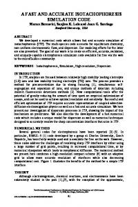
procedure also includes loading of the I/390 (maintenance and I/O) code [l(a)] as well as resetting and initializing the storage elements in the system. These tasks are accomplished by a service processor connected to the S/390 system. Typically the service processor is a Thinkpad* running OS/2* and the service element code (SE code); see Figure 1. The dataflow between the service element and the S/390 system is issued from the SE code via the parallel port of the Thinkpad. It interfaces by means of a universal power controller card (UPC) with the central clock-generation chip (CGC). The run-control portion of the central clock-generation chip comprises the hardware center of control for the S/390 processor complex. The connection between the universal power controller card and the clock-generation chip is an asynchronous five-wire serial interface. To achieve a fast hardware bring-up time [l(b)], these components must be verified by simulation before first power-on. This has been done successfully for the last four S/390 CMOS processor complexes. The setup described in this paper was developed in Boeblingen for CMOS-based S/390 systems in 1991, and has been used most recently by IBM Poughkeepsie for the S/390 Parallel Enterprise Server Generation 4.
Introduction The current S/390* microprocessor design points from Boeblingen and Poughkeepsie are microcode/millicodebased implementations of the S/390 architecture using level-sensitive scan design (LSSD) design rules. The microcode/millicode is resident either in read-only storage (ROS) or in random-access memory (RAM) in the central processing unit (CP). The microcode/millicode routines, which are very timing-critical, are permanently stored in the ROS part of the CP, but to make the system operational, significant portions of that code must be loaded after power-on into the RAM. This "bring-up"
"Copyright 1997 by International Business Machines Corporation. Copying in printed form for private use is permitted without payment of royalty provided that (1) each reproduction is done without alteration and (2) the Journal reference and IBM copyright notice are included on the first page. The title and abstract, hut no other portions, of this paper may be copied or distributed royalty free without further permission by computer-based and other information-service systems. Permission to republish any other portion of this paper must he obtained from the Editor.
W l & W 9 7 & 5 . W 0 1997 IBM
IBM J. RES. DEVELOP. VOL. 41 NO. 415 JULY/SEPTEMBER 1997
S. KOERNER AND S. M. LICKER
UPC card generation
complex
I ThinkPad running OS/2 and service element code
a
Physical S/390 system structure.
Software simulation model (central clock generation S/390
UPC high-level model
\
t Test-case interpreter
because self-test is performed for all chips as well as for the startistop clock, scan-ring shifting, the serial link, single-cycle microinstruction step generation, and X-reg communication. The run-control simulation is based on shifting data into the clock-chip chains (scan-ring shifting) and the other Si390 processor chips using the HIMO of the UPC card. In an LSSD design, all latches in a single chip are part of one chain and can be accessed by shifting of the entire chain. This is the primary control mechanism into the Si390 processor. In the interpreter environment, all simulation model elements are accessible for test and set to establish regression capability. These types of tests comprise 100 000 lines of code and verify the underlying hardware by removing errors to an extent that enables a fast hardware bring-up. The total elapsed simulation time to run all tests is about 200 hours on an Si390 system (9672-RX3); see Figure 2. The simulation runs in an Si390-based computing center, parts of which are dedicated to the SE code and run-control simulation. The simulator, MLDVS, is a tool developed in Boeblingen. MLDVS (medium-level design verification simulator) is an event-driven simulator which is especially well suited for asynchronous types of simulation as they appear in the run-control logic. The intent of the first step in the verification process is to find all hardware-related run-control problems prior to release of the chips to manufacturing.
SE code simulation
Verification strategy The verification strategy is based on a two-step approach and is quite different from the CP verification methodology. There is no test strategy with random testcase generators. All tests are deterministic, with a wellknown scope of functions being verified.
Run-control simulation
578
In the first step, the run-control logic is verified on a bitlevel basis using a simplified representation of the UPC card as a high-level model (HIMO) [l(c)]. The bit-level verification uses a language developed especially for verification of Si390 run-control logic. The syntax elements of this language are as follows: shift data into the Si390 processor; compare shift data; set and test facilities and conditional branches. To allow quick changes in any test case without spending compile time, this test language is interpreted by a program called IRESA (interpreter for run-control, error simulation, and array built-in self-test). It allows the simulation of all run-control functions
S. KOERNER AND
S. M. LICKER
Step two of the verification process verifies the correctness of the interaction between the hardware model verified in step one and the SE code. The SE code simulation is not targeted to find hardware problems, but rather software and specification errors. Specification errors are found primarily in the area of accessing processor internal arrays and in the engineering data file. The functionality of the SE code covers initial microcode load (IML), initial program load (IPL), Si390 manual operations, and error detection and isolation. All of these functions use the runcontrol interface into the Si390 processor complex. As stated above, the Si390 processor must have microcodeimillicode and I/390 code to become operational. The underlying SE code that transfers the code incorporates the basic hardware access mechanism to access array and storage elements and knowledge about the physical structure of the Si390 system. The structure of any chip is reflected in its engineering data file. The engineering data file, which describes the sequence of latches and storage elements on the scan ring of every chip, is part of the SE code.
IML The task of loading the code into the Si390 processor complex is called initial microcodeimillicode load (IML);
IBM J. RES. DEVELOP. VOL. 41 NO. 415 JULY/SEPTEMHER 1997
two different methods are used to transfer the code into the Si390 processor. In the first steps of IML on the Si390 Parallel Enterprise Server G3, about 1000 bytes of bootstrap microcode is loaded into the CP control store array via the CP-chain interface. On the Si390 Parallel Enterprise Server G4, a fast load sequence shifts the bootstrap millicode data into the L2 cache array via a buffer register. The SE code scans the data into the arrays using special array access routines. On the G4, these array access routines were verified in simulation by using the test and debug monitor (TDM) alteridisplay to write and read the arrays in the CP and L2 and then verify the correct results in the simulation model. This capability was also used to assist in the reproduction and debug of problems from the engineering test floor. The next steps in the IML process are to transfer the large amount (several megabytes) of microcodeimillicode and I/390 code into the machine by using the X-reg communication. The X-reg communication establishes a fast link between the CP microcodeimillicode that was loaded in the first steps of IML and the SE code. Since this is a critical item for the system integration, it is verified in great detail on the design level (see step one of the verification process) and with the SE code simulation. In SE code simulation, the actual shift interface cannot be used for performance reasons because the actual shift speed is between 0.1 bitis and 1 bitis for the MLDVS software simulator. Since a typical CP chain is more than 50 000 bits long, this would lead to an unacceptably long simulation time frame. Instead of scan-ring shifting, therefore, the data are broadcast into the simulation model, resulting in a speed improvement factor of 1000 through circumventing the scan-ring shift mechanism. The actual scan-ring shifting process is simulated with the use of other test methodologies. (See the paper in this issue by Wile, Mullen et al. [2] on functional verification of the S/390 Parallel Enterprise Server G4.)
Hypervisor The controlling element in the SE code simulation setup is the hypervisor. This program is the supervisor for the simulation process; it takes the data from the SE code and puts them into the simulation model, lets the simulation run, and returns data from the simulation model back to the SE code. The hypervisor was coded in REXX and interfaces with both the simulation model and the SE code. In the SE code simulation setup, the SE code is run on a PS/2* connected to the VM software simulator. The protocol between SE code and VM is SRPI (server requester protocol interface). For the SE code, there is no difference between simulation and the real hardware. On the VM side, CMSSERVE (a workstation server program) is running. Because VM is a single-tasking operating
IBM J. RES. DEVELOP.
VOL. 41 NO. 4/S JULY/SEPTEMBER 1997
Atlantic Ocean 4
VM running
ThinkPad running SE code IBM Boeblingen S/390 simulator system Poughkeepsie IBM
hypervisor and software
system, a second VM machine is needed for simulation to run the MLDVS simulator and the hypervisor for the Si390 Enterprise Server G3 and the ZFS simulator for the S/390 Enterprise Server G4. The two VM virtual machines are connected via IUCV (interactive user communication vehicle). The amount of data transferred back and forth between the SE code and the hardware model is less than 100 bytes or more than 10 kilobytes, depending on the type of SE operation currently performed. This simulation depends heavily on the uniprocessor performance of the software simulator. In Boeblingen’s SE code simulation, the PSI2 with the SE code was located in Boeblingen, and the software simulator was on a 9672-RX3 system in Poughkeepsie (this was the most powerful Si390 system available for simulation in that time frame); see Figure 3. The mean time between failures in this complex simulation environment during a running simulation was about 12 hours (mostly network problems). This was the limiting factor in the scope of simulation. In principle, with this type of setup, a complete IML can be verified; considering the actual simulation performance, only the most basic but important functions were verified. The total number of cycles necessary to simulate a complete IML is more than 50 000 000 cycles. This had been done with the EVE 1.5 and EVE 2.0 hardware simulators in Poughkeepsie for the H series of processors. The problem in this area is not only having simulation “horsepower,” but also being able to build a simulation model with all required system elements, including the I/O subsystem, that will fit on the EVE simulator. The time available within the development cycle to do this type of
S. KOERNER AND S. M. LICKER
simulation is extremely short. Because the SE code incorporates the engineering data, the hardware model must be quite stable in order to generate the code and still have a valid hardware representation for simulation. Typically this type of simulation starts after release of the S/390 chips to manufacturing and lasts until the first steps of hardware bring-up. As a result of the run-control and SE code simulation, the last four CMOS systems (including the G4) had only minor problems in the area of run control and IML. Another use of the SE code simulation environment on the G4 was the verification of a stand-alone bring-up configuration. The G4 bring-up strategy was to test initially with a configuration of only the clock, CP, and L2 chips; memory and 1/0 were not in the configuration. A special test environment was set up to deliver SAK (systems assurance kernel) test cases from an S/390 host system to the service element and into the L2 cache. The CP then executed the test case, and the results were read out by the service element and sent back to the S/390 host to be verified. The delivery system and test-case execution were verified completely using the SE code simulation environment.
Summary Therun-controlhardwareteststrategy is toconcentrate on areas that are vital for the control of the S/390 processor complex and to verify the related hardware functions carefully to ensure that the fast bring-up of the system On the engineering test floor is not jeopardized. The SE code test strategy is to verify the basic code layers that are being used by the SE code each time it accesses the hardware. Verification of these code layers depends on the simulation horsepower and the establishment of a process to ensure that the appropriate code level is available to match the final level of hardware.
References W. Spruth, H. Kriese, J. Maergner, and H. Schwermer, The Design of a Microprocessor, Springer-Verlag Berlin, 1989: (a) J. Maergner and H. Schwermer, p. 303; (b) W. Hehl, p. 316; (c) H. Kriese, p. 184. 2. B. Wile, M. P. Mullen, C. Hanson, D. G. Bair, K.M. Lasko, P. J. Duffy, E. J. Kaminski, Jr., T. E. Gilbert, S. M. Licker, R. G. Sheldon, W. D. Wollyung, W. J. Lewis, and R. J. Adkins, “Functional Verification of the CMOS S/390 Parallel Enterprise Server G4 System,” ZBM J. Res. Develop. 41, No. 4/5, 549-566 (1997, this issue). 1.
Received December 18, 1996; accepted for publication August 13, 1997
Stefan Koerner IBM Entwicklung GmbH, Schoenaicherstrasse 220, 71032 Boeblingen, Germany (KOERIVER at BOEVM4). Mr. Koerner is an Advisory Engineer in the S/390 hardware development organization in the Boeblingen laboratories. He joined IBM in Boeblingen in 1981 and has held a number of positions in logic design,
microcode development, and design verification. He was the technical team leader in the area of S/390 run-control, IML, and microcode simulation for the S/390 G3 systems. Mr. Koerner holds one patent and received an IBM Hardware Development Team Award in 1996.
Steven M. Licker ZBM System1390 Division, 522 South Road, Poughkeepsie, New York 12601 (
[email protected]). Mr. Licker is an Advisory Engineer working in IBM S/390 design verification. He joined IBM in 1977, and has held a number of technical and management positions in engineering systems testing on the IBM 308X and 3090 projects. Mr. Licker has spentthe last ten years doing processor and system simulation on the IBM ES/9000 and S/390 G4 systems. He received an IBM ‘ k a m Award for SI390 G3 COmmon chip verification in 1996.
Conclusion Without the different steps in verification of the runcontrol logic and the SE code, fast hardware bring-up and system integration times (one new CMOS generation every year) are not achievable. Because the development community in IBM is using primarily RS/6000* tools for simulation and chip development, the hypervisor and IRESA will be coded in C and connected via TCP/IP to the PS/2. The hypervisor will support simulation as well as emulation on different target systems. The future will bring additional effort in this area, with improvements in the development process and in simulation and emulation horsepower to further reduce the time needed for hardware and system bring-up.
580
*Trademark or registered trademark of International Business Machines Corporation.
S. KOERNER AND S. M. LICKER
ISM J. RES. DEVELOP.
VOL.
41 NO. 415 JULYiSEPTEMBER 1997