reconfigurable logic, for a new application to be implemented the whole chip ... is a configurable architecture that allows the user to construct custom application-.
SPS: A STRATEGICALLY PROGRAMMABLE SYSTEM S. Ogrenci- Memik, E. Bozorgzadeh, R. Kastner, and M. Sarrafzadeh Computer Science Department University of California-Los Angeles, CA Abstract We are presenting a novel reconfigurable system architecture: the Strategically Programmable System (SPS). The motivation for such a system is the needs of today’s high flexibility, high performance computing. SPS contains versatile blocks embedded into fully reconfigurable logic. Dedicated blocks fixed on the chip perform the bulk of the computations; hence the reconfiguration time of the system is highly improved as well other performance metrics such as speed and power consumption. Fine grain reconfigurable logic helps maintain high flexibility. 1. Introduction Today’s embedded systems contain various combinations of different sub-systems, such as ASICs, microprocessors, DSPs, and reconfigurable cores. Reconfigurability is added to these systems with either individual FPGA chips or other forms of reconfigurable logic. New embedded systems require a larger amount of flexibility as compared to their predecessors. Markets change very rapidly demanding embedded system solutions that are easily alterable. Reconfigurable cores in embedded systems provide the necessary adaptability. In addition many high performance operations, such as computationally intensive signal processing functions can be implemented very efficiently using reconfigurable logic. Reconfigurable cores are becoming essential elements in embedded systems. Standalone FPGAs are also gaining importance in a similar context. High density FPGAs are available in the market offering competitive solutions to ASICs and programmable systems such as DSPs. New generation of FPGAs have a trend towards embedding coarser grain units. The traditional fine-grain FPGA architectures are shifting towards new architectures where memory blocks, hard IPs, and even CPUs are being integrated into FPGAs. In these designs the traditional FPGA is not a co-processor, instead a reconfigurable fabric is embracing all the mentioned components and enabling a much tighter connection among them [1, 2, 3]. Flexibility in reconfigurable systems comes at the expense of the reconfiguration time. The amount of time required to set the function to be implemented on the reconfigurable logic is the configuration time, which can become a serious bottleneck especially in systems where run-time reconfiguration is performed [4, 5]. We propose a new architecture for a system that uses reconfigurable logic, which we refer to as Strategically Programmable System (SPS). The basic building blocks of our architecture are parameterized functional blocks that are pre-placed within a fully reconfigurable fabric. They are called Versatile Parameterizable Blocks (VPBs). When implementing an application, operations that can be mapped onto these fixed blocks will be performed by the VPBs; computational blocks that will be instantiated on the fully reconfigurable portion of the chip will perform the remaining operations. Properties of VPBs will be discussed in more detail in later sections. Our motivation is to generate reconfigurable architectures that are developed targeting a set of applications. Such architectures would contain VPBs to specially suit the needs of the particular family of applications. Yet the adaptable nature of our programmable device should not be severely restricted. The SPS will remain flexible enough to implement a very broad range of applications thanks to the reconfigurable resources. These powerful features help our architecture maintain its tight relation to its predecessors, traditional FPGAs. At the same time the SPS is forming one of the first efforts in the direction of context-specific programmable devices. Since the VPBs are custom-made and fixed on the chip, they do not require configuration, hence there are considerably less switches to program as compared to the implementation of the same design on a traditional FPGA. More important, an instance of our SPS architecture is generated such that for a given set of applications the suitably selected fixed blocks provide the best performance. In this paper we introduce the basic concepts of our architecture and the notion of generating an instance of the SPS architecture for a given set of applications. We present a framework that provides tools for generating SPS instances and implementing applications once a fixed SPS architecture is given.
In the following section we present related work in the field of reconfigurable architecture. Examples of versatile programmable blocks are presented in Section 3 as well as details of our architecture. We complement our architecture with tools that perform the mapping of applications onto the architecture and the actual implementation and tuning for an application on our platform. These two major tasks will be discussed in Section 4. In Section 5 we present our preliminary results. 2. Related Work There has been considerable research effort for developing reconfigurable architectures in the past. Also there are numerous commercial reconfigurable devices introduced. First programmable devices were standalone chips. With the current trend towards hybrid programmable architectures, new systems with embedded reconfigurable cores are also being developed. Among these architectures the basic distinction is due to the level of granularity of the reconfigurable logic. Commercial FPGAs from several vendors such as Xilinx, Altera, and Actel are available in the market. Traditional FPGA chips like Xilinx 4000 series, or Altera Flex family all contain some form of an array of programmable logic blocks. Those blocks usually are not very complex; contain a few LUTs and a small amount of storage elements. They are designed for general-purpose use. Since they only contain fine-grain reconfigurable logic, for a new application to be implemented the whole chip goes through a configuration phase. Although newer devices such as Xilinx Virtex FPGA allow partial reconfiguration of selected rows or columns, this is still a critical issue. There are also hybrid systems that contain reconfigurable cores as coprocessors. The Garp architecture developed at UC Berkeley combines a MIPS-II processor with a fine-grained FPGA coprocessor on the same die [6]. Unlike the Garp architecture the main load of hardware implementation lies on the coarse grain parameterized blocks in SPS architecture. Chimaera [7] is a single chip integration of reconfigurable logic with a host processor. The reconfigurable coprocessor is responsible for performing the Reconfigurable Functional Unit (RFU) instructions. An RFU instruction is any instruction from the program running on the host processor that is performed by the reconfigurable coprocessor. The Chimaera architecture is for a very specific class of data path applications and still requires a large amount of reconfiguration time. Another reconfigurable architecture with fine-granularity is the Dynamically Programmable Gate Array (DPGA) [8]. Although the logic structure is just like existing FPGAs, DPGAs differ from traditional FPGAs by providing on-chip memory for multiple array configurations. The on-chip cache exploits high, local on-chip bandwidth to perform quick reconfiguration. In addition, several systems with coarse-grain granularity exist, such as RaPiD [9], Raw [10], and Pleiades[11]. RaPiD is a configurable architecture that allows the user to construct custom applicationspecific architectures in a run-time configurable way. The system is a linear array of uncommitted functional units, which contain datapath registers, three ALUs, an integer multiplier and some local memory. The RaPiD architecture targets applications that can be mapped to deep pipelines formed from the repeated functional units. The Reconfigurable Architecture Workstation (Raw) is a set of replicated tiles, where each tile contains a simple RISC like processor, small amount of bit-level configurable logic and some memory for instructions and data. The CS2112 Reconfigurable Communications Processor (RCP) from Chameleon Systems, Inc. [12] contains reconfigurable fabric organized in slices, each of which can be independently reconfigured. The CS2112 includes four slices consisting of three tiles. Each tile comprises seven 32-bit Datapath Units, two 16x24-bit single-cycle multipliers, four Local Store Memories and a Control Logic Unit. The RCP uses a background configuration plane to perform quick reconfiguration. This reconfigurable fabric is combined with a 32-bit embedded processor subsystem. The Pleiades architecture is a processor approach that combines an on-chip microprocessor with an array of heterogeneous programmable computational units of different granularities connected by a reconfigurable interconnect network. The programmable units are MACs, ALUs, and an embedded FPGA. Xilinx has recently introduced the Virtex-II devices from of the new Xilinx Platform FPGAs [1, 2]. The Virtex-II architecture includes new features such as up to 192 dedicated high-speed multipliers. Designers can use Virtex-II devices to implement critical DSP elements of emerging broadband systems. This is somewhat a similar effort in the same direction that we are heading. The Virtex-II device is providing the
dedicated high-performance multipliers for DSP applications like the VPBs on the SPS are intended to improve performance for a set of applications. SPS differs from a Virtex-II device in the following: -
Our architecture can contain blocks of various complexities. Depending on the requirements of the applications fixed blocks can be as complex as an FFT block or as simple as an adder or multiplier. Examples of VPBs will be provided in Section 3.2.
-
The generation of an SPS instance is automated. Given a set of target applications an architecture generation tool determines the number and types of VPBs to be placed on the chip.
-
While the Virtex-II device is still general purpose, an instance of an SPS will be more context-defined according to a given set of applications.
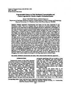
RAM VPB
VPB
RAM VPB Figure 3.1.1 Sample SPS architecture 3. SPS Architecture In this section we present the architecture we are proposing. We will explain the different parts that make up the SPS. Then examples of VPBs will be presented. 3.1 Hardware Components of the SPS Figure 3.1.1 illustrates the concept of our SPS architecture. VPBs, fine grain reconfigurable logic, and memory are presented in this figure. The most important component of our architecture is the parameterized functional block called a versatile programmable block (VPB) or a common block. VPBs enable the system to be flexible, but their basic structure remains fixed on the chip such that the reconfiguration time is no longer a severe limitation. The VPBs can be complex enough to suit a range of applications. They can as well be more basic such as an adder, a multiplier, or an ALU type of a block that can perform multiple operations. Also some features of the blocks can be alterable, such as the word width. Through a programmable routing architecture multiple blocks can be combined to obtain a wider word width component. The fixed blocks are integrated into fully reconfigurable fine grain logic. Functions that cannot be covered by the versatile programmable blocks will be mapped onto that portion of the hardware. On-chip memory blocks are also available for data storage. Programmable interconnect architecture provides an interface between the fixed common blocks and the fully reconfigurable logic, which are also depicted in Figure 3.3.1. 3.2 Target Applications Our first target set is DSP applications. Repetitive arithmetic operations on a large amount of data can be very efficiently implemented using hardware. Our primary examples focus on several image-processing applications. This soon will be extended to cover other types of applications. First, algorithms that have common properties and operations are grouped together. Such algorithms can use a common set of VPBs for their implementation. The algorithms and the classes that they belong to are summarized in Table 3.2.1. Image-processing operations can be classified into three categories. Those that generate an output using the value of a single pixel (point processing), those that take a group of neighboring pixels as input (local
processing), and those that generate their output based upon the pixel values of the whole image (global operations) [13]. Point and local processing operations are the most suitable for hardware implementation, because they are highly parallelizable. We have designed three blocks each representing one algorithm class. The blocks that we are currently considering are described in the following. In Section 5 we will refer to the implementation of these blocks on fully reconfigurable logic vs. the parameterized block realization and present the potential reduction in the number of configuration bits. Table 3.2.1 Our Classification of Algorithms Algorithms Image Restoration, Mean Computation, Noise Reduction, Sharpening/Smoothing Filter Image Halftoning, Edge Detection Image Darkening, Image Lightening
Operations Weighted Sum, addition, subtraction, multiplication
Class Filter Operations
Comparison
Thresholding
Addition, Subtraction
Pixel Modification
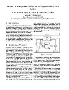
Filter Operations Block: Many signal-processing algorithms are in essence filtering operations. Basically weighted sum of a collection of pixels indicated by the current position of the mask over the image is computed for each pixel. The filter block is currently the most complex block we have designed. It is developed to cover an iterative image restoration algorithm, and several other filtering operations such as, mean computation, noise reduction, high pass sharpening, Laplace operator, and edge detection operators (e.g. Prewitt, Sobel). The block diagram is shown in Figure 3.2.1. Mask coefficients [wi] B
w2
A
w5
w1
w6
w7
w8
w9
In_pixels [pi]
w3
w4 Out_pixel
b c
Figure 3.2.1 Filtering Block The general form of the computation that this block performs is given by the following equations: weighted_sum = Sum{wi x input_pixelI} output_pixel_value = B x input_pixel_value + A x pixel_value_from_prev_iteration – b x weighted_sum + c x weighted_sum This block takes five parameters that define its operation. The mask coefficients array holds the values of the coefficients. Parameters B, A, and c take the value 0 for all the functions except the iterative image restoration algorithm. In_pixel
Out_pixel
255 ALG T
0 Compare
Figure 3.2.2 a. Thresholding VPB
Out_pixel
In_pixel
J ALG
Input routing
Figure 3.2.b. Pixel modification block
Thresholding Block: The operators in this class produce results based on a single pixel’s value. The computation is rather simple, which compares the value of the input pixel to a predetermined threshold value. The output pixel value is determined accordingly. Figure 3.2.2.a illustrates the structure of this block. The parameters of this block are the threshold value T and the algorithm selection input. For the image halftoning application the threshold value, T, is set to be 127, where the pixel vales range between 0(black) and 255(white). If the pixel value is above threshold output is given as 255, otherwise it is 0. For the edge detection operation, the output is set equal to the input value if the pixel value is above threshold, and to 0 otherwise. Pixel Modification Block: Pixel modification operations are point-processing operations. This block performs darkening, lightening, and negation of images. It takes two parameters; J and algorithm selection input ALG. For the darkening operation a positive value J is added to the input pixel value. Lightening is achieved by subtracting J from each input pixel. The negative of an image is achieved by subtracting the input pixel value from J, which takes the value 255 for this case. The block diagram of the pixel modification block is illustrated in Figure 3.2.3.b. 4. SPS Framework In this section we are discussing the tools and algorithms that actually generate strategically programmable systems and perform the mapping of applications on our architecture. The architecture formation phase and the architecture configuration phase are the two major parts of the framework. In Figure 4.1 the SPS Framework is summarized. 4.1 Architecture Formation This task can be described as making the decision on the versatile programmable blocks to place on the SPS chip along with the placement of fine-grain reconfigurable portion and memory elements, given an application or class of applications. In this phase, SPS architecture is customized from scratch given certain directives. This process requires a detailed description of the target application as an input to the formation process. A tool will analyze these directives and generate the resulting architecture. Again the relative placement of these blocks on the SPS chip along with the memory blocks and the fully reconfigurable portions need to be done by our formation tool. Unlike a conventional fine-grain reconfigurable architecture, on the SPS chip the uniform distribution of configurable logic blocks does not exist anymore. Hence for an efficient use of the chip area as well as high performance, the placement of VPBs on the chip and the distribution of configurable logic block arrays and memory arrays among those are critical. The routing architecture that should support such hybrid architecture is equally important and requires special consideration. If the routing architecture cannot provide sufficient routing resources between the s and the configurable blocks, the hardware resources can be wasted. The type and number of routing tracks and switches need to be decided such that the resulting routing architecture can support this novel architecture most efficiently. The most important issues here are the routability of the architecture and the delay in the connections. 4.2 Fixed Architecture Configuration Another case that we are considering in our work is mapping an algorithm onto a given architecture. At this point we need a compiler tailored for our SPS architecture. This SPS compiler is responsible for three major tasks: - The compiler has to identify the operations, groups of operations or even functions in the given description of the input algorithm that are going to be performed by the fixed blocks. Those portions will be mapped onto the VPBs and the information regarding the setting of the parameters of the VPBs will be sent to the SPS chip. - Secondly, the SPS compiler will decide on how to use the fully reconfigurable portion of the SPS. Based on the information on the available resources on the chip and the architecture, mapping of suitable functions on the fine-grain reconfigurable logic will be performed. Combining these two tasks the compiler will generate the scheduling of selected operations on either type of logic. - Finally, memory and register allocation need to be done. An efficient utilization of the available RAM blocks on the SPS has to be realized.
Application Classification
VPB Library Manufacturer
Placement
VPBs
Reconfigurable Logic
C program Embedded Memory High Level Synthesis
Mapping onto VPBs
Mapping onto reconfigurable unit
Routing Architecture Scheduling / Allocation
CAD Tool
User
High-Level Application
Placement & Routing
High-Level
Configured SPS Figure 4.1 Strategically Programmable Systems Development and Implementation Flow 5. Experiments In this section we are presenting our experiments to estimate the potential gain in reconfiguration time that our SPS architecture will yield. We are basically exploring the reduction in reconfiguration bits that would follow as a result of providing pre-placed computation blocks with our coarse grain architecture. 5.1 Application Profiling First we have done a profiling on our image processing benchmarks to gain insight into what type of components are used more frequently. Such a profile can give directives to the architecture formation tool and guide it to employ certain blocks. Looking at the numbers and types of components that were selected by our scheduling tool we have obtained the component usage profile as shown in Figure 5.2.1a. We will create the first version of our experimental SPS architecture given the directives from the profiling information. According to Figure 5.2.1.a the most popular component is the adder with an average of approximately 14 adders per benchmark. Some components such as the 8-bit multiply and bit-wise could not average over 1. These components can be eliminated and we will focus on the rest and decide how many of each of the remaining ones to use on the SPS. If we normalize the numbers according to the constant multiplier, for each constant multiplier there would be one comparator, one subtractor, two right shifters, two left shifters, and seven adders. In the next section we will use this information and estimate the gain of fixing different numbers of components on the chip. Our start point will be the relative usage values given by our analysis. 5.2 Reconfiguration Time In the ideal case the pre-placed blocks should cover all the operations in our target applications such that we can fully exploit the benefits of the custom designed high-performance blocks and improved reconfiguration time. In reality it is not possible to create such an architecture that would support every operation that might be encountered in a wide variety of applications. Hence, in cases where provided blocks are not adequate, extra components are instantiated on the reconfigurable fabric. Here, we evaluate the gain that the VPBs would bring to the configuration process. Our scheduler uses the blocks that are made available and as many additional components as necessary for the best latency. As a result it produces an assignment of the operations to the hardware resources.
% reduction in configuration time
bitwise and
8-bit multiply
compare
shift right
add
average usage
120
16 14 12 10 8 6 4 2 0
100 80 60 40 20 0 intial hardware
doubled
quadrupled
components
Architecture Setups
Figure 5.2.1a. Component utilization profile
50 % increased from previous
Figure 5.2.1b. Potential reduction in configuration (each line representing a benchmark)
time
We are comparing the implementation of the same design on two architectures; a traditional fine grain FPGA and a SPS. We are fixing certain blocks on the SPS assuming they are pre-placed blocks on the chip. These blocks will be our gain in reconfiguration time if they are used by the given application. We are modeling the potential gain in configuration time by assuming that the number of configuration bits is proportional to the amount of logic to be implemented on the reconfigurable fabric. The higher the contribution of the pre-placed blocks is to the total design, the more reduction in reconfiguration time is achieved in this way. Initially we have evaluated an architecture, which contains low-level blocks such as adders, subtractors as explained in Section 5.1. We provide a set of functional blocks fixed on the chip to our scheduler for operation assignment. The scheduler decides on the types and numbers of additional components if they are needed. The first experiment fixes seven 8-bit adders, one 8-bit subtractor, two right shifters, two left shifters and one constant multiplier. Then we have doubled the amount of hardware fixed in proportion at each step except the last one, where we have increased the fixed hardware 50 % from the previous setup. Figure 5.2.1.b presents the relative gains in configuration times for different setups. We observe how the gain in reconfiguration time improves with more logic provided, and how this trend saturates at a certain point. For our initial architecture setup the average reduction in reconfiguration time is 35 %. We observe that as resources available on the chip are duplicated this reduction goes as high as 75 %. If a VPB can cover all operations of an application, then the largest gain can be obtained. Our image processing blocks presented in Section 3 will serve this purpose. They are capable of supporting several different image-processing applications. For the three blocks that we are initially considering, the potential savings in the number of programming bits is shown in table 5.2.1. We have synthesized three parameterized designs for these blocks and obtained area information. Using the CLB count for these blocks we can estimate the number of programming bits required proportional to the size of the designs just as we did for the first set of experiments. We assume that the reconfigurable fabric is similar to a Virtex chip. By using the numbers reported in [14] we derive the number of programming bits required per CLB and hence per parameterizable block. Table 5.2.1 Programming bits required implementing the VPBs with reconfigurable logic Parameterizable Block Size (CLBs) Programming Bits Pixel Modification 30 29,910 Thresholding 11 10,967 Filtering 99 98,703 6. Conclusions In this paper we have presented a novel reconfigurable architecture. Our Strategically Programmable System can provide the degree of flexibility required in today’s systems. While offering high-performance for its application set and still a high degree of flexibility for other applications, our architecture promises a very good performance in terms of reconfiguration time as well. Experiments indicate that a proper
selection of common blocks among a fairly wide range of applications can yield an average reduction of 35 % up to 100 % in the number of programming bits that need to be transferred to the chip for configuration/reconfiguration. Since the VPBs eliminate a considerable amount of programming switches on the chip, the improvement in delay will be accompanied by improved power consumption as well. The individual VPBs will be designed targeting best performance in terms of delay and power consumption. Implementation of applications that are within the covering region of our system will highly benefit from these abilities. 7. Future Work We need to develop the automated architecture formation tools and the high-level synthesis tool in order to complete the SPS framework. The concepts of these CAD tools will be more detailed and a complete system with a set of supporting tools will be developed. We are also planning to manufacture a chip, which will be the product of the automated architecture generation. In this paper we have presented the main concepts of our system. The implementation details and specialized algorithms for our customized CAD tools will be developed as a future work.
References [1] Xilinx Inc., “Xilinx Virtex-II FPGAs Launch New Era of Digital Design”, Press release, January 15, 2001 [2] Xilinx Inc., “ Xilinx Announces DSP Algorithms, Tools and Features for Virtex-II Architecture”, Press Release, November 21, 2000 [3]Altera Corp.,“Excalibur Embedded Processor Solutions”, URL: http://www.altera.com/html/products/excalibursplash.html [4] Ray Bittner and Peter Athanas, "Wormhole run-time reconfiguration", Proceedings of the 1997 ACM fifth international symposium on Field-programmable gate arrays, 1997, pp. 79 - 85 [5] J. G. Eldredge and B. L. Hutchings, "Run-Time Reconfiguration: A Method for Enhancing the Functional Density of SRAM-Based FPGAs", in Journal of VLSI Signal Processing, Volume 12, 1996. [6] J. R. Hauser and J. Wawrzynek, "Garp: A MIPS Processor with a Re-configurable Co-processor," Proc. of the IEEE Symposium on FPGAs for Custom Computing Machines, 1997 [7] S. Hauck, T. W. Fry, M. M. Hosler, J. P. Kao, "The Chimaera Reconfigurable Functional Unit" , IEEE Symposium on FPGAs for Custom Computing Machines, pp. 87-96, 1997. [8] E. Tau, D. Chen, I. Eslick, J. Brown and A. DeHon, "A First Generation DPGA Implementation," FPD95, Canadian Workshop of Field-Programmable Devices, May 29-Jun1, 1995 [9] C. Ebeling, D. Cronquist, and P. Franklin, "Configurable Computing: The Catalyst for HighPerformance Architectures," Proc. of IEEE Intl Conference on Application-specific Systems, Architectures and Proc., July 1997, pp. 364-72 [10] E. Waingold et al, "Baring it all to Software: The Raw Machine," IEEE Computer, Sep 1997. [11] H. Zhang et al., " A 1V Heterogenous Reconfigurable Processor iC for Baseband Wireless Applications", ISSCC [12] Chameleon Systems, Inc., www.chameleonsystems.com. [13] B. Wilkinson, M. Allen, Parallel Programming, Prentice Hall 1999. [14] Xilinx, Inc., “Virtex FPGA Series Configuration and Readback”, Application Note: Virtex Series.