IEEE Computer Society Annual Symposium on VLSI
Standard Cell Like Via-Configurable Logic Block for Structured ASICs Mei-Chen Li, Hui-Hsiang Tung, Chien-Chung Lai, Rung-Bin Lin* Computer Science and Engineering, Yuan Ze University 135 Yuan-Tung Road, Chung-L, Taiwan
[email protected]* the same transistors in CLBs can be used to implement combinational logic and sequential elements. As one can see, most vendors choose metal programmability for cells and routing fabrics. Such a choice incurs a least amount of efforts for tool development. For example, a placer and a router for standard cell designs can be customized for this kind of structured ASICs. Conversely, a new router should be developed if a via-programmable routing fabric is used. Moreover, CLB layout should not complicate power/ground network distribution. As for cell granularity, a new logic synthesizer or a logic packer should be developed if a coarse grained cell (CLB) is adopted. Besides, designing of CLBs should also consider the following issues. z Basic logic functions realized by a CLB. z CLB composition capability. z Transistor utilization of coarse grained CLBs. z Library development efforts. The above is by no means an exhaustive list but it presents the issues closely related to our work. These issues are co-related to each other. The basic logic functions realized by a CLB depend on CLB granularity. What we mean by a basic logic function is a logic function that has a template in a cell library employed by a logic synthesis tool. A coarse grained CLB, especially for a look-up table based CLB, can be configured to implement many basic logic functions. A fine grained CLB has a limited number of realizable functions, but its composition capability enables us to form more complex logic functions using more than one CLB. CLB composition only uses the programmable layers dedicated to CLBs for implementing a basic logic function. Metal programmable CLBs have the highest composition capability whereas via-programmable CLBs may have or not have composition capability. A coarse grained CLB may pay a large area penalty due to poor transistor utilization of CLBs. Moreover, coarse grained CLB complicates the library development task since library characterization should be done for a huge number of basic logic functions that can be realized by a CLB. Transistor utilization of coarse grained CLBs also depends on whether the transistors not used for combinational logic can be used to implement sequential elements in a CLB. Poor utilization could occur if each coarse grained CLB consists of a flip-flop and combinational logic blocks but the flip-flop is not used in a design. Conversely, fine grained CLB has better transistor utilization. However, it pays more area penalty for isolating CLBs from each other because more fine grained CLBs will be used to implement the same design. Library development effort is smaller for fine grained CLBs. Besides the above issues, designing of a programmable fabric using CLBs should also consider the relocating problem of an IP [14].
Abstract
A structured ASIC has some arrays of pre-fabricated yet configurable logic blocks (CLBs) with/without a regular routing fabric. In this paper, we propose a standard cell like via-configurable logic block (VCLB). We design a 0.18um standard cell library based on our VCLB and establish a design flow using as many commercial tools as possible. We also propose a method to evaluate the viability of a structured ASIC fabric. Our structured ASIC fabric with programmable metals for routing achieves a delay of 2.7 times, an area of 3 times, and a power of 1.5 times that attained by the designs using a commercial cell library.
1. Introduction
A structured ASIC has some pre-fabricated yet configurable logic block (CLB) arrays with/without a regular routing fabric [1-5] and perhaps some pre-diffused or customized IPs and programmable I/Os. A CLB can be viaor metal-configurable. A via-configurable CLB is less flexible but uses fewer customizable mask layers. A regular routing fabric has repetitive patterns pre-defined on the higher metal layers. It is normally via-configurable and thus has fewer customizable mask layers [6-9]. Some companies even advocate using only one via layer to customize both CLB and routing fabric [10]. As shown in Fig. 1, structured ASIC embraces a large mid-section of programmability spectrum. One end of the spectrum is cell-based ASIC with non-programmable cells but programmable routing metals. The other end is FPGA with SRAM-based programmable cells and routing fabrics. The gaps between these two ends are addressed in [2]. Structured ASIC can achieve a timing performance comparable to that of a cell-based ASIC while using much less power than that of an FPGA. It pays only the cost of customizing mask layers for cells and routing and an amortized mask cost for the remaining layers. It enables a fast manufacturing turn-around time. Its regular routing fabric is instrumental in improving manufacturability [11]. As an emerging design option, structured ASIC has many problems related to designing of CLBs and routing fabrics as well as tool development [12,13]. Especially, lack of tool supports for cell library development, placement and routing, logic synthesis, etc. has prevented structured ASICs from being widely adopted. Tool development is closely related to how CLBs are designed. Basically, a CLB should be designed to leverage the existing tools as much as possible and to reduce the numbers of customizable mask layers. Cell and routing fabric programmability has a great influence on tool development. Table 1 shows the programmability choices made by the major vendors [1,3,10,12,14,15] and research groups (the last four rows) [4,5,7]. This is by no means an exhaustive list. The last column indicates whether
978-0-7695-3170-0/08 $25.00 © 2008 IEEE DOI 10.1109/ISVLSI.2008.50
381
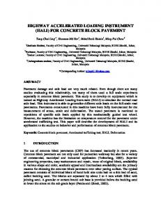
Figure 1. Programmability spectrum of cell and routing fabric. by a flip-flop. Since flip-flops are not used as frequently as LUTs, the utilization of transistors in VCLBs is low. The second type of VCLB is based on PLA structure [16]. PLA enables implementation of two-level logic functions, but it still needs flip-flops for implementing a sequential design. The third type of VCLBs [7] uses series-parallel layout structures to implement either combinational logic gates or flip-flops. Since our work is closely related to this type of VCLB, we will detail the work proposed in [7]. Two viaconfigurable base-cells are proposed in [7]. One is called nViaCC (or n-VCC for short) that consists of n pairs of P-N transistors. These transistors can be configured to implement n or fewer input functions. A 5-VCC in Fig. 2 is specially proposed. One can refer [7] to see which logic functions can be realized by a 5-VCC. A via in a 5-VCC can be installed at the place where an M1 line and an M2 line intersect. All the layers below M1 are pre-fabricated and M2 layer is with predefined mask patterns. Only the M1-M2 vias can be used to set the logic functions of a 5-VCC. The M2 P/G lines run horizontally in parallel with diffusions and M1 wires run vertically in orthogonal to M2 wires. The other base-cell is called inverter array(INVA for short) which can be used to implement inverters, XOR/XNORs, multiplexers, etc. An INVA has three diffusion strips for each type of transistors. A layout of INVA is shown in Fig. 2 where P/G lines are run horizontally in M1. A 5-VCC and an INVA can be combined to implement a flip-flop. An even larger programmable block called VCGA as shown in Fig. 3 is also presented. A VCGA has four basic logic elements (BLE). Each BLE has a 5-VCC and two INVAs. Note that an INVA takes a larger area than a 5-VCC. There are some problems with this VCGA. z The short P/G lines in a VCGA are laid out on two different layers. Connecting them together, we must use a large number of vias and M1/M2 wires. This drastically increases the resistance of P/G network. Moreover, we need to add extra vias to connect the P/G networks among VCGAs, this further increases the P/G network resistance. Note that the P/G lines in a VCC and an INVA are not located at the boundaries so that row abutting to make wider P/G lines is not possible. z We need to implement a complicate P/G network using higher metal layers (M3 or above) no matter whether the P/G lines in VCCs and INVAs are configured to be connected or not. Moreover, we can not freely drop a via from an M3 P/G strap to an M1 P/G line because a short to M2 signal wires in INVAs may occur. z The number of functions that can be implemented by a VCGA is large and some of them can be very complex. Creating a library that consists of these functions for logic synthesis, physical design, and timing analysis tools is very difficult. No discussion of such efforts is made in [7]. In summary, the above drawbacks prevent VCGAs from being used as standard cells. Yet another problem with VCGA is that the fourth quadrant of a BLE does not have any transistors. Our standard cell like VCLB does not have the aforementioned problems.
Table 1. Programmability choices. Vendors/ Researchers LSI
Grain size Fine
Programmability
Cell
Metal SRAMeASIC Coarse based LUT Virage Logic Fine Metal NEC Coarse Metal AMI ? Metal ChipX ? Metal Fujitsu ? Metal Faraday ? Metal Altera Fine Metal ViASIC Coarse Via Triad Semi. ? Via Synopsys [5] Coarse Via Marek- Sadowska et al. Coarse Via Pilleggi et al. Coarse Via Ours Medium Via
Unified Routing fabric c&s? Metal ? Via
No
Metal Metal Metal Metal Metal Metal Metal Via Via Via Via Metal/Via Metal
? No ? ? ? ? Yes No ? No Yes No Yes
In this paper, we propose a medium grained viaprogrammable CLB (VCLB). Our VCLBs along with either a metal or a via-programmable routing fabric can be used to construct a structured ASIC. Each VCLB has five pairs of PN transistors. These transistors can be configured into a logic function with five or fewer inputs using M1-M2 vias. VCLBs can be abutted to form a more complex function using the jumpers at their both ends. The same VCLB can be used to implement either combinational or sequential elements. Power/ground (P/G) buses are placed on M2 to facilitate the deployment of M3 power straps. They are located at the top and bottom boundaries so that they can be made wider by cell row abutment. We establish a design flow primarily using commercial standard cell design tools. Our own tools include a logic packer and a placement legalizer. We create a 0.18um standard cell library based on our VCLB to test our design flow and to evaluate the viability of our VCLB. Experimental results show that our structured ASIC fabric with programmable metals for routing achieves a delay of 2.7 times, an area of 3 times, and a power of 1.5 times that attained by the designs using a commercial standard cell library. The method we propose here to evaluate the viability of a structured ASIC fabric is very important. It is based on the concept of pushing the delay envelope to see how small a delay can be achieved using a programmable fabric. The rest of this paper is organized as follows. Section 2 discusses some VCLB design problems. Section 3 presents our programmable fabric. Section 4 describes our design methodology. Section 5 presents some experimental results. The last section draws conclusions and discusses future work.
2. Existing VCLBs
There are three types of VCLB. First, a VCLB can be an FPGA-like look-up table (LUT). LUT-based VCLBs proposed in [4] can be laid out in a way similar to standard cells. Standard cell design style enables simple P/G distribution. P/G buses between adjacent cells can be abutted and P/G straps using higher metal layers can be easily deployed to form a P/G network. The major problem of LUT-based VCLBs is that each LUT must be accompanied
382
does not have a chance to create a short circuit from power to ground. However, a choice of connecting a pin to P/G can always be made. z A VCLB has five long M2 wires for intra VCLB connections and three M1 jumpers at both ends for inter VCLB connections. The jumpers enable the composition of our VCLBs so that a more complex logic function can be implemented using several VCLBs. z Creating a cell library using our VCLB is considerably easier than that using VCGA given in Fig. 3 because the number of logic functions that can be implemented by our VCLB is much smaller. Our VCLB with respect to power planning is similar to that presented in [5]. However, there are two important differences. One is that each CLB in [5] must contain a fixed ratio of combinational logic elements to sequential elements. The other is that the CLB in [5] lacks composition capability.
Figure 2. Layouts of 5-VCC (top) and INVA.
Figure 3. A VCGA proposed in [7].
3. Proposed programmable fabric
Our programmable fabric has a two dimensional array of VCLBs and a metal programmable routing fabric. We will first describe our VCLB and then demonstrate the configurability and composition capability of our VCLBs.
3.1. Layout of our VCLB
Fig. 4 shows the stick diagram and layout of our VCLB. Our VCLB has five transistor pairs. The three transistor pairs on the left are used to form CMOS logic and the two transistor pairs on the right are used to form pass transistor logic. CMOS logic is implemented using serial-parallel structures. Pass transistors can be better used to implement multiplexers and XOR/XNOR. Vias can be selectively inserted at the junctions of M1 and M2 wires to implement a logic function. Almost all the logic functions realized by a 5VCC can be implemented by our VCLB. Despite of a resemblance between our VCLB and the 5VCC and INVA, our VCLB has the following features. z Our VCLB is a monolithic block. It is asymmetric and can not be flipped w. r. t. Y-axis for structured ASIC designs. z The preferable routing directions of M1 and M2 are vertical and horizontal, respectively. z M2 P/G lines are located at the top and bottom boundaries. Our VCLBs can be abutted seamlessly to form a cell row. A cell row can be flipped w. r. t. X-axis so that it can abut the rows above and below it to form wider P/G lines. z M3 (or high layer) P/G straps can be freely deployed above the core area because they can be connected to the M2 P/G lines in the cells without any restriction. Basically, what can be done for a traditional standard cell design can also be done for a design based on our VCLBs. z The I/O pins are the short vertical M2 wire segments located at the central strap of the VCLB. They are on-grid and have enough space for via doubling. The unused inputs need not be tied to P/G because any floating input
Figure 4. Proposed VCLB.
3.2. Configurability and composition capability
Here, we will show the configurability and composition capability of our VCLBs. The layout in Fig. 5 (left) is a 2-to1 multiplexer. The third pair of P-N transistors is used to create the complement of S0 and the two pairs of P-N transistors on the right are used to form two transmission gates. Two pairs of transistors are unused. Fig. 5 (center) shows a layout for AOI221X4. The layout consists of two VCLBs. A buffer of 4X driving capability is implemented in one VCLB. Fig. 5 (right) shows a layout of a positive edge triggered D flip-flop with active low reset. The layout consists of three VCLBs. From the above two layouts, one may find that the jumpers between two VCLBs have been employed to send signals from one VCLB to another. Note that more complex functions can be realized using a various number of VCLBs. Large drive inverters and buffers can be realized in a similar way. The VCLB can be modified to provide more jumpers and long wires for inter cell connections. Our library will have logic functions that uses two or more VCLBs. A multi-VCLB logic block can be freely placed at any legal position as long as it is confined within a cell row. That is to say, it is relocatable. Besides, more than one basic logic function can be packed into the same VCLB. Later, we will present a logic packer that carries out the packing task for a synthesized design.
383
Figure 5. Layout of 2-to-1 multiplexer (left), layout of AOI221X4 (center), and layout of a D flip-flop. Step 1: A graph is created. A non-fully used VCLB is modeled as a vertex. An edge between two vertices is created if the two corresponding VCLBs can be combined into one VCLB. Any two VCLBs can be combined into one VCLB if there is a corresponding MFPB in the SOC-E cell library. Each edge is assigned a weight using the approach proposed in [18]. The edge weight represents how strongly the two related VCLBs should be connected. Step 2: We first perform a maximum weight bipartite matching on a subgraph formed by VCLBs, each of which implements either a 4-input or 1-input basic logic function. Once this is done, any two matched VCLBs are combined into one VCLB and the two vertices corresponding to the two original VCLBs are removed from the graph. Any 4-input VCLB that can not find a matching should be removed from the original graph. This step is repeated for a subgraph comprised of 3-input and 2-input VCLBs and a subgraph comprised of 3-input and 1-input VCLBs. Step 3: We perform a general maximum weight matching on a subgraph comprised of only 2-input VCLBs, 2-input and 1-input VCLBs, and only 1-input VCLBs, respectively. Fig. 7 shows a logic packing example. Fig. 7(a) is the original graph. Fig. 7(b) is the matchings for the subgraph comprised of 3-input VCLBs and 2-input VCLBs. The graph in Fig. 7(c) is obtained by deleting the vertices with matchings and the un-matched vertices that correspond to 3input VCLBs. The matchings in Fig. 7(c) are for 2-input VCLBs only. We obtain an optimal solution for the example in terms of the number of matchings and total edge weights.
4. Design methodology
Here, we present a design methodology for structured ASICs. Fig. 6 shows a simple flow of how to construct a standard cell library (the shaded part) and perform chip designs using a cell library based on our VCLB. To create a cell library, we first define a via map for each logic function. We install the so-defined vias on a VCLB to complete the layout of a logic function. We use Mentor’s Calibre to extract post-layout parasitics and the tool in [17] to perform post layout timing characterization. Once this is done, we create a library called DC cell library for Synopsys Design Compiler. In DC cell library, since the transistors in the VCLBs for simple logic functions are not fully utilized, we hand-pack two logic functions into a single VCLB to form a multifunction packed block (MFPB). Determining which basic logic functions should be put into an MFPB is very complicate. We only combine the most frequently used logic functions into one MFPB. Accordingly, we have to create a layout for each MFPB. Once this is done, we create a library called SOC-E cell library for Cadence SOC Encounter. SOCE cell library has packed versus non-packed logic blocks. A design flow mostly using commercial tools such as logic synthesizer, placer, router, timing analyzer, etc. is also shown in Fig. 6. The tools developed by ourselves are a logic packer and a placement legalizer.
4.1. Logic packer
Our logic packer places two logic functions into a VCLB. It has the following steps.
4.2. Placement legalizer
Our placement legalizer takes the result from a standard cell placer as input and determines a legal position for each cell such that the total displacement of all cells from their original positions is minimized. We assume that the order of the cells in a cell row is preserved. The legalizer is run for the cells in each row. A legal position for a cell in a row should be an integral multiple of VCLB width. This problem is formulated as a minimum weight bipartite matching problem. We create a bipartite graph as follows. A cell is modeled as a vertex in one group. The vertices in this group is denoted as Ci, i=0, n-1. Each of the legal positions on a row is modeled as a vertex in the other group. The vertices in this group is denoted as Rj, j=0, m-1. An edge between Ci and Rj is created if Rj is a permissible position for vertex Ci. A permissible position for Ci is a legal position so that there is at least a placement solution for all the cells in a row if Ci is placed at that position. Let the width of Ci be wi, the total width of the cells to the left of Ci be A i , the total width of all the cells to the right of Ci be A i ' , and the length of a row be A r , all in terms of the VCLB width. Then, the permissible position for Ci starts from A i and terminates at A r − (A i ' + wi ) . A weight is assigned to each edge between Ci and its permissible position Rj. The weight is set to the distance between the original position of Ci and Rj. Fig. 8(a) shows a cell row with
Figure 6. Library and chip design methodology.
Figure 7. An example of logic packing.
384
For example, the total area of b14 using STDL corresponding to the case with the smallest longest path delay is 283000 um2 and it is 679000 um2 for the case using YZUL. Thus, we have an area ratio of 2.4. Power ratio is similarly calculated. The power ratios of some circuits are smaller than 1. This does not mean that the circuits using YZUL consume less power because the circuits using YZUL have their delays several times more than that of the circuits using STDL. If we push the delay envelope, the delay of our structured ASIC designs is on average 2.7 times that of their standard cell counterparts at the expense of 3 times area and 1.5 times power. These data serve as achievable lower bounds for the case of using a via-programmable routing fabric. The last two columns in Table 8 present some interesting data about achievable delay envelope. A value in the last column is the ratio of the largest longest path delay of a circuit using YZUL to the smallest longest path delay of the same circuit also using YZUL. A value in the column “STDL max/min delay ratio” is calculated similarly. We find that the circuits using STDL have much larger ratios. This implies that a standard cell library can enable more aggressive delay optimization than our YZUL. This is an important observation which gives a clear direction for the future research on CLBs. Part of the reason why YZUL achieves a smaller ratio is that each cell in YZUL has much more parasitic capacitance than that in STDL and thus has a larger cell delay. As a result, the total cell delay takes a dominant part of critical path delay of a circuit using YZUL so that its critical path can not be effectively optimized. Transistor utilization of the VCLBs in the circuits using YZUL is on average 73%. This is smaller than that reported in [7]. Part of the reason for this is that we do not pack the un-related VCLBs. Making a comparison of our results to the previous works [5,7] is difficult because they do not perform experiments like ours, i.e., not performing experiments to push delay envelope. The comparison depends on which point on the delay curve is used, whether layout parasitics are considered, what kinds of tools are used, etc. However, if a comparison must be made, our YZUL on average achieves a delay-area product of 8.0 and a delay-power product of 3.9 whereas the work in [5] from an EDA company on average achieves a delay-area product of 14.8 and a delay-power product of 5.4. Note that the work in [5] has a via-programmable routing fabric rather than a metal programmable routing fabric like ours. The work in [7], having a metal programmable routing fabric, achieves a delay-area product of 2.87 and a powerdelay product of 1.56. However, these data are obtained without performing detailed routing.
cells C0 and C1 whose positions are originally at 7.25 and 21. The width of a VCLB is 10. The permissible positions are 0, 10, 20 for C0 and 10, 20, 30 for C1, respectively. Fig. 8(c) shows a minimum weight bipartite matching which places C0 at 10 and C1 at 20, with a minimum weight of 3.75.
Figure 8. An example of legalizing cell positions.
5. Experimental results
We have implemented a cell library using our VCLB for evaluating the design methodology described in Fig. 6. When implemented using 0.18um process technology, our VCLB has an area of 78 um2. The library consists of 105 unpacked cells and 73 packed cells. We selectively implement some functions that are found frequently used by a logic synthesis tool. Most of the logic functions except inverter, buffer, and flip-flop have driving capability of 1X, 2X, 4X. Buffer has driving capability from 1X up to 16X and inverter has driving capability from 1X up to 20X. D flip-flop with reset has driving capability of 1X and 2X. Power and timing data of each cell are characterized using HSPICE. Two kinds of experiments are performed. One uses our library (YZUL for short) for doing chip design. The other uses a commercial standard cell library (STDL for short). Both libraries are based on the same 0.18um process technology. The same parameter settings such as power ring width, core utilization, etc. are used to design chips regardless of which library is used. The designs using YZUL are routed without using M1 and M2 layers whereas those using STDL are routed with M1 and M2 layers. The large benchmark circuits from ISCAS89 and ITC99 are used in our experiments. Our experiments are carried out in the following manner. First, we use Synopsys Design Compiler to synthesize each circuit without any timing requirements but aiming only to minimize the area. We then find the longest path delay for each circuit after the circuit is routed. We call such a delay base_delay. We then perform logic synthesis for each circuit with clock period specified as 0.9*base_delay, 0.8*base_delay, 0.65*base_delay, 0.5*base_delay, 0.35*base_delay, 0.2*based_delay, and 0.1*based_delay, respecyively. The reason for carrying out experiments in this way is to see how far we can push the delay envelope of the designs using each library. Tables 2 and 3 show the longest path delays of the postrouted circuits respectively designed with both libraries. The numbers of cells and nets of the circuits synthesized without timing requirements using STDL are also given in Table 2. The columns denoted by “1” give the base_delays. The columns denoted by “0.9” give the longest path delay for the cases with clock period specified as 0.9*base_delay. Tables 4 and 5 show the cell areas of the designs. Tables 6 and 7 present the total power dissipation. Table 8 summarizes the delay, area, and power data. The column “Delay ratio” gives the ratio of the smallest longest path delay of a circuit using YZUL to that of the same circuit using STDL. For example, the small longest path delay of b14 using STDL is 4.9ns and it is 10.5ns for the case using YZUL. Thus, we have a ratio of 2.1. The area and power ratios are calculated accordingly.
Table 2. Longest path delay of designs using STDL (ns). s35932 s38417 s38584 b14 b15 b17 b18 b19 b20 b21 b22 Ave
*
Cells 3929 5033 6067 2217 3127 10290 28002 58545 4674 4561 6894
Nets 4553 5189 6474 2666 3448 10509 30647 60412 5389 5263 7966
1 11.2 4.9 36.7 19.7 35.3 28.7 29.2 36.6 19.8 20.0 21.0 23.9
0.9 12.3 3.5 4.7 14.3 14.6 12.8 17.7 20.0 15.3 15.0 17.2 13.4
0.8 13.0 3.4 5.0 13.9 12.9 12.7 16.9 18.1 14.9 15.7 17.4 13.1
0.65 11.4 3.2 5.0 11.4 14.6 13.4 15.3 16.5 12.4 12.1 16.0 12.0
0.5 12.4 2.9 5.4 6.8 12.2 11.6 15.0 16.0 7.0 7.6 10.3 9.7
0.35 9.4 2.8 4.9 6.5 10.1 16.0 10.3 13.6 9.8 7.0 9.0 9.0
0.2 13.2 2.8 3.9 4.9 8.3 19.1 8.6 17.2 6.1 5.4 5.3 8.6
0.1 2.0* 2.7 3.1 5.6 13.0 14.3 13.2 13.6 5.8 5.5 6.3 7.7
This is not an error. This delay value is achieved due to having proper fanout optimization.
385
Table 7. Power dissipation of the designs using YZUL (mw, at 100MHZ, 20% toggling rate).
6. Conclusions and future work
In this paper, we have proposed a standard cell like VCLB such that existing tools for standard cell designs can be leveraged to design a structured ASIC based on our VCLB. Our approach achieves a delay of 2.7 times, an area of 3 times, and a power of 1.5 times that attained by the designs using a commercial standard cell library if we push the delay envelope of the designs. Currently, we are working on a via-programmable routing fabric and developing a router for it. A clock tree synthesizer and some timing and power optimization methods are yet to be developed.
s35932 s38417 s38584 b14 b15 b17 b18 b19 b20 b21 b22 Ave
Table 3. Longest path delay of designs using YZUL (ns). s35932 s38417 s38584 b14 b15 b17 b18 b19 b20 b21 b22 Ave
1 31.7 8.0 21.1 21.6 66.9 44.7 53.7 55.4 22.2 28.3 31.9 35.0
0.9 0.8 0.65 25.8 35.8 22.2 7.3 7.7 6.8 8.3 7.1 8.8 16.0 13.6 13.4 20.6 20.7 20.5 19.6 21.0 18.7 24.8 29.2 28.0 27.1 31.4 30.9 15.6 15.8 17.2 23.4 15.3 15.4 30.3 23.4 21.3 19.9 20.1 18.5
0.5 0.35 0.2 32.8 21.7 32.6 6.3 6.5 6.3 7.5 6.6 5.8 10.5 11.1 11.6 19.2 16.5 13.2 17.7 15.5 17.0 28.1 26.0 36.7 28.2 20.9 22.1 17.0 21.1 20.2 16.0 16.4 19.1 24.1 26.7 31.9 18.8 17.2 19.7
0.1 11.4 6.9 6.7 12.4 14.4 16.2 37.6 29.4 18.9 17.5 30.7 18.4
0.9 182 196 169 123 121 360 996 1938 244 237 343 446
0.8 0.65 182 182 205 232 169 169 143 169 122 121 360 360 1003 1007 1944 1970 291 353 268 439 363 473 459 498
0.5 0.35 182 182 273 293 169 169 102 130 121 128 368 415 1099 1079 1996 2350 214 331 209 316 322 438 459 530
0.2 191 309 170 283 166 522 1595 2640 535 566 810 708
0.1 268 308 183 276 206 634 1694 3022 560 595 803 777
0.9 787 780 699 468 493 1466 4032 8024 996 1413 1746 1900
0.8 787 809 698 499 492 1467 4077 8104 989 929 1772 1875
0.65 787 915 698 549 493 1474 4152 8251 1291 993 1502 1919
0.5 787 1038 701 679 493 1488 4341 8655 1594 1366 1815 2087
0.35 787 1094 713 871 493 1712 4456 8659 1927 1911 2488 2283
0.2 788 1153 812 1044 596 2102 5801 11210 2040 2012 2917 2771
0.10 820 1115 915 951 762 2189 6089 11905 1989 2049 2935 2884
Table 6. Power dissipation of the designs using STDL (mw, at 100MHZ, 20% toggling rate). s35932 s38417 s38584 b14 b15 b17 b18 b19 b20 b21 b22 Ave
1 3.6 5.6 5.1 2.9 3.7 12.6 32.6 70.0 5.9 5.8 8.7 14.2
0.9 3.3 6.0 5.5 4.1 3.8 12.8 36.9 73.1 8.7 8.1 11.8 15.8
0.8 0.65 3.4 3.4 6.5 7.6 5.5 5.5 5.0 5.8 3.8 3.8 12.8 12.8 36.9 36.9 73.1 74.3 10.8 12.5 9.6 12.7 13.3 17.9 16.4 17.6
0.5 0.35 3.3 3.4 9.2 9.9 5.5 5.4 3.5 4.6 3.8 4.0 13.0 14.2 39.7 38.8 74.4 82.6 7.6 12.8 7.4 12.1 12.1 16.9 16.3 18.6
0.2 3.4 10.8 5.6 12.2 5.3 19.9 61.5 98.3 22.9 24.4 33.9 27.1
0.2 17.4 19.3 17.1 15.2 10.2 35.7 96.9 188.5 29.6 29.0 42.8 45.6
0.1 19.6 19.6 17.9 13.8 11.7 35.1 96.7 193.0 28.8 29.4 44.5 46.4
[1] HardCopy Structured ASICs: ASIC gain without the pain. http://www.altera. com/products/software/flows/asic/qts-structured_asic.html [2] B. Zahiri, “Structured ASICs: opportunities and challenges,” ICCD, 2003, pp. 404-409. [3] K. C. Wu, Y. W. Tsai, “structured ASIC, evolution or revolution?” ISPD, pp.103-106, 2004. [4] L. Pileggi et al., “Exploring regular fabrics to optimize the performancecost trade-off,” DAC, 2004, 782-787. [5] N. V. Shenoy, J. Kawa, R. Camposano, “Design automation for mask programmable fabrics,” DAC, 2004, pp. 192-197. [6] C. Patel, A. Cozzie, H. Schmit, and L. Pileggi, “An architectural exploration of via patterned gate arrays,” ISPD, 2003, pp. 184–189 [7] Y. Ran and M. Marek-Sadowska, "Designing via-configurable logic blocks for regular fabric", IEEE Trans. on VLSI Systems, Vol. 14, No. 1, Jan. 2006. [8] A. Koorapaty, L. Pileggi, and H. Schmit, “Heterogeneous logic block architectures for via-patterned programmable fabrics,” LNCS 2778, 2003, pp. 426–436. [9] Y. Ran and M. Marek-Sadowska, “Via-configurable routing architectures and fast design mappability estimation for regular fabrics,” IEEE Trans. on VLSI Systems, Vol. 14, Sept. 2006, pp. 998-1009. [10] A. Levinthal and R. Herveille, “FlexASIC structured array: a solution to the DSM challenge,” DesignCon 2005. [11] V. Kheterpal, et al., “Design methodology for IC manufacturability based on regular logic-bricks,” DAC, 2005, pp.192-197. [12] D. D. Sherlekar, “Design considerations for regular fabrics,” ISPD, April 18-21,2004, pp.97-102. [13] A. Koorapaty, et al. “Exploring logic block granularity for regular fabrics,” DATE, 2004, pp. 1468-473. [14] White paper, “RapidChip technology: fast custom silicon through platform-based design,” LSI Logic, 2004. [15] T. Okamoto, T. Kimoto, N. Maeda, “Design methodology and tools for NEC electronics’ structured ASIC ISSP,” ISPD, 2004, pp.90-96. [16] F. Mo, R. Brayton, “PLA-based regular structures and their synthesis,” IEEE Trans. on TCAD, Vol. 22, No. 6, June 2003, pp.723 - 729. [17] Shu-Ren Ker, “An Automatic Library Development System,” Master Thesis, Yuan Ze University, Taiwan, June 1997. [18] B. Hu and M. Marek-Sadowska, “Wire length prediction based clustering and its application in placement,” DAC, 2003, pp. 800-805.
2
1 783 715 706 274 434 1237 3236 6336 544 531 801 1418
0.5 0.35 17.5 17.8 18.0 18.5 15.7 15.9 10.0 12.7 8.9 9.3 28.5 31.8 80.9 79.5 161.5 156.8 23.9 27.0 20.8 27.8 28.3 38.1 37.6 39.6
7. References
Table 5. Total cell area of designs using YZUL (x1000um ). s35932 s38417 s38584 b14 b15 b17 b18 b19 b20 b21 b22 Ave
0.8 0.65 17.4 17.5 15.7 16.7 15.9 15.7 7.3 8.4 9.0 8.8 28.2 29.1 78.1 79.1 157.6 158.6 15.1 19.5 14.2 15.0 26.6 23.5 35.0 35.6
Table 8. Delay, area, and power ratio
2
1 180 180 173 88 116 337 953 1880 170 166 248 408
0.9 17.4 15.5 15.8 6.7 9.0 28.4 76.9 154.3 15.3 21.3 27.6 35.3
Delay Delay STDL YZUL Delay Area Power *powe * max/min max/min ratio ratio ratio r area delay ratio delay ratio s35932 5.8 3.1 2.1 12.2 17.9 6.8 2.8 s38417 2.4 3.7 1.8 4.2 8.8 1.8 1.3 s38584 1.9 4.4 2.8 5.2 8.2 11.9 3.7 b14 2.1 2.4 0.8 1.8 5.2 4.0 2.0 b15 1.6 3.6 1.9 3.1 5.7 4.2 5.1 b17 1.3 4.6 2.4 3.3 6.2 2.5 2.9 b18 2.9 2.5 1.3 3.6 7.3 3.4 2.2 b19 1.5 3.7 1.9 2.9 5.7 2.7 2.6 b20 2.7 1.8 0.6 1.7 4.8 3.4 1.4 b21 2.8 1.6 0.6 1.7 4.7 3.7 1.8 b22 4.0 1.9 0.7 2.8 7.5 4.0 1.5 2.7 3.0 1.5 3.9 8.0 4.4 2.5 Ave
Table 4. Total cell area of designs using STDL (x1000um ). s35932 s38417 s38584 b14 b15 b17 b18 b19 b20 b21 b22 Ave
1.0 15.8 15.7 14.6 4.8 8.3 25.1 65.8 128.1 9.9 9.5 14.9 28.4
0.1 9.4 10.8 6.2 11.9 7.6 25.3 66.3 118.8 24.8 26.7 36.0 31.3
386