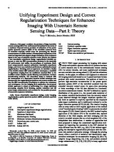
Article
Study and Experiment on Non-Contact Voltage Sensor Suitable for Three-Phase Transmission Line Qiang Zhou 1, *, Wei He 1 , Dongping Xiao 1 , Songnong Li 2 and Kongjun Zhou 2 Received: 21 November 2015; Accepted: 25 December 2015; Published: 30 December 2015 Academic Editor: Vittorio M. N. Passaro 1
2
*
State Key Laboratory of Power Transmission Equipment & System Security and New Technology, Chongqing University, Chongqing 400044, China;
[email protected] (W.H.);
[email protected] (D.X.) State Grid Chongqing Electric Power CO. Electric Power Research Institute, Chongqing 400015, China;
[email protected] (S.L.);
[email protected] (K.Z.) Correspondence:
[email protected]; Tel.: +86-132-7192-0913
Abstract: A voltage transformer, as voltage signal detection equipment, plays an important role in a power system. Presently, more and more electric power systems are adopting potential transformer and capacitance voltage transformers. Transformers are often large in volume and heavyweight, their insulation design is difficult, and an iron core or multi-grade capacitance voltage division structure is generally adopted. As a result, the detection accuracy of transformer is reduced, a huge phase difference exists between detection signal and voltage signal to be measured, and the detection signal cannot accurately and timely reflect the change of conductor voltage signal to be measured. By aiming at the current problems of electric transformation, based on electrostatic induction principle, this paper designed a non-contact voltage sensor and gained detection signal of the sensor through electrostatic coupling for the electric field generated by electric charges of the conductor to be measured. The insulation structure design of the sensor is simple and its volume is small; phase difference of sensor measurement is effectively reduced through optimization design of the electrode; and voltage division ratio and measurement accuracy are increased. The voltage sensor was tested on the experimental platform of simulating three-phase transmission line. According to the result, the designed non-contact voltage sensor can realize accurate and real-time measurement for the conductor voltage. It can be applied to online monitoring for the voltage of three-phase transmission line or three-phase distribution network line, which is in accordance with the development direction of the smart grid. Keywords: voltage sensor; non-contact measurement; ansoft maxwell; electric field intensity; three phase transmission lines
1. Introduction The voltage transformer is an important part of an electric power system and the detection performance of the transformer can directly influence the reliability of an electric power system voltage measurement and relay protection device motion as well as the accuracy of electric power measurement. Presently, voltage transformers extensively applied to electric power system mainly include potential transformer and capacitance voltage transformer [1–5]. Structure diagram of Capacitance Voltage Transformer (CVT) is shown in Figure 1. The high voltage terminal is directly connected to electrified body and the other terminal is connected to the ground; C1 and C2 are adopted for capacitance voltage division, and voltage signal after voltage division will be transformed into output signal of transformer through potential transformer [6–9].
Sensors 2016, 16, 40; doi:10.3390/s16010040
www.mdpi.com/journal/sensors
Sensors 2016, 16, 40
2 of 21
Sensors 2016, 16, 40 Sensors 2016, 16, 40
Figure 1. Structure diagram of CVT.
Figure 1. Structure diagram of CVT. Figure 1. Structure diagram of CVT.
Potential transformer is shown in Figure 2, and the high voltage terminal is connected to Potential transformer is is shown the high highvoltage voltageterminal terminal is connected electrified body. Potential transformer shownininFigure Figure 2, 2, and and the is connected to to electrified body.body. electrified U 1 2 U 1 3 2 3
N N
1:primary winding 4 2:balanced winding 1:primary winding 5 4 3: iron core winding 2:balanced 5 4-5:signal output 3: iron core 4-5:signal output
Figure 2. Potential transformer.
Figure 2. Potential transformer.
Figure 12. and Potential transformer. According to analysis the Figures 2, the traditional voltage transformers shown in Figures 1 and 2, the high voltage currently voltage transformer has direct shown electrical According to analysis the terminal Figures 1of and 2, theused traditional voltage transformers in According to2,analysis the Figures 1 of and 2thethe traditional voltage transformers shown in connection with conductor to be measured, and other terminal the transformer is connected Figures 1 and the high voltage terminal currently used voltage of transformer has direct electrical to the ground. Therefore, insulation design of the the other transformer isoftransformer difficult, and,has meanwhile, it connection withhigh conductor to terminal be measured, and the transformer is connected Figures 1 and 2 the voltage of currently usedterminal voltage direct electrical involves a large volume and heavyweight; due to the iron core design and multi-grade capacitance to the ground. Therefore, insulation design of the transformer is difficult, and, meanwhile, it to connection with conductor to be measured, and the other terminal of the transformer is connected voltage division of the transformer, serious time delays occur during the detection signal and involves a large volume and heavyweight; due to the iron core design and multi-grade capacitance the ground. Therefore, insulation design of the transformer is difficult, and, meanwhile, it involves voltage signal to beofmeasured in phase serious position.time As adelays result, detection accuracy of the transformer is voltage division the transformer, occur during the detection signal and a large volume and heavyweight; due to the iron core design and multi-grade capacitance voltage reduced and its application range is restricted. Moreover, three-phase voltage transformer is voltage signal to be measured in phase position. As a result, detection accuracy of the transformer is division of the transformer, serious time delays occur during the detection signal and voltage signal to seldom the voltagerange grade is above 35 kV in electric power systems.voltage Therefore, traditionalis reducedadopted and itsforapplication restricted. Moreover, three-phase transformer be measured in phase position. As a satisfy result,the detection accuracy ofelectric the transformer is reduced and its voltage transformers can no longer development of the power system [10–12]. seldom adopted for the voltage grade above 35 kV in electric power systems. Therefore, traditional application range is restricted. Moreover, three-phase voltage transformer isa seldom for the In consideration of thisofpaper designed non-contact voltage voltage transformers canthe noabove-mentioned longer satisfy the problems, development the electric power systemadopted [10–12]. voltage grade above 35 kV in electric power systems. Therefore, traditional voltage transformers sensor on the basis of electric field coupling principle, as shown in Figure 3. In Figures 1–3 are In consideration of the above-mentioned problems, this paper designed a non-contact voltage can no longer satisfy the development of the electric power system [10–12]. non-contact voltage sensors installed on the three-phase transmission line. Positive and negative sensor on the basis of electric field coupling principle, as shown in Figure 3. In Figures 1–3 are induction electrodes on the and the electric field designed produced by electric charges non-contact voltage sensors installed onsensor, the problems, three-phase transmission line. Positive and negative In consideration ofare thedesigned above-mentioned this paper a non-contact voltage on the the transmission generate induced charges on as theshown electrode ofFigure voltage3. sensor by charges way 1–3 of are induction electrodes arewill designed the sensor, and the electric fieldinproduced by electric sensor on basis of line electric field on coupling principle, In Figures electrostatic induction. The electric charges will distribute on the electrode to form electric potential, on the transmission line will generate induced charges on the electrode of voltage sensor by way of non-contact voltage sensors installed on the three-phase transmission line. Positive and negative and the potential signal ofelectric positive and negative induction electrodes is form output signal of the electrostatic induction. The charges will distribute on the electrode to electric potential, induction electrodes are designed on the sensor, and the electric field produced by electric charges non-contact voltage signal sensor.of positive and negative induction electrodes is output signal of the and the potential on the transmission line will generate induced charges on the electrode of voltage sensor by way of Compared withsensor. traditional voltage transformer, non-contact voltage sensor has no electrical non-contact voltage electrostatic induction. The electric charges will on the is electrode to form electric connection with electrified body. Therefore, thedistribute insulation design simple and thehas cost is electrical low;potential, the Compared with traditional voltage transformer, non-contact voltage sensor no and the potential signal of positive and negative induction electrodes is output signal of the non-contact induction of non-contact voltage the sensor is optimized connectionelectrode with electrified body. Therefore, insulation design through is simple simulation and the costcalculation. is low; the voltage sensor.design Miniature of the is realized, the sensor voltageisdivision ratio through is increased, and phase error of induction electrode of sensor non-contact voltage optimized simulation calculation. sensor detection reduced. An experimental that of aand 50 kV Compared withsignal traditional voltage transformer, non-contact sensor hassimulated no electrical Miniature design of theissensor is realized, the voltageplatform division ratioconsisted isvoltage increased, phase error of three-phase transmission line was established theplatform laboratory test the of non-contact voltage sensor with detection signal isbody. reduced. An experimental thattoconsisted a and 50 kV simulated connection electrified Therefore, thein insulation design is simple the cost is low; sensor designed in this paper. According to the the designed voltage sensor can calculation. realize three-phase transmission line was established inresult, theislaboratory to through test the non-contact voltage the induction electrode of non-contact voltage sensor optimized simulation real-time detection for the voltage of three-phase transmission line and accurately measure the sensor designed in this paper. According to the result, the designed voltage sensor can realize Miniature design of the sensor is realized, the voltage division ratio is increased, and phase error of voltage and phase position. real-time detection for the voltage of three-phase transmission line and accurately measure the sensor detection signal is reduced. An experimental platform that consisted of a 50 kV simulated voltage and phase position.
three-phase transmission line was established in the laboratory to test the non-contact voltage sensor designed in this paper. According to the result, 2the designed voltage sensor can realize real-time 2 detection for the voltage of three-phase transmission line and accurately measure the voltage and phase position.
Sensors 2016, 16, 40
3 of 21
Sensors 2016, 16, 40
Sensors 2016, 16, 40
Figure 3. Application of voltage sensor in transmission line.
Figure 3. Application of voltage sensor in transmission line.
Non-contact voltage sensor used at the laboratory test stage adopts closed annular electrode, 3. Application of voltage sensor in transmission line. test of the sensor. In and it is mainly appliedFigure to detection and insulation performance Non-contact voltage sensor used performance at the laboratory test stage adopts closed annular electrode, the follow-up study, open-type annular electrode presented in Figure 4 will be designed. and it is mainly applied to detection performance and insulation performance testThe of sensor the sensor. Non-contact voltage sensor used at the laboratory test stage adopts closed annular electrode, can be conveniently installed on the line, while the signal detection and processing circuit and In theand follow-up study, open-type annular electrode presented in Figure 4 will be designed. The sensor it is mainly applied to detection performance and insulation performance test of the sensor. In wireless transmission circuit will be designed. In this way, the detection signal can be transferred to can be conveniently installed on the line, while the signal detection and processing circuit and wireless the follow-up study, open-type annular electrode presented in Figure 4 will be designed. The sensor the control terminal in time. In Figure 4, 1 refers to non-contact voltage sensor; 2 is the insulation transmission circuit will be designed. In this signal can transferred to theand control can be conveniently installed on the line,way, whilethe thedetection signal detection andbeprocessing circuit fixture—rubber with good insulation performance and toughness is used in the center fixture so wireless transmission circuit will betodesigned. In this way, the detection signal can be transferred to terminal in time. In Figure 4, 1 refers non-contact voltage sensor; 2 is the insulation fixture—rubber that when the fixture is compressed, the centers of the line and sensor electrode can be maintained the control terminal in time. In Figure 4, 1 refersistoused non-contact voltage sensor; 2that is the insulation with in good insulation performance and toughness in the center fixture so when the fixture the coaxial position, owing to the existence of non-conducting rubber; 3 indicates the signal fixture—rubber with good insulation performance and toughness is used in the center fixture so is compressed, the centers of the line and sensor can4 be maintained in the line; coaxial processing circuit, wireless transmission moduleelectrode and battery; is power transmission 5 isposition, the that the fixtureofisnon-conducting compressed, the centers line andthe sensor electrode can becircuit, maintained owing to when the existence rubber;of3the indicates signal processing wireless insulator; and 6 denotes the connection fitting. in the coaxial position, owing to the existence of non-conducting rubber; 3 indicates the signal transmission module and battery; 4 is power transmission line; 5 is the insulator; and 6 denotes the processing circuit, wireless transmission module and battery; 4 is power transmission line; 5 is the connection fitting. insulator; and 6 denotes the connection fitting.
Figure 4. Non-contact open-type voltage sensor.
2. Detection Principle Figure 4. Non-contact open-type voltage sensor. Figure 4. Non-contact open-type voltage sensor.that will generate electric The surface of any metal electrified conductor has electric charges field. In electric engineering, the power frequency electric field of 50 Hz can be treated as quasi 2. Detection Principle 2. Detection Principle static electric field. At this time, when metal electrode is introduced into this electric field, induced The surface of any metal electrified conductor has electric charges that will generate electric charges will be produced on the metal electrode, and the quantity of electric charges will change The of any metal electrified conductor has electric charges thatcan willbegenerate electric field.surface In electric engineering, the power frequency electric field of 50 Hz treated as quasi field. with the variation of electric field intensity. Distribution of electric charges on the metal surface will In electric thethis power electric fieldisof 50 Hz caninto be this treated as quasi electric static engineering, electric field. At time,frequency when metal electrode introduced electric field, static induced form electric potential of the metal conductor. When there is potential to ground in this charges bewhen produced onelectrode the metaliselectrode, andinto the quantity of electric charges will change field.environment, At this will time, metal introduced this electric field, induced charges will be potential difference between these two is the induced voltage of metal electrode. with the variation ofelectrode, electric field intensity. Distribution of electric charges on the metal surface will of produced on the metal and the quantity of electric charges will change with the variation A non-contact voltage sensor was designed according to the above electrostatic induction form electric potential of the of metal conductor. When issurface potential to ground in potential this electric field intensity. electric charges thethere metal form electric principle. DifferentDistribution from the traditional sensor thaton directly measures thewill voltage of electrified environment, potential difference between these two is the induced voltage of metal electrode. this sensor couples electric field produced by electric charges of the conductor to be of theconductor, metal conductor. When there is potential to ground in this environment, potential difference A non-contact voltage sensor was designed according to the above electrostatic induction measured into voltage sensor, so as to form detection signal. Figure 5 is the schematic diagram for between these two is the induced voltage of metal electrode. principle. Different from the traditional sensor that directly measures the voltage of electrified the principle of sensor measurement. A non-contact sensor was designed accordingbytoelectric the above electrostatic inductiontoprinciple. conductor, this voltage sensor couples electric field produced charges of the conductor be In Figure 5, S indicates the external surface boundary of electrified conductor in any shape; Ω Different from the traditional sensor that directly measures the voltage of electrified conductor, measured into voltage sensor, so as to form detection signal. Figure 5 is the schematic diagram for means the computational domain of the whole electric field; ε refers to the electric medium constant this sensor couples electric field produced by electric charges of the conductor to be measured into the principle of sensor measurement. in the area; r signifies the position vector of the calculation site; r’ denotes the position vector of voltage sensor, so as form detection signal. Figure 5 is the schematicconductor diagram in forany theshape; principle In Figure 5, Stoindicates the external surface boundary of electrified Ω of original point; E(r) is the electric field intensity of any point in the computational domain; F(r’) means the computational domain of the whole electric field; ε refers to the electric medium constant sensor measurement. refers to the potential distribution on the external surface of electrified conductor; φ0(t) means the in the area;5,r S signifies the the position vectorsurface of the calculation site; r’ denotes the position in vector of In Figure external boundary of electrified conductor shape; electric potentialindicates of electrified conductor; A indicates the external surface of metal electrode any of the original point; E(r) is the electric field intensity of any point in the computational domain; Ω means the computational domain of the whole electric field; ε refers to the electric mediumF(r’) constant refers to the potential distribution on the external surface of electrified conductor; φ0(t) means the in the area; r signifies the position vector of the 3calculation site; r’ denotes the position vector of electric potential of electrified conductor; A indicates the external surface of metal electrode of the
original point; E(r) is the electric field intensity of any point in the computational domain; F(r’) refers to the potential distribution on the external surface of electrified conductor; ϕ0 (t) means the electric 3
Sensors 2016, 16, 40
4 of 21
Sensorsof 2016, 16, 40 potential electrified conductor; A indicates the external surface of metal electrode of the voltage sensor; B is the sensor support (connected to the ground); and Rm denotes the sampling resistance of voltage sensor; B is the sensor support (connected to the ground); and Rm denotes the sampling voltage sensor.
resistance of voltage sensor.
Figure 5. Principle of sensor measurement.
Figure 5. Principle of sensor measurement.
No free charges exist in the computational domain, i.e., ρ(r’) = 0. The computational domain meets progressive boundary conditions, and anydomain, point in the domain meets Poisson No free charges exist in the computational i.e.,computational ρ(r’) = 0. The computational domain of Equation (1): conditions, and any point in the computational domain meets Poisson meetsequation progressive boundary
equation of Equation (1):
∇ ϕ pr q “ ´ ε
2( r ) ρ( rp)rq
2
(1)
(1)
Green function is introduced and the following result is gained by solving Equation (1)
Green function is introduced and the following result is gained by solving Equation (1) through through the first boundary condition φ|s’ = f(r’): the first boundary condition ϕ|s’ = f (r’): 1 0 E (r ) (2) 1 ϕ0 “ F (r ) Eprq (2) εFprq
In Equation (2), F(r) is decided by the distance of field point from the conductor to be measured. According to decided this equation, in distance the computational domain Ω, the field to intensity of In Equation (2), F(r) is by the of field point from theelectric conductor be measured. any point is in direct proportion to electric potential of the conductor to be measured, and they have According to this equation, in the computational domain Ω, the electric field intensity of any point is in a linear relation. direct proportion to electric potential of the conductor to be measured, and they have a linear relation. Suppose that the electric potential change of electrified conductor with time is φ0(t) and the Suppose that the electric potential change of electrified conductor with time is ϕ0 (t) and the frequency is 50 Hz; at this time, the electric field produced by electrified body can be treated as frequency 50 Hz; this time, the electric field produced by electrified body can be as quasi quasi is static field.atUnder the effect of this electric field, induced charge q will appear ontreated the surface staticoffield. theA effect this electric field, induced q will appear the surface metalUnder electrode due toof electrostatic induction principle. charge Closed Gaussian surfaceon is created on of metalthe electrode A due to electrostatic induction principle. Closed Gaussian surface is created on the electrode surface with the distance of r from the electrified conductor, and the differential electrode surface distance of r from electrified conductor, anddirection the differential element dA is with takenthe [13–15]. The electric fieldthe intensity component at normal is En and element the separation E(r,t) θ. The component following equation candirection be gained to dA isangular taken [13–15]. The with electric fieldisintensity at normal is Enaccording and the angular Gauss with theorem: separation E(r,t) is θ. The following equation can be gained according to Gauss theorem:
dq ¿ dE (r , t ) dq A dEpr, tq dA dt “ ε dt dA dt dt
(3)
(3)
According to Equation (3), the electric Afield intensity produced by electric charges on the energized conductor changes with the time t, and the electric field intensity will cause
According to Equation (3),the thequantity electric of field intensity produced by electric charges on the energized corresponding changes to electric charges on induction electrode A. The induced conductor changes with the time t, and the electric field intensity will cause corresponding changes charges will distribute on electrode A to form electric potential φs(t). Sampling resistance Rm is used to thetoquantity of electric charges on induction electrode A. The induced charges will distribute connect induction electrode A and support B, and the voltage Vs(t) at both ends of the sampling on resistance the detecting electrode A toisform electric voltage: potential ϕs (t). Sampling resistance Rm is used to connect induction electrode A and support B, and the voltage ends dE (Vr ,st(t) d of the sampling resistance is the ) at both 0 Ar V t R dA R 0 (t ) ( ) (4) s m m 2 detecting voltage: dt r dt ¿ A dEpr, tq ε 0 Ar1 d Vs ptq Rmfollowing ε dA “ ϕ0 ptq (4) m By organizing Equation (4),“the be R gained: dt equation can dt r2 A
4
Sensors 2016, 16, 40
5 of 21
By organizing Equation (4), the following equation can be gained: Sensors 2016, 16, 40
ż r2 Vs ptqdt (5) ϕ0 ptq “ εARm r1 2 r 0 (t ) transmission V (t )dt line conductor, r’ is the section(5)radius When the electrified conductor is cylindrical ARm r s of the cylinder. At this time: When the electrified conductor is cylindricalr2transmission line conductor, r’ is the section (6) K“ radius of the cylinder. At this time: εARm r1 r2 In Equation (6), K is a constant, so: K (6) żARm r In Equation (6), K is a constant, so: ϕ0 ptq “ K
Vs ptqdt
(7)
0 (t ) K Vs (t ) dt (7) According to Equation (7), the voltage value of electrified conductor can be calculated by conducting integraltooperation voltagevalue signalof of sampling resistance multiplying According Equation for (7), the the voltage electrified conductor canand be calculated by the resultconducting by K; theseintegral two have a linearfor relation. According above resistance discussion, a non-contact operation the voltage signal to of the sampling and multiplying method the result by to K; realize these two have a linear relation. According to the above discussion, a non-contact can be found non-contact measurement for the voltage of power frequency high voltage method can be found to realize non-contact measurement for the voltage of power frequency high electrified body. voltage electrified body.
3. Design of Non-Contact Voltage Sensor
3. Design of Non-Contact Voltage Sensor
Figure 6 presents the lumped parameter equivalent circuit model of electric field coupling Figure 6 presents the lumped parameter equivalent circuit model of electric field coupling sensor based on electrostatic induction. ϕ(t) refers to the equivalent voltage of the conductor to sensor based on electrostatic induction. φ(t) refers to the equivalent voltage of the conductor to be be measured; C means the equivalent mutual capacitance between the sensor electrode and conductor measured; aCa means the equivalent mutual capacitance between the sensor electrode and conductor to be measured; Can indicates the ground equivalent stray stray capacitance of sensor electrode; Rm signifies to be measured; Can indicates the ground equivalent capacitance of sensor electrode; Rm the detecting resistance; R1 andand C1 R constitute integralintegral circuit circuit and the output signal of integral signifies the detectingand resistance; 1 and C1 constitute and the output signal of circuitintegral is V 0 (t), respectively. circuit is V0(t), respectively.
Figure 6. Equivalent circuit model.
Figure 6. Equivalent circuit model.
Through Laplace transformation, transfer Equation (8) of sensor and transfer Equation (9) of passive integral circuit can be gained: transfer Equation (8) of sensor and transfer Equation (9) of Through Laplace transformation, passive integral circuit can be gained: C R s
H M (s)
a
m
1 (C a C an ) Rm s
Ca R m s H M psq “ 1 ` pC `1 Can qRm s H (s) a N
1 C1 R1 s
(8)
(8) (9)
1
“ lower limit of sensor measurement bandwidth; the (9) N psq limit and Suppose that ωh and ωl are upper H 1 ` C1 R1 s following equations can be gained:
Suppose that ωh and ωl are upper limit and lower limit of sensor measurement bandwidth; 1 the following equations can be gained: H (10) (C a C an ) Rm
1 ωH “ 1 L a ` Can qR m pC CR
(11)
(10)
1 1
1 curve of the sensor, integral circuit and the The characteristic amplitude-frequency ω Lresponse “ (11) C entire measurement system can be obtained through1 R Equations (8) and (9), as shown in Figure 7. 1 5
Sensors 2016, 16, 40
6 of 21
The characteristic amplitude-frequency response curve of the sensor, integral circuit and the entire measurement system can be obtained through Equations (8) and (9), as shown in Figure 7. Sensors 2016, 16, 40
Figure 7. Amplitude-frequency response curve.
Figure 7. Amplitude-frequency response curve.
As shown in Equation (12), when (Ca + Can)Rm 1. Atand thisinaccurate time, the required detectionwill signal sensor can be obtained without integral circuit. measurement problems beof caused. Therefore, sensor should work under self-integration mode. In other words, Equation (13) is gained when (CVa(+ s ) Can )RCma >> 1. At this time, the required detection H M (s) (13) signal of sensor can be obtained without integral circuit. ( s ) Ca Can In order to make the sensor work under self-integration Ca mode at the power frequency of 50 Hz, Vpsq “ H psq “ M the angular frequency should be ωH < 2π × 50.CaTherefore, (Ca + Can)Rm must meet the (13) ϕpsq ` Can following condition:
In order to make the sensor work under self-integration mode at the power frequency of (Ca Can ) Rm 3.18 10 3 (14) 50 Hz, the angular frequency should be ω H < 2π ˆ 50. Therefore, (Ca + Can )Rm must meet the followingNon-contact condition: measurement mode is adopted, so the distance between the sensor and conductor ´3 Ca between the conductor to be to be measured cannot be short. Thereby, the capacitance pCa ` Can qRmutual (14) m ą 3.18 ˆ 10 measured and induction electrode cannot be large and the distance between the sensor and ground
Non-contact measurement is adopted,Cansoofthe the sensorspeaking, and conductor is long. Therefore, the ground mode stray capacitance thedistance sensor is between not large (generally Ca Can are cannot at the level of pF).Thereby, In orderthe to mutual meet thecapacitance condition ofCEquation (14), the sampling to beand measured be short. between the conductor to be a resistance R m should be at the level of GΩ, which will cause problems to equivalent internal measured and induction electrode cannot be large and the distance between the sensor and ground is detection and impedance matching thethe sensor. The capacitance values of Ca and long.resistance Therefore, the ground stray capacitance Canofof sensor is small not large (generally speaking, Ca and C an also restrict the voltage division ratio of sensor. One terminal of the sampling resistance is Can are at the level of pF). In order to meet the condition of Equation (14), the sampling resistance Rm connected to the ground, increasing the difficulty of the insulation design of the sensor. Most should be at the level of GΩ, which will cause problems to equivalent internal resistance detection and existing electric field coupling sensors based on electrostatic induction adopt the form of adding impedance matching of the sensor. The small capacitance values of Ca and Can also restrict the voltage integral circuit, so as to gain the signal to be detected. Meanwhile, the sensor electrode often adopts division sensor. One terminal the sampling is connectedvoltage to the ground, plateratio or of cylindrical design, whichofmight restrict resistance detection bandwidth, division increasing ratio, the difficulty the insulation designdesign of theof sensor. Most existing electric field coupling sensors based detectionof accuracy, and insulation the sensor. on electrostatic induction form of the adding integral circuit, so as to gain the signal By directing at theadopt abovethe problems, equivalent circuit of non-contact voltage sensorto be designed in this paper is given, as shown in Figure The or voltage sensordesign, of adopting differential detected. Meanwhile, the sensor electrode often adopts8.plate cylindrical which might restrict inputbandwidth, structure sets the difference suspended potentials output a pair of design sensor of electrodes detection voltage divisionofratio, detection accuracy, andby insulation the sensor. working under mode asthe theequivalent output of sensor. 7, φ(t) means thesensor equivalent By directing atself-integration the above problems, circuit In of Figure non-contact voltage designed voltage source of the conductor to be measured; Ca and Cb refer to the equivalent mutual in this paper is given, as shown in Figure 8. The voltage sensor of adopting differential input structure capacitance between induction electrode and conductor to be measured; Can and Cbn signify the sets the difference of suspended potentials output by a pair of sensor electrodes working under 6
Sensors 2016, 16, 40
7 of 21
self-integration mode as the output of sensor. In Figure 7, ϕ(t) means the equivalent voltage source of Sensors 2016,to 16,be 40 measured; Ca and Cb refer to the equivalent mutual capacitance between induction the conductor electrode and conductor to be measured; Can and Cbn signify the ground equivalent stray capacitance ground equivalent stray capacitance of induction electrode; Cab indicates the equivalent mutual of induction electrode; Cab indicates the equivalent mutual capacitance between electrodes; Mark 1 capacitance between electrodes; Mark 1 denotes the suspended potential of voltage source; denotes the suspended potential of voltage source; Marks 2 and 3 are suspended potentials output by Marks 2 and 3 are suspended potentials output by two electrodes; and Rm refers to the two electrodes; and Rm [16]. refers to the detecting resistance [16]. detecting resistance
Figure 8. Equivalent circuit of voltage sensor.
Figure 8. Equivalent circuit of voltage sensor.
Transfer function of the system is obtained through Laplace transformation:
Transfer function of the system is obtained through Laplace transformation: (C C C C ) R s H (s)
Hpsq “
a
an
b
bn
m
(C ab Rm s 1)(C a C CCbn C ) (C a C an )(Cb Cbn ) Rm s pCb aCCanan ´ b bn qRm s
(15)
(15)
pCab Rm8,s ` q ` pCdesigned Cbn qRm s adopts two According to Figure the1qpC non-contact voltage sensor inb ` this paper a ` Cb ` C an ` Cbn a ` Can qpC induction electrodes and inputs suspended potentials of the two electrodes into the differential According Figure 8, the non-contact voltage sensor in thisno paper adopts twosensor induction amplifier oftosignal processing circuit as detection signals.designed In this method, terminal of the electrodes and inputs potentials of the electrodes the differential amplifier is connected to thesuspended ground, greatly reducing the two insulation designinto difficulty of the sensor. The of signalsignal processing circuit as detection signals. In thiscan method, no terminal of the sensor is connected processing method of differential type effectively eliminate interference of common-mode signal and increase the measurement accuracy of sensor. to the ground, greatly reducing the insulation design difficulty of the sensor. The signal processing comparing type Equation (8) with Equation design structure of this paper is and method ofBydifferential can effectively eliminate(15), the after interference of common-mode signal introduced, transfer function of the sensor will not be changed. Only mutual capacitance C ab increase the measurement accuracy of sensor. between electrodes is introduced in the electrode point. Compared with the mutual capacitance Ca By comparing Equation (8) with Equation (15), after design structure of this paper is introduced, between the induction electrode and conductor to be measured that cannot be large capacitance, the transfer function of the sensor will not be changed. Only mutual capacitance Cab between electrodes is distance between induction electrodes can be designed freely and the inter-electrode capacitance Cab introduced in the electrode point. Compared with the mutual capacitance Ca between the induction can be adjusted freely. Therefore, such circuit structure can meet the requirement of Equation (14), electrode and conductor be measured that cannot be large capacitance, the distance between and the sensor is able totowork under self-integration mode. inductionThe electrodes can be designed freely and the inter-electrode capacitance Cabcan can adjusted amplitude-frequency characteristic function of sensor designed in this paper bebe gained freely.according Therefore, such circuit to Equation (15): structure can meet the requirement of Equation (14), and the sensor is able to work under self-integration mode. Ca Cbn Cb Can Rm designed in this paper can be gained The amplitude-frequency characteristic function sensor Ca Cb Cof an Cbn H ( ) (16) according to Equation (15): 1 2 (Ca Can )(Cb Cbn ) 2 Rm [
Ca Cb Can Cbn
Cab ]
2
Ca Cbn ` Cb Can Rm Its phase-frequency characteristic function Ca `is: Cb ` Can ` Cbn |Hpωq| “ d 2 pCa ` Can qpCb `1Cbn q 1 2r H ( ) Rarctan ` C s ` ab m an Can`)(C Ca R`C[b(C`a C Cbbn Cbn ) C ] ω 2 m
Ca Can Cb Cbn
ab
(16) (17)
Its phase-frequency characteristic function is:
According to Equation (16), the inter-electrode mutual capacitance Cab exists in the denominator, so the transformation ratio of the sensor can1 be increased by magnifying the mutual =Hpωq “ arctan capacitance Cab between electrodes without changing other conditions. In Equation (17), Cab also (17) pCa ` Can qpCb ` Cbn q Rm ωr difference between ` Cabsignals s exists in the denominator only, so the phase output of the electrified Ca ` Can ` Cb ` Cbn body to be measured and voltage sensor can be reduced by increasing the inter-electrode capacitance toCEquation ab, thus measurement accuracy and response speed of the sensor can be According (16), the inter-electrode mutual capacitance Cab exists in the denominator, further enhanced.
so the transformation ratio of the sensor can be increased by magnifying the mutual capacitance Cab between electrodes without changing other conditions. In Equation (17), Cab also exists in the 7
Sensors 2016, 16, 40
8 of 21
denominator only, so the phase difference between output signals of the electrified body to be measured and voltage sensor can be reduced by increasing the inter-electrode capacitance Cab , thus measurement accuracy and response speed of the sensor can be further enhanced. Through the above analysis, the sensor is required to work under self-integration mode at the power frequency of 50 Hz due to the following two reasons: Sensors 2016, 16, 40
(1) If the sensor works under differential state, integral circuit should be designed. According to Through the above analysis, the sensor bandwidth is required to work limit underofself-integration mode at the analysis of circuit structure, the detection upper sensor is restricted bythe corner power frequency of 50 Hz due to the following two reasons: frequency of the sensor at this time, and detection bandwidth lower limit is restricted by corner frequency(1) of Ifthe bandwidth the entire restricted.According thecircuit. sensor Therefore, works under differentialof state, integralsensor circuitdetector should beisdesigned. to the analysis of and circuitresistance structure, in theintegral detectioncircuit bandwidth upper limitby of sensor restricted by (2) Capacitance are restricted factorsislike temperature corner As frequency of the the accuracy sensor at of thissimulating time, and detection bandwidth lower limit is the restricted by coefficient. a result, integral circuit can hardly reach requirement. corner frequency of theparameters circuit. Therefore, bandwidth of theparts entirein sensor detector is restricted. Meanwhile, due to stray of components and integral circuit, distortion might (2) Capacitance and resistance in integral circuit are restricted by factors like temperature happen to the detection signal. coefficient. As a result, the accuracy of simulating integral circuit can hardly reach the requirement.
Meanwhile, to due to analysis stray parameters of components parts in distortionthe might According the in this paper, in orderand to meet theintegral above circuit, requirements, mutual happen between to the detection signal. capacitance sensors should be increased to the largest extent. This paper shows that the method ofAccording increasing mutual in capacitance electrodes of the sensor is to treat to the the analysis this paper, between in order toinduction meet the above requirements, the mutual suspended potential signal of sensor electrode as output of extent. the sensor. The purpose of adopting capacitance between sensors should be increased to thesignal largest This paper shows that the methodamplifier of increasing mutual capacitance between electrodes of the signal sensor of is to treat and differential is tothe restrain common-mode signalinduction in suspended potential sensor, suspended potential signal electrode to amplify the differential signalofatsensor the same time. as output signal of the sensor. The purpose of adopting differential amplifier is to restrain common-mode signal in suspended potential signal In the future, solar panel will be adopted as power supply of signal processing circuit. The of circuit sensor, and to amplify the differential signal at the same time. board adopts the mode of DC +5 V power supply, and the differential amplifier uses the mode of +3 V In the future, solar panel will be adopted as power supply of signal processing circuit. The and ´3 V power supply. Signal processing circuit and solar panel are designed in the box, and installed circuit board adopts the mode of DC +5 V power supply, and the differential amplifier uses the in themode tower of high-voltage transmission line, so as to realize voltage detection for high-voltage of +3 V and −3 V power supply. Signal processing circuit and solar panel are designed in the transmission box, and line. installed in the tower of high-voltage transmission line, so as to realize voltage detection According to thetransmission above analysis, for high-voltage line. the non-contact voltage sensor designed in this paper is presented in Figure According 9. Figure 9a shows the physical the design of sensor. Annular copper electrodes arranged to the above analysis, non-contact voltage sensor designed in this are paper is in back Figuresides 9. Figure 9a shows physical designboard) of sensor. Annular copper electrodes on thepresented front and of PCB boardthe (printed-circuit as induction electrodes. Theare sensor arranged theand front back sides of in PCB (printed-circuit board) electrodes. diameter is 70 on mm theand pore diameter theboard middle is 18 mm; there areas32induction electrodes on the front The sensor diameter is 70 mm and the pore diameter in the middle is 18 mm; there are 32 electrodes side and the electrode spacing is 0.3 mm; there are 32 electrodes on the back side and the electrode on the front side and the electrode spacing is 0.3 mm; there are 32 electrodes on the back side and spacing is 0.3 mm; and the detection signal is drawn forth by the screened wire. Figure 9b is the the electrode spacing is 0.3 mm; and the detection signal is drawn forth by the screened wire. schematic diagram for sensor structure and the electric transmission line passes through the pore in Figure 9b is the schematic diagram for sensor structure and the electric transmission line passes the middle of the sensor. In order to enhance the mutual capacitance between electrodes and the sensor through the pore in the middle of the sensor. In order to enhance the mutual capacitance between electrode ability of the holding charges largest extent, multiple boards are connected; electrodes and sensorelectric electrode ability to of the holding electric charges to thePCB largest extent, multiple all electrodes on the front side of each PCB board are connected and all electrodes on the back side of PCB boards are connected; all electrodes on the front side of each PCB board are connected and all each PCB boardonare electrodes theconnected. back side of each PCB board are connected.
(a)
(b)
Figure 9. Design of non-contact voltage sensor: (a) physical design of the sensor and (b) schematic
Figure 9. Design of non-contact voltage sensor: (a) physical design of the sensor; and (b) schematic diagram for sensor structure. diagram for sensor structure.
4. Simulation In this paper, Ansoft software is used to realize optimization for the structure design of non-contact voltage sensor. Meanwhile, the influence of sensor introduction on measurement and 8
Sensors 2016, 16, 40
9 of 21
4. Simulation In this paper, Ansoft software is used to realize optimization for the structure design of non-contact voltage sensor. Meanwhile, the influence of sensor introduction on measurement and the distortion situations around the electric field are studied when sensor is applied to voltage detection of three-phase transmission line. Sensors 2016, 16, 40 The parameters of voltage sensor were shown in Table 1, and those parameters were used the distortion situations around the electric field are studied when sensor is applied to voltage in simulation. Sensors 2016, 16, 40 detection of three-phase transmission line. Table were 1. Parameters sensor. The parameters of voltage sensor shown inofTable 1, and those parameters were used the distortion situations around the electric field are studied when sensor is applied to voltage in simulation.
detection of three-phase transmission line.
Number of Width of Spacing of Diameter of Innermost were shown inofTable 1, and those parameters were used Sensor The parameters of voltage sensor Table 1. Parameters sensor. Electrode Electrode (mil) Electrode (mm) Electrode (mm) in simulation. Board front Sensor Board opposite
Board front Sensor Board opposite
Number of 32 Electrode 32 32
Width6of Electrode Spacing 0.3 of (mil) Electrode Table61. Parameters of sensor. 0.3 (mm) 6 0.3 Width of Electrode Spacing of 6 0.3
Diameter of Innermost 28 Electrode (mm)
28 Number of Diameter of Innermost 32 Electrode (mil) Electrode (mm) Electrode (mm) The actual sensor to the0.3 measurement results of Agilent 4294 A Board front adopts 12 32 PCB boards. According 6 28 The actual sensor adopts 12 PCB boards. According to the measurement results Agilent Board opposite 32 6 0.3 impedance analyzer, electrode mutual capacitance between the output ends of the PCBofsensor is 950 pF,
4294 A impedance analyzer, electrode mutual capacitance between the output ends of the PCB sensor The is 950 pF, and theadopts maximum fluctuation deviation to value within the frequency from actual sensor 12 PCB boards. According the measurement results ofrange Agilent analyzer, electrode mutual capacitance between the output ends of the PCB 45 4294 Hz toA2 impedance MHz is 2 pF.
and the maximum fluctuation deviation value within the frequency range from 45 Hz to 2 MHz is 2 pF. 4.1. Optimization Design of Sensor Structure sensor is 950 pF, and the maximum fluctuation deviation value within the frequency range from 45Optimization Hz to 2 MHz is 2 pF.of Sensor Design Structure The4.1. simulation experiment model is established according to the electrode structure presented The simulation experiment model is established according electrode structure presented in Figure 10 where 1 represents the electrode on the front sidetoofthe PCB board; 2 means the electrode 4.1. Optimization Design of Sensor Structure in Figure 10 of where on the to front of PCBwidth board; 2and means the electrode on the back side PCB1 represents board; R,theDelectrode and d refer theside radius, electrode spacing of experiment model is established to width the electrode structurespacing presented on the The backsimulation side of PCB board; R, D and d refer to according the radius, and electrode of #1 #1 electrode, respectively; N indicates theon number electrodes. Through post-processing for in Figure 10 where 1 and represents the electrode the front of side of PCB board; 2 means the electrode electrode, respectively; and N indicates the number of electrodes. Through post-processing for the on theresult, back side of PCB board; R, D and dcapacitances refer to the radius, width and electrode spacing ofand #1 different the simulation equivalent distributed under different motivations simulation result, equivalent distributed capacitances under different motivations and different electrode, respectively; and N indicates the number of electrodes. ThroughFigure post-processing forrelation the electrode structures can becan gained via calculation, as shown in in Figure is the the electrode structures be gained via calculation, as shown Figure11. 11. Figure 11a 11a is relation curve simulation result, equivalent distributed capacitances under different motivations and different of equivalent capacitance and electrode presents the relation curvecurve of equivalent curve of equivalent capacitance and radius; electrodeFigure radius;11b Figure 11b presents the relation of electrode structures can be gained via calculation, as shown in Figure 11. Figure 11a is the relation equivalent capacitance and electrode width; and Figure 11c shows the relation between equivalent capacitance and electrode width; and Figure 11c shows the relation between equivalent capacitance curve of equivalent capacitance and electrode radius; Figure 11b presents the relation curve of capacitance and number and of electrodes. equivalent capacitance electrode width; and Figure 11c shows the relation between equivalent and number of electrodes. capacitance and number of electrodes.
Figure Sensor electrode electrode structure. Figure 10.10. Sensor structure. Figure 10. Sensor electrode structure.
(a) (a)
(b) (b) Figure 11. Cont. 9
9
Sensors 2016, 16, 40
10 of 21
Sensors 2016, 16, 40
(c) Figure 11. Simulation result of electrode structure optimization. (a) Relation curve of equivalent
Figure 11.capacitance Simulation result of electrode structure optimization. (a) Relation curve of equivalent and electrode radius; (b) Relation curve of equivalent capacitance and electrode width. capacitance and electrode Relationand curve of of equivalent (c) Relation curve of radius; equivalent(b) capacitance number electrodes. capacitance and electrode width; (c) Relation curve of equivalent capacitance and number of electrodes. The following conclusions can be gained through the simulation result: (1) With the increase of the transformer electrode radius R, the mutual capacitance Cab between The following conclusions can be gained through the simulation result:
electrodes decreases and the ground stray capacitance Cn of electrode rises. (2) With the increase the transformer electrode radius width D,R,the ground straycapacitance capacitance CC n of (1) With the increase of theoftransformer electrode the mutual ab between electrode rises, while the mutual capacitance Cab between electrodes remains unchanged. electrodes decreases and the ground stray capacitance Cn of electrode rises. (3) With the increase of the number of electrodes N, the ground stray capacitance Cn of (2) With the increase the transformer D, remains the ground stray capacitance Cn of electrode rises, whileofthe mutual capacitanceelectrode Cab betweenwidth electrodes unchanged.
electrode rises,Therefore, while the mutual capacitance Cab between electrodes remains unchanged. when the induction electrode of sensor is designed, in order to reduce the (3) With the increase of the number of electrodes N, the ground stray Cn of electrode measurement error disturbance caused by the ground stray capacitance Cn of capacitance sensor, the electrode radius should be reduced to the largest extent, and meanwhile the width and distance between rises, while the mutual capacitance Cab between electrodes remains unchanged. electrodes must be decreased. On the premise of comprehensively considering factors like the size
Therefore, when themore induction electrode sensorand is designed, in order tobetween reduceelectrodes the measurement of sensor space, electrodes should beof arranged the mutual capacitance must be increased to the extent. In this way, the voltage measurement error disturbance caused by thelargest ground stray capacitance Cn ofdivision sensor,ratio theand electrode radius should sensor can be increased, and phase error in measurement will be reduced. be reducedaccuracy to the of largest extent, and meanwhile the width and distance between electrodes must be decreased.4.2. OnInsulation the premise comprehensively considering factors like the size of sensor space, more Design of of Sensor electrodes should be arranged and the mutual capacitance between electrodes must be increased to Insulation Design Electrodes the largest4.2.1. extent. In this way,between the voltage division ratio and measurement accuracy of sensor can be In order to increase the mutual Cab between electrodes to the largest extent, increased, and phase error in measurementcapacitance will be reduced. measures to reduce the distance between electrodes and decrease the electrode width are taken in electrode design. These measures have changed the electric field distribution inside the sensor. 4.2. Insulation Design of Sensor When the sensor is put in regions with high electric field intensity, the insulating ability of sensor electrode structure should be studied [17–19]. Therefore, simulation calculation should be 4.2.1. Insulation Design between Electrodes conducted for the electric field intensity between electrodes, and the simulation result is presented in Figure 12, where represents the diameter 10 kV electrified body;to2 the refers to the extent, air gap measures In order to increase the1mutual capacitance Cabof between electrodes largest between electrode and sensor; and 3 indicates the spacing between sensor support and innermost to reduce the distance between electrodes and decrease the electrode width are taken in electrode electrode. According to the analysis, the electric field intensity between electrodes is far lower than design. These measures have changed the electric theInsensor. the electric field intensity from electrode surfacefield to thedistribution innermost sideinside of sensor. order toWhen clearlythe sensor reflect the electric field distribution electrodes, the maximum ruler of calculation result structure is put in regions with high electric fieldbetween intensity, the insulating ability ofthe sensor electrode is 200 V/m, but the actual electric field intensity from electrode surface to the innermost side of should be studied [17–19]. Therefore, simulation calculation should be conducted for the electric field sensor is far higher than 200 V/m. Table 2 shows the relative dielectric constant and critical field intensity between electrodes, and the simulation result is presented in Figure 12, where 1 represents the intensity of medium involved in the calculation. According to the distribution of electric field diameter ofintensity, 10 kV electrified body; 2 refers the airappears gap between electrode and and 3 indicates the maximum electric field to intensity at the junction part of sensor; the outermost electrode andsensor sensor support support (50 V/m) as well aselectrode. the interface of the sensor support and air the spacing between and innermost According to the analysis, the electric
field intensity between electrodes is far lower than the electric field intensity from electrode surface to the innermost side of sensor. In order to clearly reflect 10 the electric field distribution between electrodes, the maximum ruler of the calculation result is 200 V/m, but the actual electric field intensity from electrode surface to the innermost side of sensor is far higher than 200 V/m. Table 2 shows the relative dielectric constant and critical field intensity of medium involved in the calculation. According to the distribution of electric field intensity, the maximum electric field intensity appears at the junction part of the outermost electrode and sensor support (50 V/m) as well as the interface of the sensor support and air (150 V/m). The electric field intensity between electrodes is quite low, almost equal to 0. Therefore, such structure can meet the insulation design between electrodes.
Sensors 2016, 16, 40
Sensors 2016, 16, 40
11 of 21
(150 V/m). The Sensors 2016, 16, 40 electric field intensity between electrodes is quite low, almost equal to 0. Therefore, such structure can meet the insulation design between electrodes. Table 2. Medium parameters. (150 V/m). The electric field intensity between electrodes is quite low, almost equal to 0. Therefore, Table 2. Medium parameters. such structure can meet the insulation design between electrodes. Medium Relative Permittivity Critical Electric Field (kV/cm) Medium Relative Permittivity Critical Electric Field (kV/cm) Table 2. Medium parameters. Epoxy (PCB) 3.6 200–300 Epoxy(PCB) 3.6 200–300 Air 1 25–30 Medium Relative Permittivity Critical Electric Field (kV/cm) Air 1 25–30 Epoxy(PCB) 3.6 200–300 Air 1 25–30
Figure Insulation intensityof ofsensor sensor electrode calculation. Figure 12. 12. Insulation intensity electrodeand andsimulation simulation calculation.
4.2.2. InsulationFigure Design Sensor Support 12.of Insulation intensity of sensor electrode and simulation calculation.
4.2.2. Insulation Design of Sensor Support
Figure 13 shows the electric field intensity distribution of the electrified body under the
4.2.2. Insulation Design of Sensor Support Figure shows thekV electric field intensity distribution of conductor the electrified body under voltage voltage 13 grade of 10 in electrified conductor (conductor), and sensor air gapthe (air), gradeinnermost of 10 kV in electrified conductor (conductor), conductor and sensor air gap (air), innermost Figure electrode 13 shows and the electric intensity distribution the electrified body under the support field of sensor (epxoy), sensorofelectrode (electrode), outermost electrode andgrade support of kV sensor (epxoy), sensor (electrode), outermost electrode and support voltage of 10 electrified conductor (conductor), and sensor air gap electrode and support ofinsensor (epxoy), andelectrode sensor and air conductor (air) successively. According to(air), the innermost electrode and support (epxoy), sensor electrode (electrode), outermost simulation result, thesensor maximum ofsensor electric field intensity appears in the sensor support part the of sensor (epxoy), and andvalue airof(air) successively. According to the simulation result, electrode andof support sensor (epxoy), and air (air) successively. According to the closestvalue to the electrified body (epoxy resin) and sensor the field intensity is about 8000 to V/m. per maximum electricof field intensity appears inelectric theand sensor support part closest theAs electrified simulation result, the maximum value of electric field intensity appears in the sensor support part Table 1, it is far lower than the critical field intensity of epoxy resin. Therefore, this structure can body (epoxy resin) and the electric field intensity is about 8000 V/m. As per Table 1, it is far lower closest to insulation the electrified body andThe the electric electric field field intensity intensity between is about 8000 V/m. As per meet the design of (epoxy sensor resin) support. electrodes inside than the critical field intensity of epoxy resin. Therefore, this structure can meet the insulation design Table 1, it is far lower theis critical field of epoxy Therefore, this structure can the sensor quite low,than but it not equal to intensity 0. The electric fieldresin. distribution after magnifying the of sensor support. The electric field intensity between electrodes inside the sensor is quite low, but it is meet the insulation of sensor support. coordinate system isdesign presented in Figure 14. The electric field intensity between electrodes inside not equal to 0. is The electric fieldit distribution after magnifying thedistribution coordinateafter system is presented the sensor quite low, but is not equal to 0. The electric field magnifying the in Figure 14. coordinate system is presented in Figure 14.
Figure 13. Insulation design simulation result of electrode. Figure 13. Insulation design simulation result of electrode.
Figure 13. Insulation design simulation result of electrode.
11 11
Sensors 2016, 16, 40
12 of 21
Sensors 2016, 16, 40
Sensors 2016, 16, 40
Figure 14. Internal electric field intensity distribution of sensor electrode.
Figure 14. Internal electric field intensity distribution of sensor electrode.
4.3. Influence of Sensor Introduction on Measurement 14. Internal field intensity distribution of sensor electrode. 4.3. Influence of SensorFigure Introduction onelectric Measurement
When non-contact method is adopted to measure the voltage of electrified conductor, the use of will inevitably influence electric field around the conductor and cause electric the fielduse of When non-contact method is adopted to measure the voltage of electrified conductor, 4.3.sensor Influence of Sensor Introduction on Measurement distortion. Therefore, the distortion degree of electric field caused by the introduction of sensor sensor will inevitably influence electric field to around thethe conductor and cause electric fieldthe distortion. When non-contact method is adopted measure voltage of electrified conductor, use should be studied [20–22]. Therefore, the distortion degree of electric field caused by the introduction of sensor should of sensor will inevitably influence electric field around the conductor and cause electric field be Figure 15 shows the simulation result of electric field intensity in the cross section direction studied [20–22].Therefore, the distortion degree of electric field caused by the introduction of sensor distortion. under horizontal arrangement of three-phase conducting wire. Sectional area of the wire is 35 mm², Figure 15studied shows[20–22]. the simulation result of electric field intensity in the cross section direction should be the wire spacing is 1.38 m, and the vertical height from the ground is 1.8 m. Its size and structure Figure 15arrangement shows the simulation result ofconducting electric fieldwire. intensity in thearea crossofsection direction under horizontal three-phase Sectional thethe wire is 35 mm², are consistent with the testofplatform actually established. During the simulation, voltage under horizontal arrangement of vertical three-phase conducting wire. Sectional area of the wire is structure 35 mm², are the wire spacing is 1.38 m, and the height from the ground is 1.8 m. Its size and frequency of three-phase conducting wire is 50 Hz and the voltage amplitude is 12 kV. In Figure 15, the wire spacing is 1.38 m, and the vertical height from the ground is 1.8 m. Its the sizevoltage and structure consistent with the test platform During theside simulation, frequency A-phase, B-phase and C-phase actually wires areestablished. presented from the left successively, and the initial are consistent with the test platform actually established. During the simulation, the voltage phases are conducting 0°, −120° andwire −240°, It can be seen that whenisno12sensor added, 15, electric of three-phase is respectively. 50 Hz and the voltage amplitude kV. InisFigure A-phase, frequency of three-phase conducting wire is 50 Hz and the voltage amplitude is 12 kV. In Figure 15, field distribution around the three-phase conducting wire is uniform. Figure 16 shows electric field B-phase and C-phase wires are presented from the left side successively, and the initial phases are 0˝ , A-phase, B-phase and C-phase wires are presented from the left side successively, and the initial ˝ and ´240around ˝ the three-phase conducting wire after is is installed on the line. According ´120distribution It can be seen that when nosensor sensor added, electric field distribution phases are 0°,, respectively. −120° and −240°, respectively. It can be seen that when no sensor is added, electric to the comparison, the introduction of sensor causes distortion to electric field distribution. The around the three-phase conducting wire is uniform. Figure 16 shows electric field distribution around field distribution around the three-phase conducting wire is uniform. Figure 16 shows electric field electric field intensity between phase and phase decreases obviously. As for the reason, the electric the three-phase conducting wire afterconducting sensor is installed the is line. According to the comparison, distribution around the three-phase wire after on sensor installed on the line. According field line sent out by electric charges of the conductor ends in the electrode of voltage sensor. to the comparison, the causes introduction of sensor causes distortion to electricThe fieldelectric distribution. The the introduction of sensor distortion to electric field distribution. field intensity Figure 17a,b are diagrams for local electric field distribution of A-phase wire before and after sensor electric field intensity between phase and phase decreases obviously. As forfield the reason, the electric between phase and phase decreases obviously. As for the reason, the electric line sent out by electric is used, respectively. The application of sensor changes the electric field distribution. However, field line sent out by electric charges of the conductor ends in the electrode of voltage sensor. charges of the to conductor ends in thefield electrode of voltage sensor. Figure 17a,b are diagrams for local according Figure 17b, electric distribution between the electrified conductor and voltage Figure are diagrams for localwire electric fieldand distribution of A-phase wire before and after application sensor electric field17a,b of no A-phase before after sensor is used, respectively. sensor isdistribution uniform, and obvious electric field mutation is seen. In this section, the The interphase is used, respectively. The application of sensor changes the electric field distribution. However, electricchanges field intensity is reduced using the sensor, but no obvious electric mutation is seen. field of sensor the electric fieldbydistribution. However, according to field Figure 17b, electric according to Figure 17b, electric field distribution between the electrified conductor and voltage The electric field distribution is still uniform. distribution between the electrified conductor and voltage sensor is uniform, and no obvious electric sensor is uniform, and no obvious electric field mutation is seen. In this section, the interphase field electric mutation seen. Inisthis section, the interphase electric field intensity is reduced using the fieldisintensity reduced by using the sensor, but no obvious electric field mutationby is seen. sensor, but no obvious electric field mutation The electric field distribution is still uniform.is seen. The electric field distribution is still uniform.
Figure 15. Electric field distribution without sensor.
12 Figure 15. Electric field distribution without sensor.
Figure 15. Electric field distribution without sensor.
12
Sensors 2016, 16, 40
13 of 21
Sensors 2016, 16, 40 Sensors 2016, 16, 40
Figure Electricfield fielddistribution distribution after sensor. Figure 16.16. Electric afterintroducing introducing sensor. Figure 16. Electric field distribution after introducing sensor.
(a) (a)
(b) (b)
Figure 17. Influence of sensor on electric field. (a) A-phase electric field distribution without sensor; Figure 17. Influence of sensor on electric field. (a) A-phase electric field distribution without sensor;
Figure 17.(b)Influence of sensor electric field. A-phasesensor. electric field distribution without sensor; and A-phase electric fieldon distribution after (a) introducing and (b) A-phase electric field distribution after introducing sensor. and (b) A-phase electric field distribution after introducing sensor. Measurement points a and b are put 5 and 45 mm away from the left side of B-phase wire. Measurement points a and b are put 5 and 45 mm away from the left side of B-phase wire. Electric field intensity at the above two points is calculated at the same moment with the interval of Electric field intensity above twoput points is calculated at the same of wire. Measurement pointsatathe and b are 5 and 45 mm away frommoment the leftwith sidethe of interval B-phase 1 kV (the phase spacing of three phases is 120°) when the line voltage is within the range of 1–12 kV. 1 kV (theintensity phase spacing ofabove three phases is 120°)iswhen the lineatvoltage is within the range of 1–12 kV. of Electric field at the two points calculated the same moment with the interval Table 3 shows the electric field intensity when sensor is not used, and Table 4 presents the electric ˝ ) when 3 shows the electric fieldphases intensity when sensor the is not used, and Table 4 presents the electric 1 kV Table (the phase spacing of three is 120 line voltage is within the range of 1–12 kV. field intensity after sensor is used. field intensity after sensor is used. Table 3 shows the electric field intensity when sensor is not used, and Table 4 presents the electric field Table 3. Electric field intensity at A and B when sensor is not used. intensity after sensor isTable used.3. Electric field intensity at A and B when sensor is not used.
Voltage Phase = 35 Electric Field Intensity Electric Field Intensity of Voltage Phase = 35 field Electric Field Intensity Electric Intensity of Table 3. Electric intensity and B when sensor is Field notBused. [deg] (kV) of PointatAA(kV/m) Point (kV/m) [deg] (kV) of Point A (kV/m) Point B (kV/m) 1 2.10 0.15 2.10 Voltage 12Phase = 35 Electric Field Intensity Electric Field0.15 Intensity 4.20 0.30 2 (kV) 4.20 0.30 [deg] of Point A (kV/m) of Point B (kV/m) 3 6.30 0.48 3 6.30 0.48 2.10 0.150.60 41 8.39 42 8.39 4.20 0.300.60 5 10.49 0.75 53 10.49 6.30 0.480.75 6 12.59 0.90 64 12.59 8.39 0.600.90 7 14.69 1.04 75 14.69 10.49 0.751.04 8 16.79 1.19 12.59 0.901.19 86 16.79 9 18.89 1.34 14.69 1.041.34 97 18.89 108 20.99 1.49 16.79 1.191.49 10 20.99 119 23.089 1.64 18.89 1.341.64 11 23.089 12 25.189 10 20.99 1.491.79 12 25.189 1.79 11 23.089 1.64 13 12 25.189 1.79 13
Sensors 2016, 16, 40
14 of 21
Sensors 2016, 16, 40
Table 4. Electric field intensity at A and B when sensor is introduced. Table 4. Electric field intensity at A and B when sensor is introduced.
Voltage Phase = 35 Voltage Phase = 35 [deg] (kV) [deg] (kV) 1 1 2 2 3 3 4 4 5 5 6 6 7 7 8 8 9 9 10 10 11 11 12 12
ElectricField FieldIntensity Intensity Electric of ofPoint PointAA(kV/m) (kV/m) 13.35 13.35 25.86 25.86 39.00 39.00 52.00 52.00 65.00 65.00 78.00 78.00 90.99 90.99 103.99 103.99 116.99 116.99 129.98 129.98 132.15 132.15 155.99 155.99
Electric Field Intensity of of Point B (kV/m) 0.008 0.008 0.012 0.012 0.016 0.016 0.019 0.019 0.023 0.023 0.028 0.028 0.032 0.032 0.035 0.035 0.040 0.040 0.045 0.045 0.058 0.058 0.062 0.062
TheThe linearity graph shown shownininFigure Figure is drawn according the results in linearityfitting fitting curve curve graph 18 18 is drawn according to thetoresults in Tables 2 and 3. 3. Tables 2 and
(a)
(b) Figure 18. Fitting curve of electric field intensity and voltage grade: (a) phase A; and (b) phase B.
Figure 18. Fitting curve of electric field intensity and voltage grade: (a) phase A; and (b) phase B.
Least-square fitting is conducted for electric field intensity data at A and B acquired before and Least-square fitting is conducted for electric datawhere at A and B acquired before and after sensor is introduced, and Equations (18) andfield (19) intensity are obtained, x means electric field intensity of A and B before using the sensor, and y means electric field intensity of A and B after after sensor is introduced, and Equations (18) and (19) are obtained, where x means electric field using of theAsensor. In the equation constant is generated under the combined action of using intensity and B before using thethe sensor, and term y means electric field intensity of A and B after boundary condition setting and fitting method when simulation model is established. the sensor. In the equation the constant term is generated under the combined action of boundary
y simulation 6.0291x 1.06 condition setting and fitting method when model is established. y 0.0317 x 0.7024 y “ 6.0291x ` 1.06 14
y “ 0.0317x ` 0.7024
(18) (19)
(18) (19)
Sensors 2016, 16, 40
15 of 21
According to the above simulation result, a linear relation is presented between electric field intensity around Sensors 2016, 16,the 40 circuit and line voltage when sensor is not used. When voltage sensor designed in this paper is used, a linear relation is still presented between electric field intensity around the circuit AccordingTherefore, to the above simulation result, a linear sensor relation will is presented between electricfield fieldto be and line voltage. though the use of voltage influence the electric intensity around the circuit and line voltage when sensor is not used. When voltage sensor measured, electric field distribution is still uniform, and electric field intensity and line voltage present designed in this paper is used, a linear relation is still presented between electric field intensity linear changes. around the circuit and line voltage. Therefore, though the use of voltage sensor will influence the electric field to be measured, electric field distribution is still uniform, and electric field intensity 5. Experiment and line voltage present linear changes.
The working performance of non-contact voltage sensor should be verified by experiment. 5. Experiment The experiment is composed of sensor linearity test and sensor measurement accuracy test. The experimental platform isofshown in Figure 19.sensor In Figure 1 refersbytoexperiment. the voltage sensor The working performance non-contact voltage should19a, be verified The experiment is composed of sensor linearity test and sensor measurement accuracy test. and this sensor installed on all three-phase lines. Through design of the voltage sensor, its voltage The experimental platform is shown inthe Figure 19. In Figure 19a, of 1 refers to theitsvoltage sensor division ratio is set as 1500:1. 2 represents high-voltage probe P6051A, voltage division this is installed on all three-phase lines. Through design of line. the voltage sensor, itstransformer, voltage ratio and is set assensor 1000:1. 3 indicates the wiring terminal of three-phase 4 denotes the division ratio is set as 1500:1. 2 represents the high-voltage probe of P6051A, its voltage division its rated capacity is 50 kVA, and the output voltage of transformer can be adjusted through the control ratio is set as 1000:1. 3 indicates the wiring terminal of three-phase line. 4 denotes the transformer, cabinet. 5 is the standard voltage transformer. 6 signifies the oscilloscope. 7 means the high-precision its rated capacity is 50 kVA, and the output voltage of transformer can be adjusted through the digital multimeter. 19b, 1 refers to the load part6composed of oscilloscope. resistive load capacitive control cabinet. In 5 Figure is the standard voltage transformer. signifies the 7 and means the load, high-precision and the load part is equipped with a large number of fans for heat dissipation and 2 represents digital multimeter. In Figure 19b, 1 refers to the load part composed of resistive load the control cabinetload, which the transformation rationumber of transformer. adjustment and capacitive andcan thecontrol load part is equipped with a large of fans forStepless heat dissipation can be realized for thethe voltage range of control 0–35 kV. the ratio control cabinet can also and 2 represents controlwithin cabinetthe which can theMeanwhile, transformation of transformer. Stepless adjustment realizedcan forchange the voltage within range of 0–35AkV. Meanwhile, the switch the load, and thecan linebecurrent within the the range of 0–200 through the matching control cabinet can also switch load,voltage and theand line current current can change within the range 0–200 Ain the relation between voltage and load.the Thus of three-phase changes canofcoexist through the matching relation between and load. Thus voltage and current of three-phase line and the purpose of simulating actualvoltage three-phase transmission line will be realized. Moreover, changes can coexist in the line and the purpose of simulating actual three-phase transmission line the control cabinet can realize real-time display for voltage, current and power factor of different will be realized. Moreover, the control cabinet can realize real-time display for voltage, current and phases. Sectional area of the wire is 35 mm², the distance from the wire to the ground is 1.8 m, and the power factor of different phases. Sectional area of the wire is 35 mm², the distance from the wire to spacing andthe phase is 1.38 m. phase and phase is 1.38 m. the between ground is phase 1.8 m, and spacing between
(a)
(b)
Figure 19. Experimental platform structure: (a) experimental platform structure 1; and
Figure 19. Experimental platform structure: (a) experimental platform structure 1; and (b) experimental (b) experimental platform structure 2. platform structure 2.
5.1. Sensor Linearity Test
5.1. Sensor Linearity Test
Sensor linearity test aims to study whether the detection value of sensor and the voltage of
conductor to be measured presentwhether linear changes when thevalue use ofofsensor electric Sensor linearity test aimsstill to study the detection sensorcauses and the voltage field distortion. of conductor to be measured still present linear changes when the use of sensor causes electric The schematic diagram for experimental platform is shown in Figure 20. The high-voltage field distortion. probe is connected to A-phase, B-phase and C-phase wires, respectively; meanwhile, lines of the The schematic diagram for experimental platform is shown in Figure 20. The high-voltage probe three phases all pass through the non-contact voltage sensor. Output connection to oscilloscope is is connected to A-phase, B-phase and C-phase wires, respectively; meanwhile, lines of the three phases all pass through the non-contact voltage sensor. Output connection to oscilloscope is realized between 15
Sensors 2016, 16, 40
16 of 21
Sensors 2016, 16, 40
the high-voltage probe and sensor, theprobe voltage control and waveform and realized between the high-voltage andof sensor, thecabinet voltageisofadjusted, control cabinet is adjusted, andphase Sensors 2016, 16, 40 difference data are recorded every 1 kV within the range of 1–12 kV. waveform and phase difference data are recorded every 1 kV within the range of 1–12 kV. realized between the high-voltage probe and sensor, the voltage of control cabinet is adjusted, and Voltage Sensor waveform and phase difference data Phaseare A recorded every 1 kV within the range of 1–12 kV. Phase B Phase A
High-Voltage Probe Voltage Sensor
Phase C
High-Voltage Probe
Phase B Phase C Transformer
Transformer
Voltage Regulator Voltage Regulator
Oscilloscope
Oscilloscope
Power Load
Power Load
Oscilloscope Figure 20. Schematic diagram for the structure ofOscilloscope linearity test platform.
Figure 20. Schematic diagram for the structure of linearity test platform.
Figure 21a shows voltage waveform high-voltage probe under the voltage Figurethe 20. line Schematic diagram for thedetected structureby of linearity test platform.
Figure shows line21b voltage detected high-voltage probe under the the voltage grade of21a 8 kV, and the Figure showswaveform the detection signal by waveform of voltage sensor under 8 kV.21b According to Figure 21, detection signal of the designed voltage transformer gradevoltage of 8Figure kV,grade and Figure shows the detection signal waveform of voltage sensor under the voltage 21aof shows the line voltage waveform detected by high-voltage probe under the voltage has theshows actual linedetection voltage signal detected by of high-voltage probe, and the the ofsame 8 According kV,waveform and Figure 21b the signal waveform voltage under gradegrade of the 8 kV. towith Figure 21, detection signal of the designed voltagesensor transformer has the voltage division ratio of voltage transformer is 1500:1. gradewith of 8 kV. Figure 21, detection signal the designed voltage transformer samevoltage waveform the According actual linetovoltage signal detected byofhigh-voltage probe, and the voltage Besides resistive load, and loadsdetected also exist the part ofprobe, experimental has ratio the same waveform withcapacitive the actual line inductive voltage signal by in high-voltage and the division of voltage transformer is 1500:1. platform design and platform load implementation, so there are some errors between phase and voltage division ratio of voltage transformer is 1500:1. Besides resistive load, capacitive and inductive loads also exist in the part of experimental phaseBesides in the three lines.load, Therefore, the difference is notloads exactly 120°. resistive capacitive and inductive also exist in the part of experimental platform design and platform load implementation, so there are some errors between phase and phase platform design and platform load implementation, so there are some errors between phase and in the three lines. Therefore, the difference is not exactly 120˝ . phase in the three lines. Therefore, the difference is not exactly 120°.
(a) (a)
(b) Figure 21. Waveform figure: (a) Signal of high-voltage probe under 8 kV; and (b) signal of voltage (b) sensor under 8 kV. Figure 21. Waveform figure: (a) Signal of high-voltage probe under 8 kV; and (b) signal of voltage
Figure 21. Waveform figure: (a) Signal of high-voltage probe under 8 kV; and (b) signal of voltage Figure 22a shows sensor under 8 kV. the output waveform of A-phase line high-voltage probe and non-contact sensor 8 kV. voltageunder sensor under the voltage grade of 4 kV, and Figure 22b shows the output waveform of
A-phase line22a high-voltage and non-contact voltage sensor under the voltage of 6 kV. Figure shows theprobe output waveform of A-phase line high-voltage probe grade and non-contact voltage 22a sensor underthe theoutput voltagewaveform grade of 4 of kV,A-phase and Figure shows the output of Figure shows line22b high-voltage probe waveform and non-contact A-phase high-voltage probe and of non-contact underthe theoutput voltagewaveform grade of 6 kV. voltage sensorline under the voltage grade 4 kV, andvoltage Figuresensor 22b shows of A-phase
line high-voltage probe and non-contact voltage sensor under the voltage grade of 6 kV. 16 16
Sensors 2016, 16, 40
17 of 21
Sensors 2016, 16, 40
(a)
(b) Figure 22. Comparison figure of high-voltage probe and voltage sensor: (a) signals comparison
Figure 22. Comparison figure of high-voltage probe and voltage sensor: (a) signals comparison under under 4 kV; and (b) signals comparison under 6 kV. 4 kV; and (b) signals comparison under 6 kV.
The phase error of the three-phase line between these two under different voltage grades is gained, as shown Table 5. In the line table,between φS indicates output phase of voltage sensor The phase error ofinthe three-phase thesethe two undervoltage different voltage grades is gained, and φ H signifies the output voltage phase of high-voltage probe. According to Table 5, voltage as shown in Table 5. In the table, ϕS indicates the output voltage phase of voltage sensor and ϕ H sensor self-integration mode. According Table 4, the maximum phasesensor error of signifies theworks outputunder voltage phase of high-voltage probe.toAccording to Table 5, voltage works voltage sensor and high-voltage probe is 33.9′ and the average error is 27.925′. The phase detection under self-integration mode. According to Table 4, the maximum phase error of voltage sensor and accuracy of voltage sensor under steady state meets the accuracy class of 0.5-level voltage sensors. high-voltage probe is 33.91 and the average error is 27.9251 . The phase detection accuracy of voltage sensor under steady state meets the accuracy class of 0.5-level voltage sensors. Table 5. Phase error. Voltage (kV) φH-φS (') Table 5. Phase error. 1 33.2 2 Voltage (kV) ϕ H30.7 -ϕS (') 3 25.4 14 33.2 23.9 2 30.7 5 25.7 3 25.4 22.3 46 23.9 31.7 57 25.7 32.6 68 22.3 25.4 79 31.7 810 32.6 22.8 911 25.4 33.9 10 22.8 12 27.5 11 33.9 12 27.5 5.2. Sensor Measurement Accuracy Test Sensor measurement accuracy test aims to verify the measurement accuracy grade of voltage
5.2. Sensor Measurement Accuracy Test sensor, and it is the important index for the working performance of voltage sensor. Themeasurement experimental platform simulating lineaccuracy shown ingrade Figureof 19voltage is Sensor accuracyoftest aims tothree-phase verify the transmission measurement still adopted, but the verification test is conducted by adopting the method of phase measurement. sensor, and it is the important index for the working performance of voltage sensor. Figure 23 is the schematic diagram for the structure of sensor measurement accuracy test platform. The experimental platform of simulating three-phase transmission line shown in Figure 19 is The standard voltage transformer adopts EVT1-20 electronic voltage transformer. The rated voltage still adopted, but the verification test is conducted by adopting the method of phase measurement. Figure 23 is the schematic diagram for the structure of sensor measurement accuracy test platform. 17 The standard voltage transformer adopts EVT1-20 electronic voltage transformer. The rated voltage of primary side is 20 kV, the working frequency is 50 Hz, the rated phase shift is 0, the rated output of
Sensors 2016, 16, 40
18 of 21
Sensors 2016, 16, 40
of primary side is 20 kV, the working frequency is 50 Hz, the rated phase shift is 0, the rated output
secondary side is 0–4 V(AC), and the accuracy class is 0.2. 34410A high-performance digital multimeter of secondary side is 0–4 V(AC), and the accuracy class is 0.2. 34410A high-performance digital of Keysight Truevolt series Truevolt is adopted as high-precision digital multimeter, and the measurement multimeter of Keysight series is adopted as high-precision digital multimeter, and the accuracy of measuring the alternating voltage of 50 Hz voltage and 0–50 0.006%. Therefore, the above measurement accuracy of measuring the alternating of V50isHz and 0–50 V is 0.006%. experimental can guarantee the accuracy of the test Therefore,equipment the above experimental equipment can guarantee theconclusion. accuracy of the test conclusion.
Figure 23. Schematic diagram for the structure of accuracy test platform.
Figure 23. Schematic diagram for the structure of accuracy test platform.
The output ends of standard electronic voltage transformer and non-contact voltage sensor are
The outputtoends of standard electronic voltage voltage transformer and non-contact voltage sensor connected digital multimeter, the three-phase is adjusted, and the output results of are A-phase, B-phase and C-phase standard voltage transformer as and wellthe as output the output results of connected to digital multimeter, the three-phase voltage is adjusted, results of A-phase, non-contact voltage sensor voltage designedtransformer in this paper are recorded every results 1 kV within the range voltage of B-phase and C-phase standard as well as the output of non-contact 1–12 kV. The ratio error ε% between sensor signal and actual voltage signal is gained according to ε% sensor designed in this paper are recorded every 1 kV within the range of 1–12 kV. The ratio error the provisions in IEC60044-7 standard, and its definition is as follows: between sensor signal and actual voltage signal is gained according to the provisions in IEC60044-7 standard, and its definition is as follows: %= KU S MU H 100% (20)
MU H
KUS ´ MUH
ε%=ratio of voltage ˆ 100%designed in this paper and the rated (20) where K refers to the voltage division sensor MUH transformation ratio after calibration is 1500:1; Us means the detection signal of voltage sensor; M thetostandard electronic voltage transformer and the transformation is 5000:1; and UHrated wheresignifies K refers the voltage division ratio of voltage sensor designed in ratio this paper and the denotes the output voltage of standard electronic voltage transformer. The experimental results are transformation ratio after calibration is 1500:1; Us means the detection signal of voltage sensor; M shown Tables 6–8. signifies theinstandard electronic voltage transformer and the transformation ratio is 5000:1; and U H
denotes the output voltage of standardTable electronic voltage transformer. The experimental results are 6. Results of Phase A. shown in Tables 6–8. Voltage (kV) Us (kV) UH (kV) 1 0.6582 0.1967A. Table 6. Results of Phase 2 1.3245 0.3961 1.9763 0.5912 Voltage3(kV) Us (kV) U H (kV) 4 2.6496 0.7929 1 0.6582 0.1967 3.4023 1.0231 25 1.3245 0.3961 4.0518 1.2138 36 1.9763 0.5912 4.6164 1.3834 47 2.6496 0.7929 5.3271 1.6010 58 3.4023 1.0231 69 4.0518 1.2138 6.0846 1.8301 710 4.6164 1.3834 6.6743 2.0079 811 5.3271 1.6010 7.3257 2.2027 912 6.0846 1.8301 8.0710 2.4293 10 6.6743 2.0079 11 7.3257 2.2027 12 8.0710 2.4293
18
ε% 0.37 0.31 0.28 ε% 0.24 0.37 0.21 0.31 0.14 0.28 −0.11 0.24 −0.17 0.21 0.14 −0.21 ´0.11 −0.23 ´0.17 −0.27 ´0.21 −0.33 ´0.23 ´0.27 ´0.33
Sensors 2016, 16, 40
19 of 21
Table 7. Results of Phase B. Voltage (kV)
Us (kV)
U H (kV)
ε%
1 2 3 4 5 6 7 8 9 10 11 12
0.6732 1.3411 2.0177 2.6714 3.3376 4.0365 4.6585 5.3436 6.0094 6.6832 7.3431 7.9763
0.2011 0.4008 0.6030 0.7994 0.9987 1.2088 1.3943 1.6014 1.7990 2.0106 2.2080 2.4018
0.41 0.37 0.39 0.25 0.26 0.18 0.23 0.17 0.21 ´0.28 ´0.23 ´0.37
Table 8. Results of Phase C. Voltage (kV)
Us (kV)
U H (kV)
ε%
1 2 3 4 5 6 7 8 9 10 11 12
0.6641 1.3276 1.9883 2.6475 3.3416 4.0117 4.6774 5.3169 6.0712 6.6573 7.3448 7.9659
0.1998 0.3994 0.5985 0.7958 1.0062 1.2010 1.3992 1.5901 1.8154 1.9918 2.1955 2.3829
´0.31 ´0.27 ´0.33 ´0.21 ´0.31 0.21 0.27 0.31 0.33 0.27 0.36 0.29
According to the above two tests, some errors exist in detection signals of the non-contact voltage sensor designed in this paper and standard electronic voltage transformer, and the errors mainly come from two sources. On the one hand, though the sensor is specially designed, the position of its electrode arrangement has inevitable errors due to the restriction of craftsmanship. As a result, errors between transformer phase position and actual voltage phase are caused. However, such errors can be ignored in actual use. On the other hand, complete coaxial arrangement cannot be realized between the voltage sensor and line, so the electric field lines passing through sensor electrode are imbalanced and the measurement accuracy will be affected. However, such errors can be ignored in actual use. The voltage ratio error of the non-contact voltage sensor designed in this paper within the voltage range of 0–12 kV is ε% < 0.5%, and the phase difference is ϕ < 351 . Therefore, the measurement accuracy of such non-contact voltage sensor can meet the actual measurement requirement during steady state measurement. 6. Conclusions and Prospect According to this paper, the following conclusions can be gained: (1) When non-contact voltage sensor is applied to steady state voltage measurement within 12 kV, the phase error is smaller than 351 , which meets the phase detection accuracy class of 0.5-level voltage transformer used for measurement. (2) When non-contact voltage sensor is applied to steady state voltage measurement within 12 kV, the ratio error ε% is