Test Data Compression Based on Clustered Random Access Scan 1
Yu Hu, 1Cheng Li, 1Jia Li, 1Yin-He Han, 1Xiao-Wei Li, 1Wei Wang, 1Hua-Wei Li, 2 Laung-Terng (L.-T.) Wang, and 3Xiao-Qing Wen 1
Institute of Computing Technology Chinese Academy of Sciences Beijing 100080, China {huyu, li_cheng, gracelee, yinhes, lxw, wang_wei, lihuawei}@ict.ac.cn 2
SynTest Technologies, Inc. 505 S. Pastoria Ave., Suite 101 Sunnyvale 94086, U.S.A.
[email protected] Abstract We proposed a Clustered Random Access Scan (CRAS) architecture to reduce test data volume. CRAS makes use of the compatibility of the test stimuli to cluster the scan cells, and assigns every cluster a unique address. The compression ratio upper bound of CRAS is analyzed based on the random graph theory. Experimental results on ISCAS’89 benchmarks and two industry designs show that the proposed CRAS architecture can yield on average 67.3% reduction in test data volume, with reasonable area and routing overhead than scan design.
1.
Introduction
Scan design is currently the industry most widely used design-for-testability (DFT) technique that allows transformation of the difficult problem of sequential automatic test pattern generation (ATPG) into the relatively easy problem of combinational ATPG; therefore, the test generation time and the test data quality are greatly improved. Moreover, since the scan cells are connected locally, the serial access mechanism of scan design has an advantage of low routing overhead. However, as the circuit size continues to increase and more tests are required to detect a variety of faults, test data volume becomes a serious problem. For example, the test data volume for testing transition delay faults and stuck-at faults was 11 times greater than that for only testing stuck-at faults in the Motorola MPC7455 microprocessor [1]. This may require the use of expensive automatic test equipment (ATE) with very large storage capacity. To tackle this challenge, numerous approaches have been proposed in literature. Coding-based test data compression is an effective way to decrease test data volume. Statistical coding (SC) [2], Golomb coding [3], frequency-directed-run-length coding
3
Department of CSE Kyushu Institute of Technology Iizuka 820-8502, Japan
[email protected] (FDR) [4], alternating run-length coding using FDR (ARL) [5], and variable-length input Huffman coding (VIHC) [6] reduce test data volume by encoding the original test set TD provided by the circuit vendor to a smaller test set TE. During scan testing, TE is transferred to an on-chip decoder, and then reverted to TD by the decoder. As the data volume of TE is less than that of TD, these compression methods reduce the requirement for the ATE channel capacity. Broadcast scan reduces test data volume through dividing a scan chain into shorter partitions, and then broadcasting the same stimulus vector to multiple partitions [7]. Illinois scan [8] broadcasts the same stimulus vector to all partitions through a single scan-in pin. [9] enhances the Illinois scan structure with linear feedback shift registers (LFSRs); these LFSRs generate stimulus vectors to feed scan partitions. [10] proposes a reconfigurable Illinois scan structure, and the length of scan partitions is changeable. VirtualScan [11] is also a broadcast scan design with a broadcast network to reduce the correlation in test data. When broadcast scan has multilevel partitions, the scan structure is named a scan tree [12] or a scan forest [13]. Random access scan (RAS) [14-17] is very different from scan design. Unlike scan design which test data are shifted in and out of scan chains, each scan cell in the RAS design can be uniquely addressed. By generating stimulus vector based on previous response vector [15,16], or combined it with run-length coding [17], test data volume is significantly reduced. In this paper, we propose a novel RAS architecture to reduce test data volume. The scan cells are clustered according to the compatibility of the test stimuli. To optimally cluster the scan cells, a heuristic clustering algorithm is employed. Then each cluster is assigned an address that can be uniquely accessed. Using address words rather than original patterns generated by ATPG, test
data volume is significantly reduced. With less addresses assigned to clusters, the size of the address decoder and the number of global wires is reduced, thus smaller area overhead and routing overhead are achieved. This paper is organized as follows. The proposed scan architecture along with its associated scan cell structure and clustering algorithm are described in Section 2. Then test data volume of the proposed architecture is analyzed in Section 3. Experimental results on ISCAS’89 benchmark circuits and two industry designs are reported in Section 4. Finally, Section 5 concludes the paper.
2.
Clustered Random Access Scan
The test stimuli generated by ATPG tools usually compromise a relative large number of unspecified bits, which can be mapped to 0’s or 1’s without losing fault coverage. This regularity can be well utilized in RAS, since the specified bits can be directly loaded in the selected scan cells. In this section, a scan architecture called Clustered Random Access Scan (CRAS) is proposed. The scan cells are clustered according to the compatibility of test stimulus vectors, and every cluster is assigned a unique address. The addresses of clusters, which have specified bits in test stimuli, will be stored in the ATE.
2.1.
CRAS Architecture
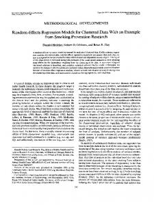
Figure 1 shows the proposed CRAS architecture. The scan cells are clustered according to the compatibility of test stimulus vectors. Two scan cells are said to be compatible if for every stimulus vector, their corresponding logic values are the same or at least one of them is unspecified, otherwise these two scan cells are called incompatible. Y Address Decoder
X Address Decoder
Address
(0, 0)
(0, 1)
(0, 2)
(0, 3)
(1, 0)
(1, 1)
(1, 2)
(1, 3)
(2, 0)
(2, 1)
(2, 2)
(2, 3)
(3, 0)
(3, 1)
(3, 2)
(3, 3)
CRAS0 scan cell CRAS1 scan cell Figure 1
Clustered Random Access Scan Architecture
After being clustered, the scan cells are classified into two types according to the 0-probability and 1-probability of their states. For a scan cell, if the number of its states to be 0 is no less than the number of its states to be 1, the scan cell is classified to CRAS0; otherwise, it is classified to CRAS1. The purpose of this classification is to further reduce the number of scan cells that flip their states during
loading stimulus vectors. The states of the scan cells that are most likely to have the test bit 0 are reset to 0, and the states of the scan cells that are most likely to have the test bit 1 are reset to 1. For the sake of clarity, the scan cells are placed regularly in Figure 1; in practice, however, they can be distributed in the circuit-under-test. As for test response analysis, test responses are compacted with an XOR network and a Multiple-Input Signature Register (MISR). Test response bits of scan cells in a cluster are XORed to form the test response bit of the cluster, and then test response bits of clusters in a row are XORed to form the test response bit of the row. Finally, the test response bit of each row is input to a MISR. The number of registers in the MISR is the number of rows in CRAS. In the MISR, responses are compacted to a signature which will be shifted out at the end of the test. For the sake of clarity, the XOR network and the MISR are no shown in Figure 1. Primary inputs are multiplexed to apply the X and the Y address of the cluster that will be accessed. The address width is ⎡log2 the number of clusters⎤. For example, assume the scan cells have been clustered as shown in Figure 1, the width of the address is 4 with 2 for the X address and 2 for the Y address. Assume a test stimulus vector for clusters is given as, 1010 0110 0010 1101 Then clusters addressed as (0, 1), (1, 2), (1, 3) and (3, 1) are accessed serially, which means address words 0001, 0110, 0111, and 1101 are transformed from the ATE to primary inputs of the circuit-under-test. Once the cluster is accessed, the scan cells in the cluster simultaneously flip their states. Except these four clusters, other clusters will not been accessed, because their states are same as the logic value of the corresponding bits in the test stimulus vector. It is clear to see that the number of stimuli bits stored in the ATE is reduced from 64 to 16. Meanwhile, the clock skew becomes less critical in CRAS, because there is no need to shift the test data along the serially connected scan cells one by one. Moreover, because simultaneously operations on all flip-flops are avoided, the power supply voltage drop is avoided. For the sake of simplicity, the test control signal TC, test clock signal CLK and reset signal RST is not shown in Figure 1, but they are connected to each CRAS scan cell.
2.2.
CRAS Scan Cell Structure
The CRAS0 and CRAS1 scan cells are different from conventional multiplexed DFFs. An AND gate or an OR gate is inserted in front of the MUX as shown in Figure 2. Compared to the scan cell design using a multiplexed DFF, since the AND gate or the OR gate is not on the signal propagation path, the CRAS scan cell design will have the same delay impact as the conventional multiplexed DFF.
On the other hand, the area overhead of CRAS scan cell will be higher than that of the conventional multiplexed DFF, since the CRAS scan cell includes one additional two-input AND or OR gate and the DFF in the CRAS scan cell must be either set-dominant or reset-dominant. RST TC SEL
R D
Q
DI CLK (a) CRAS0 scan cell
RST TC SEL
S D
Q
DI CLK
less global wires and smaller address decoder. The less the number of clusters is, the smaller hardware overhead is. Because the number of clusters depends on the compatibility of the scan cells, we need to optimally cluster the scan cells. However, search the entire scan cell compatibility space to optimally cluster scan cell is computationally prohibitive, we propose a graph coloring based heuristic algorithm for finding an optimal scan cell clustering scheme. The circuit is mapped to an undirected incompatible graph G(S, E) where S is the set of the scan cells, and E is the set of interconnections between pairs of scan cells. If two scan cells are incompatible, there is an edge between them. Thus, the problem of clustering the scan cells can now be defined as: Given an incompatible graph G(S, E), coloring the vertexes of G so as to minimize the number of colors. After the incompatible graph is colored, the scan cells with the same color are grouped into a cluster. s1 s2 s3 s4 s5 s6 s7 s8 v1 0 1 1 1 0 1 0 0 v2 1 U U 1 U 1 U U v3 U 0 U 0 U U U U v4 1 0 U 0 1 U 1 U v5 1 1 U U 1 1 U 1 v6 U 0 0 U 0 U U 1
(b) CRAS1 scan cell Figure 2 CRAS scan cells
(a)
Table 1 shows how TC, the address select signal SEL, and RST together determine the operation mode of a CRAS scan cell, where SEL is the X address signal AND with the Y address signal. When RST =1 and TC=1, the scan cells are in the function mode. Whenever RST =0, CRAS0 scan cells are reset to 0’s and CRAS1 scan cells are reset to 1’s. When RST =1 and TC=0, the scan cells are in the test mode. For a CRAS0 scan cell, once it is selected by the X and the Y address decoders, its state is set to 1; for an CRAS1 scan cell, once it is selected by the X and the Y address decoders, its state is set to 0. The unselected scan cells hold their present states. Table 1
The operation mode of CRAS scan cells
Mode function reset
TC SEL RST 1 U 1 U U 0 selected 0 1 1 test hold 0 0 1 1: logic 1, 0: logic 0, U: the unspecified state
2.3.
CRAS Cluster Algorithm
Unlike [17] that every scan cell has a unique address, in the proposed CRAS architecture, every cluster is assigned a unique address. The scan cells in a cluster share the same address and will be accessed simultaneously. The cluster structure not only reduces the test data volume, but also reduces the routing overhead and area overhead through
s2
s1 s8
s3
s7
s4
s6
s5 (b)
v1 v2 v3 v4 v5 v6
c1 0 1 U 1 1 1 (c)
c2 c3 1 0 1 U 0 U 0 1 1 1 0 0
v1 v2 v3 v4 v5 v6
c1 0 1 1 1 1 1
c2 c3 1 0 1 0 0 0 0 1 1 1 0 0 (d)
(a) Stimulus vectors for the scan cells (b) Colored incompatible graph (c) Stimulus vectors with unspecified bits for the clusters (d) Stimulus vectors without unspecified bits for the clusters Figure 3 An example of clustering the scan cells
Figure 3 illustrates an example of clustering the scan cells. Given the test stimuli shown in Figure 3(a), the incompatible relations can be obtained by comparing bit value of every scan cell. For example, since in every stimulus vector s2 and s3 have the same bits or at least one
of them is unspecified, s2 is compatible with s3. For another example, the bit of s1 and the bit of s2 in v1 is different, so s1 and s2 are incompatible, and an edge is drawn to connect s1 and s2. After the incompatible graph is completed, a heuristic coloring program [18] colors the graph with a minimal number of colors. In this example, as shown in Figure 3(b); the number of colors is 3, so the scan cells are grouped into 3 clusters. In the next section, we will give the approximation value of the minimal number of colors based on the random graph theory. After clustering the scan cells, the original stimuli data will be calculated to obtain the stimuli for the clusters. The specified bits in the original stimuli determine the bits in the stimuli for the cluster. For example, as shown in Figure 3(a) and Figure 3(c), since the specified bit of s4 in v2 is 1, then the bit of c2 in v2 is 1. After the calculation, if there still are unspecified bits in stimulus for the cluster, the unspecified bits will be mapped to 0’s for a CRAS0 cluster, otherwise, the unspecified bits will be mapped to 1’s. For example, the unspecified bits of c3 in Figure 3(c) are mapped to 0’s as shown in Figure 3(d). Finally, the stimuli for clusters without unspecified bits are obtained. The DFT logic shall be tested before testing the circuit-under-test. Since the access mechanism of CRAS is similar to that of static random access memory (SRAM), memory test techniques can be utilized to test CRAS. For instance, MATS++ or March X [19] can be used to test stuck-at faults, address decoder faults and transition faults in the CRAS DFT logic.
3. 3.1.
Theoretical Analysis Random Graph
Assume the unspecified bits in the test stimuli generated by an ATPG tool is randomly distributed, and the number of scan cells |S| is sufficiently large, then the incompatible graph G(S, E) can be considered as a random graph G(|S|, p), where p is the probability that there is an edge between two vertexes, that is, the probability of two scan cells that are incompatible. Let q denote the ratio of the unspecified bits in the test stimuli, then the probability of two scan cells that are compatible is the probability that their corresponding bits in all of N vectors are compatible, N 1 ⎡ ⎤ which equals ⎢ q + q (1 − q ) + (1 − q )(1 − q ) ⎥ . Therefore, 2 ⎣ ⎦ the relationship between p and q is given by, N 1 ⎡ ⎤ p = 1 − ⎢ q + q (1 − q ) + (1 − q )(1 − q ) ⎥ 2 ⎣ ⎦ (1) N 1 ⎡ 2 ⎤ = 1 − ⎢ q + (1 − q ) ⎥ 2 ⎣ ⎦ where N is the number of test vectors.
The chromatic number χ is defined as the smallest number of colors necessary to color the vertexes of a graph so that no two adjacent vertexes have the same color. We
can deduce the approximation value of χ for a random graph according to following theorem [20]. Theorem: Let 0