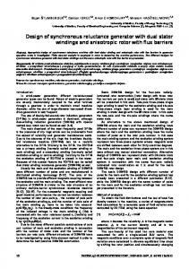
ASEAN J. Sci. Technol. Dev., 34(2): 79 – 94
Thermal Efficient Design of Distributed Memory Generator for Dual-port RAM Using Unidirectional High-performance IO Standard B. DAS* AND M.F.L. ABDULLAH The distributed dual-port RAM offers the high-speed data rate transmission for different memory access modes such as: busy mode; interrupt mode; JTAG mode; master mode; slave mode; and sleep mode, at high-frequency operation. The execution of these modes at high-frequency operation increases the on-chip temperature of distributed dual-port RAM. It might short the distributed dual-port RAM forever. Currently, different techniques have been reported, but significant on-chip temperature consumption is not reduced for distributed dual-port RAM. In this paper, the thermalefficient design for distributed dual-port RAM was achieved using IO standard technique. The distributed dual-port RAM was designed using different IO standards such as; LVTTL IO standard and Mobile_DDR IO standard. It was determined that distributed dual-port RAM was operated at 625 MHz high-frequency operation for busy mode, interrupt mode, JTAG mode, master mode, slave mode, and sleep mode using LVTTL IO standard and Mobile_DDR IO standard. It was observed that for busy mode 53%, for interrupt mode 61%, for JTAG mode 68%, for master mode 62%, for slave mode 59%, and for sleep mode 76% temperature was reduced when distributed dual-port RAM was designed using Mobile_DDR IO standard compared to LVTTL IO standard. The designed distributed dual-port RAM using Mobile_DDR IO standard offered the thermal efficient design solution for different memory access modes at high-frequency data rate transmission that provided the low on-chip temperature consumption. The developed distributed dual-port RAM will be helpful to produce green computing devices. Key words: Distributed dual-port RAM; high-range IO standard; memory access modes; random access memory (RAM); thermal efficient; UltraScaleTM field-programmable gate array
The distributed Memory Generator (DMG) in Xilinx Filed Programming Gate Array core creates the memory out of LUT RAM. This DMG provides the different memory access such as; Read only memory (ROM), Single-Port read access memory (RAM), Dual-port read access memory (RAM). Distributed dual-port RAM in DGM is synchronous with to the clock (CLK) and their read operation can be asynchronous or synchronous concerning either of the two clocks
(CLK or QDPO_CLK). In distributed dual-port RAM in DGM the address, data registers, and resets and clock enables and are optional. It has been defined in Xilink Inc. (2015) that for DGM the maximum frequencies (Fmax) is required for the configuring the memory. The different Fmax for various memory access in defined as; for single-port RAM the memory size is 32×16 at 625 MHz, for Dual port RAM size is 32×16 at 625 MHz. It is discussed in Atmel Corporation
Faculty of Electrical and Electronic Engineering, Universiti Tun Hussein Onn Malaysia, 86400 Parit Raja, Batu Pahat, Johor, Malaysia * Corresponding author (e-mail:
[email protected])
ASEAN Journal on Science and Technology for Development, 34(2), 2017
(2007) that temperature range for distributed dual-port RAM in DGM is varied from –55°C to +125°C depends upon the Fmax used for a specific operation. It also demonstrated in Xilink Inc. (2015) distributed dual-port RAM in DGM there are a different mode of operation such as; busy, interrupt, JTAG, master, slave, and sleep mode. It is also revealed in Xilink (2015) that the core voltage of distributed dual-port RAM in DGM is varied from 1.8 V to 5 V using default IO standard of transistortransistor logic (TTL). It is observed by Das et al. (2016) and Abdullah (2015) that different electronic device, when operated at maximum frequencies, the device temperature increase and this may haul the operation of the electronic devices and may cause the permanent damage to the device. In the case of distributed dualport RAM in DGM, it is very much important to investigate and control the behaviour of temperature variation for distributed dual-port RAM in DGM, when operated in different modes at Fmax of 625 MHz. It has been observed that for distributed dual-port RAM in DGM, the temperature variation for different modes is varied from –55°C to +125°C. This temperature range can be increased for various operation when operated at Fmax of 625 MHz. There are several techniques utilized to control the temperature of electronic devices such as: optical transmitter (Das et al. 2016); video decoders (Bonatto 2011); filters (Pandey et al. 2016). These techniques include, clock gating, voltage scaling, variable frequency, etc. However, each technique has its own advantages and disadvantages. It has been demonstrated by Das et al. (2016), Electronic Industry Alliance (2017), and Xilinx Inc. (2016) that for different variation in suitable IO standard can demonstrate the ability of temperature control of the device by varying the core voltage of field-programmable gate array (FPGA), the
core operating voltage of the device and IO standard voltage selected for the particular device depends on the device configuration. In this paper, the thermal efficient design is demonstrated for distributed dual-port RAM in DGM using high-performance IO standard via UltraScaleTM FPGA. The high-performance IO standard is selected based on the criteria of core voltage of FPGA, and operating voltage of for distributed dual-port RAM in DGM. METHODOLOGY Thermal efficient design for distributed dualport RAM in DGM using high-performance IO standard was designed using different design steps as demonstrated in Figure 1. In the first design step for distributed dual-port RAM in DGM was designed using Vivado® design suite via VHDL coding by defining the different parameters and configuration for distributed dual-port RAM in DGM. In the second design step, the VHDL based on distributed dual-port RAM in DGM was designed using highperformance IO standard. The IO standard was selected based upon the core voltage of FPGA, an operating voltage for distributed dual-port RAM in DGM. In the third design step, the VHDL-based on distributed dual-port RAM in DGM using high-performance IO standard was tested at maximum frequency operation for different mode of operation for distributed dualport RAM in DGM to analyze the performance of the designed thermal efficient for distributed dual-port RAM in DGM. In the last step, the IO standard that had less temperature recording for distributed dual-port RAM in DGM for the different mode of operation was considered as a thermal efficient design for distributed dual-port RAM in DGM. In the next sub-sections, each design step discussed above is detailed. 80
Bhagwan and Abdullah: Thermal Efficient Design of Distributed Memory Generator for Dual-port RAM
Design of the Distributed Dual-Port RAM in DGM in Xilinx Vivado
Thermal analysia of Design of the Distributed Dual-Port RAM using IO Standard
Design of the Distributed Dual-Port RAM using IO Standard
Thermal Efficient design of Design of the Distributed DualPort RAM
Figure 1. Design steps to developing the thermal-efficient design for distributed dual-port RAM in DGM.
A. Design Step 1. VHDL-based Distributed Dual-port Ram in DGM
Table 1 describes the parameters for distributed dual-port RAM. It is illustrated in
The distributed dual-port RAM in DGM was designed in Xilinx Vivado® Suite using VHDL. The schematic design of distributed dual-port RAM in DGM is shown in Figure 2.
Table 1 that memory depth is of 64 bit and data width is 16 bit for dual port RAM. The port configuration was defined as input was registered and output was non-registered with input clock enabled. The distributed dual-port
The distributed dual-port RAM in DGM in Figure 2 is designed using different parameters as illustrated in Table 1.
RAM was designed using pin configuration that was mentioned in Table 2.
Figure 2. Schematic design of distributed dual-port RAM in DGM via VHDL.
81
Table 1. Protocol parameters for distributed dual-port RAM. Memory configuration Depth
64
Data width
16
Memory type
Dual-port RAM Port configuration
Input option
Registered
Input clock
Enabled
Dual-port address
Registered
Input option
Non-registered
Table 2. Port description for designing the Distributed dual-port Ram (Xilinx Inc. 2015) Pin configuration d[p:0]
IO direction
Details
Input data
The input was written into the memory for dual-port RAMs.
a[n:0]
Input address
On dual-port memories, it defined memory location written to, and memory location read out on the SPO[P:0] outputs.
dpra[n:0]
Input
Dual port RAMs and defined memory location read out on the DPO[P:0] outputs.
spo[p:0]
Output
Non-registered single-port output bus. Non-registered data output bus for ROMs and single-port RAMs. One of two non-registered output buses on dual-port RAMs.
dpo[p:0]
Output
Non-registered dual/simple dual-port output bus. One of the non-registered data output buses for dual-port and simple dual-port RAMs. Data stored at the address location specified by DPRA[N:0] appears at this port.
Output qdpo[p:0]
Registered dual/simple dual-port output bus. One of two registered output buses on dual-port and simple dual-port RAMs.
82
Bhagwan and Abdullah: Thermal Efficient Design of Distributed Memory Generator for Dual-port RAM
Table 2 cont. Port description for designing the Distributed dual-port Ram (Xilinx Inc. 2015) Pin configuration clk
IO direction
Details
Input
On dual-port RAMs, signal was the write clock and registered clock for single-port input and output registers.
qdpo_clk
Input
On dual-port RAMs, signal was the write clock and register clock for dual-port and simple dual-port RAM input and output registers.
we
Input
Write enabled.
i_ce
Input
Input clock enabled. Signal was present for RAMs which had registered inputs. The clock enabled controls input data register, address registered and WE register.
It was defined that distributed dual-port Ram using VHDL design was operated at Fmax of 625 MHz for different memory access defined as: busy; interrupt; JTAG; master; slave; and sleep mode. It was also revealed (Xiuyuan 2017; Kumar et al. 2015) that the core voltage of distributed dual-port RAM in DGM was varied from 1.8 V to 5 V using default IO standard of transistor-transistor logic (TTL). It was discussed that for different memory access defined as: busy; interrupt; JTAG, master; slave; and sleep mode, the temperature was varied in between –55°C to +125°C depended upon the Fmax. The proposed IO standard technique offered the less temperature variation for IO standard-based distributed dual-port RAM using VHDL design was operated at Fmax of 625 MHz for different memory access defined as: busy; interrupt; JTAG; master; slave, and sleep mode.
interrupt; JTAG, master; slave; and sleep mode was observed at Fmax of 625 MHz using distributed dual-port RAM using VHDL design and IO standard-based distributed dual-port RAM using VHDL design.
Next, the discussion of IO standard-based distributed dual-port RAM using VHDL design is demonstrated. Subsequently thermal analysis for different memory access defined as: busy;
Virtex® UltraScale™ FPGA support many IO standard and a long list is available in (Electricity Industry Alliance (2017)). In this research, authors have selected the
B. Design Step 2: IO standard-based Distributed Dual-port RAM In UltraScale™ FPGA an I/O tile was defined as I/O buffers, I/O logics and I/O delays. Each IOB contained both input and output logic and IO drivers. These drivers could be configured to various I/O standards (Electricity Industry Alliance 2017). The IO standard based schematic diagram of distributed dualport RAM demonstrated using Figure 3. It is defined in Figure 3 that device configuration was changed by adding the IO standard and its related operating voltage in VHDL-based distributed dual-port RAM.
83
ASEAN Journal on Science and Technology for Development, 34(2), 2017
Figure 3. Schematic design of IO-based distributed dual-port RAM in DGM via VHDL.
unidirectional IO standards that meet the requirements for distributed dual-port RAM in DGM via VHDL. These IO standards are specified in the Electronic Industry Alliance JEDEC (2017). The reason for selecting the unidirectional IO standard for distributed dual-port RAM in DGM via VHDL is that unidirectional offers the program in simple mode without handshaking, and secondly the unidirectional IO standards offers the highrange (HR) IO standard that is suitable for distributed dual-port RAM in DGM via VHDL because for distributed dual-port RAM in DGM via VHDL for different memory access modes at Fmax of 625 MHz, the temperature becomes very high.
Double Data RAM (Mobile_DDR (Low-power DDR); and many more. These unidirectional IO standards are further divided in to high range (HR) and high performance (HP) category. It was already discussed in the above discussion that for distributed dual-port RAM, the HR IO standard was required in order to reduce the temperature for different memory access modes. The above unidirectional HR IO standards for distributed dual-port RAM were categorized as: LVTTL which were HR IO standard, and mobile_DDR. (1) Low Voltage Transistor —Transistor Logic (LVTTL) LVTTL is an IO standard for 3.3 V application that uses a single-ended CMOS input buffer and a push-pull output buffer at 3.3 V output source voltage (VCCO). The syntax for changing the IO standards from default to user defined IO standards (LVTTL) is:
There are different types of unidirectional IO standards are which available such as: low voltage transistor transistor logic (LVTTL); low voltage complementary metal-oxide semiconductors (LVCMOS); low-voltage digitally controlled impedance (LVDCI); high-speed low-voltage digitally controlled impedance (HSLVDCI); high-speed transceiver logic (HSTL); high speed unterminated logic (HSUL); pseudo open drain (POD); Mobile
84
a) Attribute IOSTANDARD : string; Attribute IOSTANDARD of IDIOA0 : label is- “LVDCI_15”;
Bhagwan and Abdullah: Thermal Efficient Design of Distributed Memory Generator for Dual-port RAM
C. Design Step 3: Performance Analysis of Distributed Dual-port RAM Using Proposed IO standard Technique
b) Attribute IOSTANDARD : string; Attribute IOSTANDARD of IDIOA0 : label is- “LVTTL_33”;
The thermal performance analysis for the designed distributed dual-port RAM was observed for Fmax of 625 MHz for different memory access mode such as: busy; interrupt; JTAG; master; slave; and sleep mode. This thermal analysis was demonstrated for IO standard based VHDL-based distributed dualport RAM. The thermal analysis is executed using on-chip device temperature for different operations.
(2) Mobile Double Data RAM (MOBILE_ DDR) The mobile_DDR IO standard is for DDR memory buses. Mobile_DDR is defined by the JEDEC I/O standard JESD209A. It is a 1.8 V single-ended I/O standard that eliminates the need for VREF and VTT voltage supplies. The syntax for changing the IO standards from default to user defined mobile_DDR IO standard is:
(1) Thermal Analysis of Distributed dualport Ram for Fmax of 625 MHz via LVTTL IO standard
a) Attribute IOSTANDARD : string; Attribute IOSTANDARD of IDIOA0 : label is- “LVDCI_15”;
The performance of the distributed dual-port RAM is analyzed for Fmax of 625 MHz for LVTTL IO standard by measuring the onchip device temperature for different memory access mode such as: busy; interrupt; JTAG, master; slave; and sleep mode. The LVTTL was configured for the reference voltage of 3.3 V. Therefore the LVTTL syntax would be changed to LVTTL_33. The on-chip device temperature was measured concerning specific mode of operation of distributed dual-port RAM. The on-chip device temperature was measured regarding different mode of operation such as: busy; interrupt; JTAG; master; slave; and sleep mode of distributed dual-port RAM at Fmax of 625 MHz using LVTTL IO standard. Table 3 defines the on-chip device temperature which was measured concerning different mode of operation such as: busy; interrupt; JTAG; master; slave; and sleep mode of distributed dual-port RAm at Fmax of 625 MHz using LVTTL IO standard.
b) Attribute IOSTANDARD : string; Attribute IOSTANDARD of IDIOA0 : label is- “MOBILE_DDR”;
It was discussed earlier that for distributed dual-port RAM using VHDL design is operated at Fmax of 625 MHz for different memory access such as: busy; interrupt; JTAG; master; slave; and sleep mode and the port voltage varied from 1.8 V to 5 V. It was also discussed that for different memory access such as: busy; interrupt; JTAG, master; slave; and sleep mode the temperature varied between –55°C to +125°C which depended upon the Fmax. Also thermal analysis for different memory access such as: busy; interrupt; JTAG, master; slave; and sleep mode for distributed dual-port RAM is analyzed. This thermal analysis was demonstrated by observing the temperature of different memory access modes such as: busy; interrupt; JTAG; master; slave;, and sleep mode for Distributed dual-port Ram and IO standard based distributed dual-port RAM. 85
ASEAN Journal on Science and Technology for Development, 34(2), 2017
Table 3. Thermal analysis for distributed dual-port RAM using LVTTL IO standard. Mode of Operation of distributed dual-port RAM
Temperature of device observed for mode of operation of distributed dual-port RAM in ºC
Busy mode
45ºC
Interrupt mode
65ºC
JTAG mode
75ºC
Master mode
40ºC
Slave mode
42ºC
Sleep mode
30ºC
the different mode of operation are also shown in Figure 4.
Table 3 defines the temperature of distributed dual-port RAM for specific RAM operation at 625 MHz frequency using LVTTL IO standard. It is illustrated in Table 3 that for distributed dual-port RAM using LVTTL IO standard for busy mode 45ºC device temperature was recorded, for interrupt mode in which external input was responded and the device temperature was recorded as 65ºC. For JTAG mode the device temperature was high 75ºC because the transmitter and receiver synchronization, for master mode 40ºC device temperature was recorded, and for slave mode 42ºC device temperature was observed, the reason for less temperature was that slave mode was slow in response and bus speed for slave mode was also slow, so it consumes less temperature compared to master mode. Finally, in the sleep mode, in which no processing is observed the temperature recorded is of 30ºC. The temperature observed for distributed dualport RAM for specific RAM operation at 625 MHz frequency using LVTTL IO standard for
Figure 4 demonstrates the on-chip temperature consumption for distributed dualport RAM using LVTTL IO standard. It could be observed that when distributed dual-port RAM was operated in JTAG more the thermal consumption for distributed dual-port RAM was very high compared to sleep, slave, interrupt and busy mode. The thermal analysis for distributed dualport RAM is shown in Figure 5 for all memory operations such as: JTAG; sleep; slave; interrupt and busy mode. Figure 5 defines that total onchip temperature consumption for different modes when distributed dual-port RAM was designed using LVTTL IO standard. It was also defined that when distributed dual-port RAM was operated using JTAG mode total on-chip temperature consumption was 25%. For interrupt mode the on-chip temperature 86
Bhagwan and Abdullah: Thermal Efficient Design of Distributed Memory Generator for Dual-port RAM
Mode of operation distributed dualport RAM
On-chip temperature consumption distributed dual-port RAM using LVTTL IO standard
Sleep mode Slave mode Master mode JTAG mode Interrupt mode Busy mode
Tempraure (oC)
Figure 4. On-chip temperature consumption distributed dual-port RAM using LVTTL IO standard. Thermal analysis for distributed dual-port RAM using LVTTL IO standard
Busy mode
Interrupt mode
JTAG mode
Master mode
Slave mode
Sleep mode
Figure 5. Thermal analysis for distributed dual-port RAM using LVTTL IO standard.
consumption was 22%, for busy mode the on-
RAM was designed using LVTTL IO standard the on-chip temperature recorded was 10%.
chip temperature consumption recorded was 15%. For master and slave mode the on-chip
In the next section, the thermal analysis for distributed dual-port RAM using Mobile_DDR IO standard is discussed.
temperature consumption it was 14%. Finally for sleep mode, when distributed dual-port 87
ASEAN Journal on Science and Technology for Development, 34(2), 2017
(2) Thermal Analysis of distributed dual-port RAM for Fmax of 625 MHz via mobile_DDR IO standard
Table 4 shows the temperature of distributed dual-port RAM for specific RAM operation at 625 MHz frequency using mobile_ DDR IO standard. It is shown in Table 4 that for distributed dual-port RAM using Mobile_DDR IO standard for busy mode 21ºC device temperature was attained, for interrupt mode in which external input was responded and the device temperature was recorded as 65ºC. For JTAG mode the device temperature was high, 25ºC because the transmitter and receiver synchronization, for master mode 14ºC device temperature was recorded, and for slave mode 17ºC device temperature was observed, the reason for less temperature was that slave mode was slow in response and bus speed for slave mode was also slow, so it consumed less temperature compared to the master mode. Finally, in the sleep mode in which no processing was observed the temperature recorded was 7ºC. The temperature observed for distributed dual-port RAM for specific RAM operation at 625 MHz frequency using mobile_DDR IO standard for a different mode of operation is also shown in Figure 5.
The performance of the distributed dualport RAM analyzed for Fmax of 625 MHz for mobile_DDR IO standard by measuring the on-chip device temperature for different memory access mode such as: busy; interrupt; JTAG; master; slave; and sleep mode. The mobile_DDR IO standard is configured for the reference voltage of 1.8 V. Therefore the LVTTL syntax will be changed to mobile_DDR.The onchip device temperature is measured regarding specific mode of operation of distributed dualport RAM. The on-chip device temperature was measured concerning of different mode of operation such as: busy; interrupt; JTAG; master; slave; and sleep mode of distributed dual-port RAM at Fmax of 625 MHz using Mobile_DDR IOStandard. Table 4 defines the on-chip device temperature is measured regarding different mode of operation such as: busy; interrupt; JTAG; master; slave; and sleep mode of distributed dual-port RAM at Fmax of 625 MHz using mobile_DDR IO Standard.
Table 4. Thermal analysis for distributed dual-port RAM using Mobile_DDR IO standard. Mode of operation of distributed dual-port RAM
Temperature of device observed for mode of operation of distributed dual-port RAM in ºC
Busy mode
21ºC
Interrupt mode
25ºC
JTAG mode
24ºC
Master mode
15ºC
Slave mode
17ºC
Sleep mode
7ºC
88
Bhagwan and Abdullah: Thermal Efficient Design of Distributed Memory Generator for Dual-port RAM
temperature consumption was 14%. Finally, for sleep mode, when distributed dual-port RAM was designed using LVTTL IO standard the on-chip temperature recorded was 6%.
Figure 6 demonstrates the on-chip temperature use for distributed dual-port RAM using Mobile_DDR IO standard. It could be observed that when distributed dual-port RAM was operated in JTAG the thermal use for distributed dual-port Ram was very high compared to sleep, slave, interrupt and busy mode.
It could be analyzed that when distributed dual-port RAM was operated at 625 MHz for different memory access modes using LVTTL IO standard the temperature consumption was compared to distributed dual-port RAM was operated at 625 MHz for various memory access modes using Mobile_DDR IO standard. It was interesting to note that the total on-chip temperature analysis between LVTTL IO standard and Mobile_DDR IO standard for distributed dual-port RAM was compared using Figure 4 and Figure 7, respectively. It could be analyzed that temperature consumption of distributed dual-port RAM using Mobile_ DDR IO standard was less compared to the distributed dual-port RAM using LVTTL IO standard. It was observed that major temperature consumption was reduced for
The thermal analysis for distributed dualport Ram is shown in Figure 7 for all memory operations such as: JTAG; sleep; slave; interrupt; and busy mode. Figure 7 defines that total onchip temperature consumption for different modes, when distributed dual-port RAM was designed using Mobile_DDR IO standard. It was defined that when distributed dual-port RAM was operated using JTAG mode total on-chip temperature the consumption was 22%. For interrupt mode the on-chip temperature consumption was 23%, for busy mode the onchip temperature consumption recorded was 19%. For master and slave mode the on-chip
Mode of operation distributed dualdual-port RAM
On-chip temperature consumption distributed dual-port RAM using Mobile_DDR IO standard
Sleep mode Slave mode Master mode JTAG mode Interrupt mode Busy mode
Tempraure (oC)
Figure 6. On-chip temperature consumption distributed dual-port RAM using Mobile_DDR IO standard.
89
ASEAN Journal on Science and Technology for Development, 34(2), 2017
Thermal analysis for distributed dual-port RAM using Mobile_DDR IO standard
Busy mode
Interrupt mode
JTAG mode
Master mode
Slave mode
Sleep mode
Figure 7. Thermal analysis for distributed dual-port RAM using Mobile_DDR IO standard.
sleep mode for distributed dual-port RAM using Mobile_DDR IO standard compared to distributed dual-port RAM using LVTTL IO standard. In this section, the thermal analysis was discussed. Next, the results were presented for proposed thermal efficient distributed dualport RAM. It analyzed that proper selection of IO standards may yield reduction in thermal consumption for distributed dual-port RAM.
such as: busy mode; interrupt mode; JTAG mode; master mode; slave mode, and Sleep mode. It was defined that for these memory access modes for distributed dual-port RAM using LVTTL IO standard the temperature consumption recorded for busy mode, interrupt mode, JTAG mode, master mode, slave mode, and sleep mode was 45ºC, 65ºC, 75ºC, 40ºC, 42ºC, and 30ºC respectively, as demonstrated in Figure 8. It could also be analyzed that when distributed dual-port RAM was operated at 625 MHz using mobile_DDR IO standard for different memory access modes such as: busy mode; interrupt mode; JTAG mode; master mode; slave mode; and sleep mode, the temperature consumption recorded for distributed dual-port RAM was 21ºC, 25ºC, 24ºC, 15ºC, 17ºC, and 7ºC respectively, as shown in Figure 8.
RESULTS AND DISCUSSION In this paper, thermal efficient design for distributed dual-port RAM was proposed using high range IO standard. The IO standard was selected according to the specification of for distributed dual-port RAM and UltraScale™ FPGA. For distributed dual-port RAM it was tested for 625 MHz maximum frequency using LVTTL IO standard and mobile_DDR IO standard for distributed dual-port RAM. It was illustrated that when distributed dual-port RAM was operated at 625 MHz using LVTTL IO standard for different memory access modes
It is demonstrated in Figure 8 that when distributed dual-port RAM is designed using Mobile_DDR IO standard and LVTTL IO 90
Bhagwan and Abdullah: Thermal Efficient Design of Distributed Memory Generator for Dual-port RAM
80
Thermal analysis for designed distributed dual-port RAM LVTTL IO standard
Temprature in (oC)
70
Mobile-DDR IO standard
60 50 40 30 20 10 0 Busy mode
Interrupt mode
JTAG mode Master mode Slave mode Sleep mode
Memory operation for distributed dual-port RAM
Figure 8. Thermal analysis for designed distributed dual-port RAM using LVTTL IO standard and mobile_DDR IO standard.
standard for the maximum frequency of 625 MHz for busy mode memory access mode, the on-chip temperature is reduced for distributed dual-port RAM which is designed using mobile_DDR IO standard compared to LVTTL IO standard. It was analyzed that distributed dual-port RAM designed using mobile_DDR IO standard and LVTTL IO standard, the temperature was reduced from 45ºC to 21ºC for Mobile_DDR IO standard on the contrary to LVTTL IO standard-based design for distributed dual-port RAM. It was also determined that 53% on-chip temperature consumption was reduced for distributed dual-port RAM using Mobile_DDR IO standard paralleled to LVTTL IO standard.
compared to LVTTL IO standard for distributed dual-port RAM. It was determined that 61% on-chip temperarure consumption was reduced using Mobile_DDR IO standard for distributed dual-port RAM compared to LVTTL IO standard for distributed dual-port RAM. When distributed dual-port RAM was operated at 625 MHZ for JTAG mode of memory access mode using Mobile_DDR IO standard and LVTTL IO standard, the on-chip temperature was reduced from 75ºC to 24ºC, for distributed dual-port RAM using Mobile_DDR IO standard compared to the distributed dual-port RAM using LVTTL IO standard. It was calculate that on-chip temperature consumption of 68% was reduced for JTAG mode for distributed dualport RAM using Mobile_DDR IO standard compared to distributed dual-port RAM using LVTTL IO standard design.
Distributed dual-port RAM, when operated at 625 MHz using Mobile_DDR IO standard and LVTTL IO standard for interrupt mode, the on-chip temperature consumption was reduced from 65ºC to 25ºC using Mobile_DDR IO standard for distributed dual-port RAM
Distributed dual-port RAM using Mobile_ DDR IO standard and LVTTL IO standard was operated at 625 MHz for master mode. It 91
ASEAN Journal on Science and Technology for Development, 34(2), 2017
was observed that temperature consumption fell from 40ºC to 15ºC using Mobile_DDR IO standard compared to LVTTL IO standard. It was determined that 62% temperature reduction was achieved for distributed dualport RAM using Mobile_DDR IO standard. Distributed dual-port RAM using Mobile_ DDR IO standard and LVTTL IO standard is operated at 625 MHz for master mode, It was observed that temperature consumption fell from 40ºC to 15ºC using Mobile_DDR IO standard compared to LVTTL IO standard. It was determined that 62% temperature reduction was achieved for distributed dual-port RAM using mobile_DDR IO standard. Distributed dual-port RAM using Mobile_DDR IO standard and LVTTL IO standard was operated at 625 MHz for master mode, It was observed that temperature consumption fell from 40ºC to 15ºC using Mobile_DDR IO standard compared to LVTTL IO standard. It was determined that 62% temperature reduction was achieved for distributed dual-port RAM using Mobile_DDR IO standard. Similarly, when distributed dualport RAM was operated at 625 MHz for slave mode using mobile_DDR IO standard and LVTTL IO standard, the temperature reduction was attained form 42ºC to 17ºC using Mobile_ DDR IO standard. It was calculated that when distributed dual-port RAM was operated at 625 MHz for slave mode using Mobile_DDR IO standard reduced the 59% temperature consumption compared to the distributed dualport RAM which was operated at 625 MHz for slave mode using LVTTL IO standard .
It was analyzed that for distributed dual-port RAM using Mobile_DDR IO standard, the total temperature reduction achieved was of 76% compared to distributed dual-port RAM using LVTTL IO standard. The proposed thermal efficient design of distributed dual-port RAM using Mobile_ DDR IO standard defined that for memory access modes such as: busy mode; interrupt mode; JTAG mode; master mode; slave mode; and sleep mode, the on-chip temperature consumption was less compared to distributed dual-port RAM using LVTTL IO standard. It was analyzed that for busy mode (53%), for interrupt mode (61%), for JTAG mode (68%), for master mode (62%), for slave mode (59%), and for sleep mode (76%) temperature was reduced, when distributed dual-port RAM was designed using Mobile_DDR IO standard compared to LVTTL IO standard. It was observed that distributed dual-port RAM using Mobile_DDR IO standard had less onchip temperature consumption for busy mode, interrupt mode, JTAG mode, master mode, slave mode, and sleep mode memory access modes compared to distributed dual-port RAM using LVTTL IO standard, the reason for the less temperature consumption is that Mobile_DDR IO standard had the operating voltage of 1.8 V and LVTTL IO standard had the operating voltage of 3.3 V. It was also defined that the distributed dual-port RAM could operate from 1.8 V to 3.3 V, and the core voltage of the UltraScale™ FPGA was 1.8 V. When the distributed dual-port RAM was operated at 625 MHz for different memory access mode (busy mode, interrupt mode, JTAG mode, master mode, slave mode, and sleep mode) using LVTTL IO standard, the operating voltage of IO standard was more than
Finally, when distributed dual-port RAM was operated for sleep mode using both IO standard mobile_DDR and LVTTL, the temperature was reduced. It was observed that the temperature was reduced from 30ºC to 7ºC for distributed dual-port RAM using Mobile_ DDR IO standard compared to distributed dual-port RAM using LVTTL IO standard. 92
Bhagwan and Abdullah: Thermal Efficient Design of Distributed Memory Generator for Dual-port RAM
the core voltage of UltraScale™ FPGA and also maximum voltage range of distributed dual-port RAM, due to this leakage current exceeded and the on-chip temperature was increased for the busy mode, interrupt mode, JTAG mode, master mode, slave mode, and sleep mode.
provide the thermal efficient design for memory access modes for high-frequency data rate transmission. CONCLUSION AND FUTURE WORK The thermal-efficient design for distributed dual-port RAM using Mobile_DDR IO standard was achieved for existing distributed dual-port RAM. The distributed dual-port RAM was operated at 625 MHz high-frequency operation for different memory access modes (busy mode, interrupt mode, JTAG mode, master mode, slave mode, and sleep mode) using LVTTL IO standard and Mobile_DDR IO standard. It was observed that the temperature for busy mode (53%), interrupt mode (61%), for JTAG mode (68%), master mode (62%), slave mode (59%), and sleep mode (76%) was reduced when distributed dual-port RAM was designed using Mobile_DDR IO standard compared to LVTTL IO standard. It was concluded that the distributed dual-port RAM using Mobile_DDR IO standard could be operated at less temperature for different memory access modes (busy mode, interrupt mode, JTAG mode, master mode, slave mode, and sleep mode) compared to distributed dual-port RAM using LVTTL IO standard for all memory access modes. The designed distributed dual-port RAM using Mobile_DDR IO standard offered the thermal efficient design solution for different memory access modes (busy mode, interrupt mode, JTAG mode, master mode, slave mode, and sleep mode) at high-frequency data rate transmission. The designed distributed dual-port RAM using mobile_DDR IO standard could be utilized for other memory access mode as well. In the future, distributed dual-port RAM could be optimized for more higher frequency than 625 MHz and for additional memory access modes.
It was also observed that distributed dualport RAM for different memory access mode (busy mode, interrupt mode, JTAG mode, master mode, slave mode, and sleep mode) operated at 625 MHz using Mobile_DDR IO standard the operating voltage of IO standard was equal to the core voltage of UltraScale™ FPGA and also fell in minimum voltage range of distributed dual-port RAM, due to this leakage current was very low and the on-chip temperature was also low for busy mode, interrupt mode, JTAG mode, master mode, slave mode, and sleep mode compared to on-chip temperature consumption for distributed dualport RAM using LVTTL IO standard. According to Xiuyuan (2017) the temperature consumption for 10.2% while reducing dynamic energy consumption on the L2 cache by 9.5% is achieved. Kumar (2015) has demonstrated energy efficient RAM, but the temperature consumption is limited to 25ºC – 50ºC, which is practically high. It has been demonstrated that the designed distributed dualport RAM which offered the less temperature consumption of 20ºC to 05ºC at high-frequency operation for different memory modes compared to existing work. The developed device offered the high-frequency operation for distributed dual-port RAM for memory access modes (busy mode, interrupt mode, JTAG mode, master mode, slave mode, and sleep mode) at low temperature using Mobile_DDR IO standard. The designed Distributed dual-port Ram using Mobile_DDR IO standard would 93
ASEAN Journal on Science and Technology for Development, 34(2), 2017
AKNOWLEDGEMENT
Das, B, Abdullah, MFL, Shahida, MSN, Bukhsh, Q & Pandey, B 2016, ‘Temperature control of pseudo noise generator-based optical transmitter using airflow and heat sink profile at high speed transceiver logic IO standard’, Journal of Automation and Control Engineering, vol. 4, pp. 28–32.
This work was supported by the Optical Communication Research Group, Faculty of Electrical and Electronic Engineering, Universiti Tun Hussein Onn Malaysia, Malaysia. We are thankful to Faculty of Electrical and Electronic Engineering, Universiti Tun Hussein Onn Malaysia, Malaysia for encouraging us in this work.
Electronic Industry Alliance 2017, IO standards, [Online]. viewed 17 March 2017, . Kumar, A, Sharma, GK, Kumar, A, Agrawal, T & Srivastava 2015, ‘Design of energy efficient random access memory circuit using stub series terminated logic I/O standard on 28 nm FPGA’, Asian Journal of Science and Technology, vol. 6, no. 8, pp. 1699–1706.
Date of receipt: June 2017 Date of acceptance: July 2017 REFERENCES Abdullah, MFL, Das, B & Shahida, MSN 2015, ‘Temperature regulations of pseudo noise generator based optical transmitter using airflow and heat sink profile’, International Journal of Materials, Mechanics and Manufacturing, vol. 5, pp. 64–67.
Pandey, B, Das, B, Kaur, A & Kumar, T 2016, ‘Performance evaluation of FIR filter after implementation on different FPGA and SOC and its utilization in communication and network’, Wireless Personal Communications, pp. 1–15.
Atmel Corporation 2017, Rad. tolerant high speed 8 Kb × 16 dual port RAM, San Jose, California, United States; viewed 27 April 2017, .
Xilinx Inc. 2015, Distributed memory generator v8.0, in Product guide, Xilinx Inc, San Jose, California, United States; viewed 27 April 2017, .
Bonatto, AC, Soares, AB & Susin, AA 2011, ‘Multichannel SDRAM controller design for H. 264/AVC video decoder’, in 2011 IEEE VII Southern Conference on Programmable Logic (SPL), pp. 137–142.
Xilinx Inc. 2017, SelectIO resources, in UltraScale™ architecture, Xilinx Inc, San Jose, California, United States; viewed 17 March 2017, .
Das, B & Abdullah, MFL 2016, ‘Low power design of high speed communication system using IO standard technique over 28 nm Chip’, IGI Publisher. Das, B, Abdullah, MFL, Shahida, MSN & Chowdhry, B 2016, ‘Energy efficient design of 100 Gb/s optical DPSK transmitter design using UltraScale™ FPGA’, Indian Journal of Science and Technology, vol. 9, pp. 1–7.
Xiuyuan, B 2017, ‘Circuit and architecture codesign of STT-RAM for high performance and low energy’, PhD thesis, University of Pittsburgh. 94