TuBB3 4:30 PM – 4:45 PM
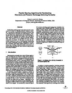
Thermally Active 4×4 Non-Blocking Switch for Networks-on-Chip Aleksandr Biberman1, Nicolás Sherwood-Droz2, Benjamin G. Lee1, Michal Lipson2, and Keren Bergman1 1: Department of Electrical Engineering, Columbia University, New York, NY 10027 2: School of Electrical and Computer Engineering, Cornell University, Ithaca, NY 14853
[email protected]; 212-854-2768 Abstract: We demonstrate power penalty measurements through two output ports of a 4×4 nonblocking switch designed for networks-on-chip. We use integrated metal heaters to tune individual rings, and observe how the device scales with data rate. Introduction Multicore processors, which bypass the power constraints of continued single-core frequency scaling, now dominate the commercial market for high-performance processing chips. Amidst the performance gains of these parallel processing systems, comes an associated increase in the strain placed on the interconnection network, which must efficiently provide large bandwidth and low latency for core-to-core and off-chip I/O communications. Photonic networks-on-chip (NoCs) provide a promising solution to these bandwidth and latency demands, in a manner that scales well in terms of power [1]. Enormous improvements in silicon photonic device technology [2–5] have opened the possibility of CMOScompatible optical interconnection networks. To date, all of the necessary devices (e.g. modulators, switches, links, and receivers) have been demonstrated. Before these NoCs are fabricated, however, functional blocks containing midlevel device integration, must be demonstrated and characterized. The structure discussed here, first proposed in [1], combines a number of 1×2 and 2×2 switches, links, and waveguide crossings, to form a non-blocking 4×4 photonic routing switch, which directs an input from any of the four ports to any of the other three available output ports without obstructing the paths of signals incident from other ports. Using this switch, rather than a simpler blocking switch, improves performance and simplifies the network-level routing algorithms necessary to minimize (or entirely eliminate) packet contentions.
Fig. 1. (a) and (b) depict schematic of 4×4 switch with experimental paths highlighted; (c) microscope image of device.
Fig. 2. Diagram of the experimental setup.
electro-optic switches based on the free-carrier plasma dispersion effect in the final version of the switch, here we also employ the thermal tuners to demonstrate static switching between ports. The experimental setup for the bit-error-rate (BER) measurements (Fig. 2) consists of a single tunable laser source, externally modulated with a signal from a pulse pattern generator (PPG) using an NRZ–OOK data format and a 27–1 PRBS pattern. After modulation, the signal travels through a fiber polarizer, selecting the TE mode, and is coupled to and from the silicon chip using tapered fibers. An erbium-doped fiber amplifier (EDFA), tunable grating filter (λ), and variable optical attenuator (VOA) are employed prior to the high-speed receiver (Rx), which consists of a transimpedance amplifier/limiting amplifier pair. The received signal is evaluated using a communications signal analyzer (CSA) and BER tester (BERT). Polarization controllers (PCs) are used throughout. The heaters are tuned by applying a DC voltage bias through vertically coupled probes to on-chip pads, which distribute current to the appropriate ring heater (Fig. 1c).
Device Fabrication and Experimental Setup The 4×4 switch (Fig. 1) was fabricated at the Cornell Nanofabrication Facility on a silicon-on-insulator wafer, using electron-beam lithography and reactive-ion etching. All waveguides, including the microring resonators, have dimensions of 250 nm (width) by 450 nm (height). The gaps between the ring and straight waveguides are 200 nm throughout, and the rings have 20-µm diameters, corresponding to an 8-nm free-spectral range (FSR). The switch utilizes metal heaters, fabricated directly above each ring on top of the oxide over-cladding layer. The metal traces have dimensions of 1 µm (width) by 300 nm (height), and are used to tune the wavelength of the resonator modes in order to mitigate fabrication imperfections. Although we envision nanosecond-scale
978-1-4244-1932-6/08/$25.00 ©2008 IEEE
Fig. 3. Transmission spectra from port S to W spanning two FSRs and showing the device with (thick line) and without (thin line) voltage applied; arrows indicate the tuned mode in each state.
370
Fig. 5. BER versus received power for data rates of 5 Gb/s (top), 10 Gb/s (center), and 12.5 Gb/s (bottom) taken on optical signals passing from port S to ports N and W and for signals bypassing the chip.
The BER curves also confirm an additional power penalty associated with traveling through the microring resonator. Since the passbands of the resonators in this structure are designed for 10 Gb/s data signals, any data rate above 10 Gb/s should quickly degrade due to spectral sideband attenuation of the high-data-rate signal. This is confirmed experimentally by the fact that at data rates of 5 and 10 Gb/s an additional 0.3 dB of power penalty is associated with traveling through the ring (i.e. comparing port N to port W), while at a data rate of 12.5 Gb/s the additional power penalty of passing through the ring resonator increases to about 1.85 dB.
Fig. 4. Traces of 10-Gb/s optical data shown at the input to the switch and upon exiting ports N and W for two switch states (A and B); time scales are 2 ns/div and a 32-point average is used.
A signal incident from port S has three possible output ports (W, N, and E). However, the chip is fabricated with only two opposing edges reserved for waveguide coupling regions. Therefore, two ports (N and W in Fig. 1a and b) interface at one edge and two (S and E) at the other. Because our experimental setup is not yet able to measure multiple ports on a single edge, only two of the three functional outputs of the 4×4 switch are monitored. Traces of optical data from each port are recorded at each switch configuration (Fig. 4) verifying the correct operation of the switch. All the BER curves are measured at the wavelength of 1550 nm. Before each curve is recorded, the signal is first verified to operate error free for both paths S-W and S-N. For each port, a set of BER curves is taken with varying data rates: 5 Gb/s, 10 Gb/s, and 12.5 Gb/s. When no thermal tuning is performed on the microring resonators, the signal bypasses each of the four rings, egressing from port W (Fig. 1a). A set of BER curves is taken at each data rate (Fig. 5). By thermally tuning the necessary ring so that its resonant mode is aligned to the signal wavelength (Fig. 3), the signal is switched to port N. Again, data rate curves are taken, and the back-to-back case is then setup by bypassing the chip, while maintaining the same injection power into the EDFA using another VOA (Fig. 1a).
Conclusion A 4×4 non-blocking switch utilizing thermally tunable microring resonators is fabricated and power penalty measurements are performed for two of its output ports, with varying data rates. The device is designed for data rates of 10 Gb/s, under which it exhibits low power penalty (under 1 dB) for both output ports. KB, AB, and BGL acknowledge support from the DARPA MTO office under contract ARL W911NF-08-10127. The work of ML and NS-D was part of the Interconnect Focus Center Research Program at Cornell University, supported in part by MARCO, Structured Materials Inc. under Grant 41594, and NSF CAREER Grant 0446571. References [1] A. Shacham et al., Hot Interconnects 2007 (Aug 2007). [2] A. Biberman et al., ECOC 2008 P.2.23 (Sep 2008). [3] B. E. Little et al., IEEE Photon. Technol. Lett. 10 (4) 549– 551 (1998). [4] Q. Xu et al., Opt. Express 15 (2) 430–436 (2007). [5] P. Dong, S. Preble, M. Lipson, CLEO 2007, CTuDD2 (2007).
Results As shown by the BER curves in Fig. 5, the power penalty associated with the S-W path is similar (about 0.65 dB) for 5 Gb/s and 10 Gb/s data rates, but increases to about 1.5 dB for the 12.5 Gb/s data rate.
371