Numerous logic circuits based on these emerging technology have been proposed and prototyped in the last years. In this paper, we present an overview and.
Trends on the Application of Emerging Nonvolatile Memory to Processors and Programmable Devices Lionel Torres, Raphael Martins Brum, Luís Vitório Cargnini and Gilles Sassatelli LIRMM - Université Montpellier 2 / CNRS 161, rue Ada - 34095 Montpellier, France E-mail(s): {torres, brum, cargnini, sassatelli}@lirmm.fr Table I: Comparison of NVM technologies [1], [18], [19]
Abstract—A number of non-volatile memory technologies (NVMs) emerged in the past years. They promise to cope with limitations of standard memory technologies, such as scalability and idle power consumption. Numerous logic circuits based on these emerging technology have been proposed and prototyped in the last years. In this paper, we present an overview and current status of these logic circuits and discuss their potential applications in this field. In the first part, this article provides a survey on the application of those memories to programmable devices. The second section is dedicated to the use of NVMs in the processor’s memory hierarchy, where we discuss potential applications based on a preliminary study we performed. Results were obtained using TAS-MRAM NVM technology. Index Terms—NVM, MRAM, RRAM, PCM, FeRAM, FPGA, Cache Memory, Memory-in-logic.
Technology
Min. cell size (F2 )
Endurance (cycles)
Read time (ns)
Write time (ns)
SRAM STT-MRAM Perpend. STT TAS-MRAM ∗ NAND-Flash NOR-Flash FeRAM RRAM PCM
150 20 4 10 22 30 4
1016 1012 104 105 1012 105 1012
2 5 3 30 100E3 15 40 100 12
2 5-30 3 30 1E6 1E3 65 100 100
∗ Data provided by Crocus Technology
I. I NTRODUCTION SRAM has been the dominant technology for building cache memories in processors and programmable logic in FPGAs. It is a fast, yet nowadays very power-hungry variety of memory. DRAM comes next in the hierarchy, serving as a larger but not so fast volatile memory. Finally, in embedded systems and FPGAs, secondary storage is usually made with solid-state devices based on Flash memory. Many obstacles threaten continued scaling of these three technologies. From increasing leakage power to lithography issues, it has been estimated that, by 2018, SRAM, DRAM and Flash technologies will likely be replaced if Moore’s law is to hold [1]. This landscape motivated the appearance of a number of non-volatile memory (NVMs) technologies in the past years. Spin-Transfer Torque Magnetic RAM (STT-MRAM), PhaseChange RAM (PCM) and Resistive RAM (RRAM), among others, are considered by ITRS as the most promising candidates to take over the mainstream market. In Table I, a quick comparison of those technologies is provided. In 2006, we’ve pioneered the use of emerging NVMs (or eNVMs) for FPGAs by employing thermally-assisted switching (TAS) MRAM [2]. Since then, many works on this subject appeared, ranging from proposed architecture-level enhancements to actual circuit implementations [3]–[17]. In the first part of this publication, we review these works, focusing on those which succeeded on demonstrating this application in practice. Section III is dedicated to STT-MRAM applied to embedded processors. We present current results obtained in the literature
978-1-4673-5762-3/13/$31.00 ©2013 IEEE
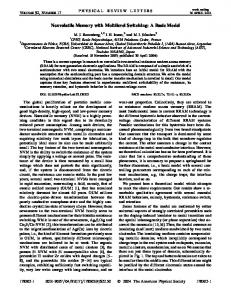
through simulation to explore memory hierarchy based on MRAM. Finally, in section IV, we draw our conclusions and briefly discuss our perspectives on the research of eNVMS for both applications. II. E MERGING NVM S APPLIED TO FPGA S Partial or full FPGA designs have been already fabricated using at least three of these processes: RRAM [3], TASMRAM [5] and REM Relays [8]. To the best of our knowledge, these efforts are summarized in Figure 1. Prototyped designs are summarized in Table II, where some figures of merit are given. Depending on the architecture, these cells are made of several transistors, differently from memory cells. Table II: Figures of selected NVFPGA implementations Ref.
Non-volatile technology
∗Feature size (nm)
†Cell size (F2 )
# of NVMs per bit
[3] [5] [20] [2] [11]
RRAM TAS-MRAM TAS-MRAM TAS-MRAM STT-MRAM
180 130 350 130 90
24 836 800 473 4820
2 2 2 2 2
∗ Associated CMOS process feature size (F). † Referes to the programmable logic cell size.
Stanford’s RRAM based device and our TAS-MRAM prototype are the only complete FPGA architectures based on
101
Architecture and circuit design ArchitecturePower/timing Spice-level level design ↘ estimation ↘ characteriz. ↘ RRAM
Implementation of critical parts Physical Tape-out, layout ↘ validation ↘
Full physical implentation Physical Tape-out, layout ↘ validation ↘ Liauw'12
Liu'08 Guillemenet'08
TAS-MRAM Zhao'07 Chen, C. '10 Zhou'07
NEM Relays
Guillemenet'11
Bruchon'06 Prenat'07 Zhao'09 Chen, C. '12
Sirigir'10 STT-MRAM
Zhao'09 Paul'08
CNT Memristor
PCM
Dong'07 Liu'09 Wang'10 Cong'11 Chen, Y. '10
Chilstedt'09
Figure 1: Survey of NVM-based FPGA implementations.
emerging NVMs taped-out to date. The next subsections analyze these prototypes in further detail. A. RRAM based NVFPGA This prototype consists of a traditional island-style FPGA, fabricated in 180nm CMOS technology, on top of which the programmable resistors are integrated. Apart from the configuration memory, all other parts are constructed purely with CMOS transistors. The memory array is interleaved with the CMOS logic throughout the tile. Write drivers, row and columns decoders and sense amplifiers are shared by the FPGA tiles. Memory cells are constructed using a 1T2R topology, in which two programmable resistances (or PRs) behave as a voltage divider, pulling the bitline – connected to the cell through the access transistor – up or down. RRAM PRs are small when compared to the CMOS feature size, allowing for an optimized cell surface of only 24 F2 . Its operation has been fully demonstrated. Mapping a 4-bit LFSR resulted in a maximum operating frequency of 250MHz while consuming 39.6mW (at 1.8V supply). B. TAS-MRAM based NVFPGA Zhao and his team (IEF/Univ. Paris-Sud XI) suggested a TAS-MRAM based implementation of multi-context LUTs [7]. They also implemented a prototype on CMOS 350nm and TAS-MRAM 120nm, but no further details are mentioned in their publication. In this same project, Prenat et al., from SPINTEC, fabricated MRAM-based 3-LUTs whose surface is about 6600 µm2 [6]. Guillemenet et al. (LIRMM) [20] taped-out a TAS-MRAM based LUT-3 and some MRAM cells using CMOS 350nm and TAS-MRAM 120nm technologies. These cells measured 98µm2 (or 800 F2 ) and have been succesfully verified in
2011 [5]. Prior this work, Bruchon et al. [2] presented a 473 F2 cell based on CMOS 130nm. We then developed a TAS-MRAM based NVFPGA using a CMOS 130nm technology, combined with Crocus TASMRAM 120nm. It is based on Menta’s soft-core eFPGA implementation [21]. As such, it was adapted to meet standardcells restrictions. For instance, routing channels were made unidirectional. At expense of flexibility, this allows for a simpler organization, as SBOXes can be implemented using standard multiplexers, and connect blocks (CB) are no longer required. Each configuration bit is implemented both in CMOS (using standard flip-flops, or FFs) and in TAS-MRAM (using nonvolatile latches, or NVLs). These FFs are also used to control whether their associated NVL’s MTJ must be heated prior to the writing operation. A unique feature of our implementation is the double-context provided by these two elements. Once NVLs are set, a new bitstream can be loaded into the FFs. At any time, the FPGA can be switched between volatile and non-volatile memory. Peripheral circuits include magnetic-field generators and heat control. No sense-amplifier is needed, as NVLs are able to drive a reasonable capacitance. Blocks of 64 to 68 NVLs share a single field-current generator, saving area and reducing power consumption during write operations. Current generators must produce at leat 15mAper block, a drawback of this technology. While standard-cells can operate with voltages as low as 1.2 V, generators required at least 2.5 V. Memory cells’ dimensions are 2.87 by 4.92µm, or 836 F2 , less than half of their CMOS flip-flop counterparts. A current generator occupies 20,000 F2 . This prototype has been successfully taped-out in 2012. Practical results will be published in the coming months.
102
C. STT-MRAM based NVFPGA Zhao et al., from IEF/Université Paris-Sud 11, provide a complete STT-MRAM based FPGA organization in RTL-level [11]. The corresponding memory cells were designed in a CMOS 90nm technology, having an area of 4820 F2 . These cells were not yet reported as validated. Paul et al., from Case Western Reserve University, propose a 2-transistor based voltage sensing mechanism in order to replace standard SRAM cells in the CLBs [12]. Static power consumption became a concern, as the cell is based on a voltage divider made of two magnetic junctions. These results are obtained by means of simulation, and gains of 40% in area are claimed, provided that the assumption of 25 F2 per magnetic junction is valid.
Kang et al. [23] evaluated perpendicular STT-MRAM, showing that a write energy as low as 0.27pJ/bit can be obtained, while using a switching time of about 10 ns. Jog et al. [24] demonstrated that replacing 1MB SRAM L2 cache by a 4MB STT-MRAM L2 cache, for same silicon fingerprint, allows to decrease the overall energy of 40% of the memory hierarchy (mostly due to the lower leakage energy), with an average speed-up of 20%. Furthermore, they took advantage of the relationship between retention time and current density, trading speed for volatility. In the same spirit, we are evaluating the use of MRAM in Level-1 caches of microprocessors targeted for the embedded system domain. A preliminary study, based on data gathered from the SimpleScalar simulator running the set of benchmarks Mediabench 1, was developed in [25].
D. NEM-relay based NVFPGA
III. MRAM AND P ROCESSOR A RCHITECTURE MRAM can also be used for building the processor memory hierarchy. As we’ve seen in Table I, even though the MRAM density is around four times higher than the SRAM’s, its access time is between three and ten times higher. In [22], for example, a 2 MB L2 SRAM Cache was replaced with an 8 MB L2 MRAM Cache, using roughly the same silicon fingerprint. In their particular case, the increase on the cache size was not enough to compensate the penalty due to the cache access delay. By employing write buffers and a novel cache access policy, they managed to achieve similar performance while reducing the power consumption by almost 74%. They also present a hybrid MRAM/SRAM cache organization, having 31 sets implemented in MRAM and 1 set implemented in SRAM. The write-intensive data is kept in the SRAM part, in order to mitigate the higher write delay. A method for determining which data is suitable for being placed in the SRAM set is also discussed.
0 -40 -60 -80 128:512
64:256
32:128
16:64
-100 4:16
Carbon nanotubes (CNTs), memristors and phase-change memory (or PCM) were also investigated [13]–[17]. Even though there is a growing interest in these technologies, these works are currently limited to electrical simulations, as none of these processes are yet available for mid-scale prototyping. We recognize, however, that most of these ideas can be easily adapted for the most developed non-volatile memories, especially with those who share the switching resistance principle.
Best
-20
1:4
E. Memristor, CNT and PCM based NVFPGAs
Average
20
2:8
MRAM CPI Penalty (%)
Worst
8:32
Taking a different approach, Chen et al. (Stanford University) presented a programmable routing crossbar made of nanoelectromechanical (or NEM) relays. They are meant to replace switch boxes (SBs) and connection blocks (CBs), usually made with CMOS. Their prototype consisted of a 2by-2 crossbar design with nanorelays more than 2µm longer. While operational, on-resistance was shown to be larger than a 100kΩ. In fact, NEM relay technology is not as mature as the other NVMs discussed so far.
Cache Capacity - SRAM:MRAM (KB)
Figure 2: Same-area TAS-MRAM versus SRAM L1 Cache execution time comparison
Under the assumption that MRAM density can be four times higher than SRAM’s, it was shown that, for reasonably sized L1 caches, MRAM arrays cannot be directly used without significant performance decrease (Figure 2, the Figure 2 is a standard deviation, depending of the applications, with an average of all benchmarks). SimpleScalar was modified to comply with the TAS-MRAM timing model, as in [25]. We used an access latency of one clock cycle for SRAM and three clock cycles for TAS-MRAM. Our architecture consisted of a single processor having only Level-1 cache in its memory hierarchy. The main memory has a delay of 1000 cycles for the first random read and 10 cycles for the subsequent burst reads. We varied the cache capacity from 4 KB to 256 KB for both technologies. For the purposes of these experiments, we assumed that the MRAM density is four times the SRAM’s. Given that, we compared the performance of an 8 KB SRAM cache with its 32 KB MRAM-based counterpart. It is shown that, for most benchmarks, they are comparable in terms of performance.
103
Cycles Per Instruction - CPI (less is better)
4
8.72
3 2
unepic
mpeg2enc
512 KB MRAM
mpeg2dec
128 KB SRAM
osdemo
mipmap
epic
djpeg
cjpeg
0
texgen
1
Figure 3: Same-area TAS-MRAM versus SRAM L1 Cache execution time comparison
IV. C ONCLUSIONS In this article, we presented a comprehensive survey of emerging non-volatile memories applied to FPGAs. Despite the fact that most of these technologies are still in a prototypical state, numerous IP blocks were developed and could be adapted and used in the prevailing emerging technology. We have also investigated possible applications of these devices to embedded processors. The use of MRAM for Level1 or Level-2 caches is being explored by several research groups, including ourselves. Current results indicate that it could be an attractive answer for the rising power consumption verified in CMOS circuits. The use of eNVMs opens a new paradigm on the implementation of power-saving mechanisms, as the non-volatility could be explored to power-off the devices whenever they’re idle. In fact, we believe that many other architecture elements in digital systems could benefit of the recent advances in NVM technologies. ACKNOWLEDGMENT The authors wish to acknowledge support from French National Agency for Scientific Research (ANR), through the projects CILOMAG, SPIN and MARS. R EFERENCES [1] (2011) International Technology Roadmap for Semiconductors. [Online]. Available: http://www.itrs.net/Links/2011ITRS/Home2011.htm [2] N. Bruchon, L. Torres, G. Sassatelli, and G. Cambon, “New nonvolatile FPGA concept using magnetic tunneling junction,” in Emerging VLSI Technologies and Architectures, 2006. IEEE Computer Society Annual Symposium on, vol. 00, march 2006, p. 6 pp. [3] Y. Y. Liauw, Z. Zhang, W. Kim, A. Gamal, and S. Wong, “Nonvolatile 3D-FPGA with monolithically stacked RRAM-based configuration memory,” in Solid-State Circuits Conference Digest of Technical Papers (ISSCC), 2012 IEEE International, feb. 2012, pp. 406 –408. [4] M. Liu and W. Wang, “rFPGA: CMOS-nano hybrid FPGA using RRAM components,” in Nanoscale Architectures, 2008. NANOARCH 2008. IEEE International Symposium on, june 2008, pp. 93 –98. [5] Y. Guillemenet, “Logique magnétique pour l’exploration d’architectures reconfigurables,” PhD Thesis, Univ. Montpellier II, 2011, in French. [6] G. Prenat, M. El Baraji, W. Guo, R. Sousa, L. Buda-Prejbeanu, B. Dieny, V. Javerliac, J.-P. NoziERES, W. Zhao, and E. Belhaire, “CMOS/Magnetic Hybrid Architectures,” in Electronics, Circuits and Systems, 2007. ICECS 2007. 14th IEEE International Conference on, dec. 2007, pp. 190 –193.
[7] W. Zhao, E. Belhaire, C. Chappert, B. Dieny, and G. Prenat, “TASMRAM based low power, high speed Run-Time Reconfiguration (RTR) FPGA,” ACM Trans on Reconfigurable Techno. and systems, vol. 2, 2009. [8] C. Chen, W. Lee, R. Parsa, S. Chong, J. Provine, J. Watt, R. Howe, H.-S. Wong, and S. Mitra, “Nano-Electro-Mechanical relays for FPGA routing: Experimental demonstration and a design technique,” in Design, Automation Test in Europe Conference Exhibition (DATE), 2012, march 2012, pp. 1361 –1366. [9] Y. Zhou, S. Thekkel, and S. Bhunia, “Low power FPGA design using hybrid CMOS-NEMS approach,” in Proceedings of the 2007 international symposium on Low power electronics and design, ser. ISLPED ’07. New York, NY, USA: ACM, 2007, pp. 14–19. [10] V. Sirigir, K. Alzoubi, D. Saab, F. Kocan, and M. Tabib-Azar, “Ultralow-Power Ultra-fast Hybrid CNEMS-CMOS FPGA,” in Field Programmable Logic and Applications (FPL), 2010 International Conference on, 31 2010-sept. 2 2010, pp. 368 –373. [11] W. Zhao, E. Belhaire, C. Chappert, and P. Mazoyer, “Spin transfer torque (STT)-MRAM–based runtime reconfiguration FPGA circuit,” ACM Trans. Embed. Comput. Syst., vol. 9, no. 2, pp. 14:1–14:16, Oct. 2009. [12] S. Paul, S. Mukhopadhyay, and S. Bhunia, “Hybrid CMOS-STTRAM non-volatile FPGA: design challenges and optimization approaches,” in Proceedings of the 2008 IEEE/ACM International Conference on Computer-Aided Design, ser. ICCAD ’08. Piscataway, NJ, USA: IEEE Press, 2008, pp. 589–592. [13] S. Chilstedt, C. Dong, and D. Chen, “Design and evaluation of a carbon nanotube-based programmable architecture,” International Journal of Parallel Programming, vol. 37, pp. 389–416, 2009. [14] M. Liu, H. Yang, S. Tanachutiwat, and W. Wang, “FPGA based on integration of carbon nanorelays and CMOS devices,” in Nanoscale Architectures, 2009. NANOARCH ’09. IEEE/ACM International Symposium on, july 2009, pp. 61 –64. [15] W. Wang, T. Jing, and B. Butcher, “FPGA based on integration of memristors and CMOS devices,” in Circuits and Systems (ISCAS), Proceedings of 2010 IEEE International Symposium on, 30 2010-june 2 2010, pp. 1963 –1966. [16] J. Cong and B. Xiao, “mrfpga: A novel fpga architecture with memristorbased reconfiguration,” Nanoscale Architectures, IEEE International Symposium on, vol. 0, pp. 1–8, 2011. [17] Y. Chen, J. Zhao, and Y. Xie, “3D-NonFAR: Three-dimensional nonvolatile FPGA architecture using phase change memory,” in LowPower Electronics and Design (ISLPED), 2010 ACM/IEEE International Symposium on, aug. 2010, pp. 55 –60. [18] W. Kim, S. I. Park, Z. Zhang, Y. Yang-Liauw, D. Sekar, H. Wong, and S. Wong, “Forming-free nitrogen-doped AlOX RRAM with sub-uA programming current,” in VLSI Technology (VLSIT), 2011 Symposium on, june 2011, pp. 22 –23. [19] H. Yoda, S. Fujita, N. Shimomura, E. Kitagawa, K. Abe, K. Nomura, H. Noguchi, and J. Ito, “Progress of STT-MRAM Technology and the Effect on Normally-off Computing Systems,” in Electron Devices Meeting, 2012. IEDM Technical Digest. IEEE International, dec. 2012. [20] Y. Guillemenet, L. Torres, G. Sassatelli, N. Bruchon, and I. Hassoune, “A non-volatile run-time FPGA using thermally assisted switching MRAMS,” in Field Programmable Logic and Applications, 2008. FPL 2008. International Conference on, sept. 2008, pp. 421 –426. [21] Menta eFPGA. [Online]. Available: http://menta.fr/efpga_core_ip.html [22] G. Sun, X. Dong, Y. Xie, J. Li, and Y. Chen, “A novel architecture of the 3D stacked MRAM L2 cache for CMPs,” in High Performance Computer Architecture, 2009. HPCA 2009. IEEE 15th International Symposium on, feb. 2009, pp. 239 –249. [23] K. Lee and S. Kang, “Development of Embedded STT-MRAM for Mobile System-on-Chips,” Magnetics, IEEE Transactions on, vol. 47, no. 1, pp. 131 –136, jan. 2011. [24] A. Jog, A. Mishra, C. Xu, Y. Xie, V. Narayanan, R. Iyer, and C. Das, “Cache revive: Architecting volatile STT-RAM caches for enhanced performance in CMPs,” in Design Automation Conference (DAC), 2012 49th ACM/EDAC/IEEE, june 2012, pp. 243 –252. [25] W. Zhao, L. Torres, L. Cargnini, R. Brum, Y. Zhang, Y. Guillemenet, G. Sassatelli, Y. Lakys, J. Klein, D. Etiemble et al., “High Performance SoC Design Using Magnetic Logic and Memory,” in VLSI-SoC: Advanced Research for Systems on Chip. Springer Boston, 2012, pp. 10–33.
104