profile of 1557. Modelling ofthe quantum well subband energy levels was carried out using the envelope function approximation in which the energy states are described using a three-band Kane k p approximation that takes into account the effect of band nonparabolicity and strain. We used this model to design structures each with an n = I to n = 2 transition at about 3.6 pm and to ascertain that all the samples have the same number of states in the well (three). . 7
transition in sample 1557 cannot he due to an increase in oscillator strength for this transition. It has previously been proposcd that reduction in the well bandgap partially relaxes thc elcctric field vector selection rule [SI. Altcmatively the step itself may have.a similar effect due to the contribution to the energy states from two different materials. Relaxation of the selection rule in a conventional stepped well has been theoretically analysed in [9]. (It is interesting to note that here we observe absorption enhancement despite the n = 1 IcvcI not being confined with the InGaAs alone.)
D
E 6
5
$
4
0 8
3
.8
B
2
e
1
f!
Conclusion: We have demonstrated an enhancement in the strength of the n = I to n = 2 intersubband absorption in GaAs DBQWs by introduction of an InGaAs layer. This occurs dcspitc an expcctcd reduction in the oscillator strength for this transition due to other normally forbidden transitions becoming allowed. The enhanced absorption is attributed to relaxation of the electric field vector selection rule.
0
3.0
4.0 1.pm
3.5
4.5
5.0
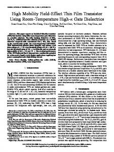
Fig. 2 Room temperature FTIR absorption spectrum of samples 1546, 1551, and 1557 ar Brewsrer angle using p-polwised light Curves are offset for clanry. Dip at 4.25 ~ i m is duc to CO, absorption in infrared beam path
Q IEE 2002 Electronics Letters Online No: 20020261 DOI: I0.I04Y/e1:20020261
13 December 2001
K.T. Lai, S.K. Haywood and R. Gupta (Deparrment ofEngineering, Uniwxyity of Hull, Cottingham Rood, Hull HU6 7R.K United Kingdom) E-mail:
[email protected]
M. Misrous (Department of Electricol Engineering and Electronics. UMISZ PO. Box 88, Manchester M60 IQD, United Kingdom) References
0.1-
0
10
20
30
40
50
60
70
80
90
palariser angle, deg
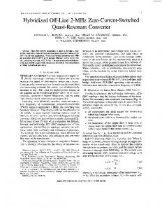
Fig. 3 Normalired n = I to n = Zpeak intensio ugoinsrpolarisrr angle. 0. for rumples 1551 end 1557 room temperature inrersubband absorption was measured in a Bio-Rad FT-3000 Fourier transform infrared spectrometer with a ZnSe wire grid polariser. Since the polarisation selection rule allows only radiation with its electric field vector perpendicular to the plane of the QW to stimulate an intersubband transition [I], the samples were oriented at the Brewstcr angle. The absorption spectrum was then measured using lightp-polarised with respect to the plane of incidence. Fig. 2 shows then = 1 t o n = 2 intersubband absorption for the three samples sh+died. As expected there is an increase in the magnitude of absorption with camer concentration for the two GaAs well samples (1546 and 1551). Significantly increased absorption is observed for the stepped well sample (1557) compared to 1551, even though it has a lower sheet camer density (see Table I). To investigate further the increased absorption in the stepped DBQW, the angle of the polariser was varied from 8= O to 90" thus varying the fraction of p-polarised light in the incident beam. The normalised peak intensities for the stepped well (1557) and the higher-doped GaAs well (1551) are shown in.Fig. 3. According to the selection mlc far light induced interrubband transitions in QWs the absorption should decrease as cas2D under these conditions. The solid line in Fig. 3 indicates this theoretical C U N ~ . The stepped well shows a greater than cos28 dependence of the peak intensity whereas the square well peak intensity drops off much more rapidly with palariser angle. The enhanced absorption in the stepped well and the persistence of the absorption to greater polariser angles indicates a degree of relaxation of the selection rule forbidding normal incidence absorption. Since all the samples have three levels in the well and incorporation of the step is known to increase the oscillator strength ofthe normally forbidden n = I to n = 3 transition [ 6 ] , thc increase in the n = 1 to n Results: The
=z
530
..
'Ouantum-well infrared ohotodetectors'.. J Am/. Phw.. , 1993, 74, pp. G-RXI LENCHYSHYN, L.c., LIU. H.c., BUCHANAN.M., and WASILEU'SKI,~R.: 'Midwavclength infrared detection with In,Gal-,As aAs/Al,,,Gaa.,,As multiple quantum d l structures', Semicond. Sci. Zchriol., 1995, 10, pp. 4 5 4 8 LEVWE. B.F., GUNAPALA. S.D., and KIIPF, R F.: 'Photovoltaic GaAs quantum well infrared detectors at 4.2 pm using indirect AI,Ga,,As barrier', Appl. Phys. Lett., 1991.5R, pp. 1551-1553 LIU, H.c., BUCHANAN. M., and WASILEWSKI. z.R.: 'Short wavelength (I4pm) inhred detectors using intersubband transitions in GaAsbased quantum wells', Appl. Phys. Lett., 1998.83, pp. 6178-6181 NEU,G., CHEN.Y., DEPARIS.C.,and MASSES, J.: 'Improvcmcnt ofthc carrier confinement by double-banier GaAs/AIAs/(AI,Ga)As quantum well stmctu~es',Appl. Phys. Len, 1991,5R,pp. 2111-2113 MIT, Y J , WAN& K.L., KAKUNASIRI, R.P.G., and YUH, P.F.: 'Observation of large oscillator strengths for both 1-2 and 1-3 intersubband transitions of step quantum well', Appl. P h y Lett., 1990, 56, pp. 104&1048 MISSOUS. M.: 'Stoichiometnc low-lempemre GaAs and AIGaAs: a reflection high-energy electron-diffraction study', J Appl. Ph.vs., 1995, 78, pp. 44674471 LIU. F I . ~ . , BUCHANAN, M., and U'ASILEWSKI, Z . R : 'How good is the polanmian selection rule for intersubband transitions', Appl. P h y Lett., 1998, 72. pp. 1682-1684 YUH. P.F., and WANG, K.L.: 'Optical transitions in a step quantum well'. J Appl. Phy.r., 1989, 65, pp. 43774381 LEVWE. B F:
0.5-
Well-driven floating gate transistors A.F. Mondragbn-Torres, M.C. Schneider and E. SinchezSinencio A new layout i t r u ~ t ~ for r e floating gate MOS devices an top of an isolating n-well is proposed. The w d provides the floating device with noise isolation from the subsme and can also be used as an additional input for threshold volwge control or signal modulation
Introduction: Floating gate (FG) transistors are used in both digital and analogue circuits. In digital circuits they are the core of flash memories [ I , 21. For analogue circuits, multiple input (MI) FGMOS devices are used in low voltage applications [3], as analogue memories 141 or as translinear computing elements 151.
ELECTRONICS LEmERS 23rd May 2002
Vol. 38 No. 1 I
~
Traditionally, FG ~ t m ~ hare m laid ~ out on tap of thc substrate. However, it is a common practice to lay out capacitors on top of a well to isolate thc capacitor from substrate noise. Using this principle, we designed a MI-FGMOS transistor with a floating gate on top of an "-well.
Floating gore device: The FG element consists of an electrode surrounded by an insulator, with no direct klectrical connection to any other conductor. The FG electrode acts as the gate of a MOSFET, which serves as the sensor transistor. The potential on the floating gate can be modified either by capacitive coupling with other conductors or by changing the charge stored on the floating gate [I]. In Fig. la, we show the symbol representing an MI-FGMOS transistor, which is a generalisation of a FG device with only one controlling gate. One of the most interesting characteristics of FG devices for analogue circuit design is that the drain current is a function of the weighted sum of voltages at the N conh-olling inputs.
P
cc
Mcosuremenr result.% All the measurements were performed on three-input FGMOS devices fabricated in a 0.35 pm technology with MOSFET channel dimensions W =1.8 pm and L=O.8 pm. Each controlling input capacitor was laid out with an area 3.2 pm x 3 . 2 pm resulting in C j = 8 . 8 ff. The drawn area of the nwell is 12.8 vm x 5.2 pm, For measurement purposes we connected all contrdling inputs together. From now on, Vcc is referred to as the controlling input and a m = CJC, as the total coupling coefficient associated with the controlling input. The determination of the coupling coefficients is based on comparison of measurements taken on both the FG element and a 'dummy cell', which is a reference NMOS transistor with the same channel geomehy as the FG device. To estimate IICG and q v we measure the equivalent subthreshold slope factors n, H~~ and a''' dircctly from the linear portion of the drain current against voltage plots shown in Fig. 2. Referring to (2), wc observe that nr= */a,, where x represents
EL,
CG or W _I
10-3-
""
I
c*b
VS
a
i;
-
I
L 10-1'
b
0
0:2 0.4
0.6
0.8
1.0
10 MFGMOS Vw=O -,DMFGMOS",.=OI
1.2
1.4
1.6
1.8
2.0
vG;vcG:vw. v V, (MOSFEV. iD Ugoinsr ~ i 2 I" ~ . and 1, agoinst Vw (Vcc = 0 MI-FGMOS)
vcc vw=o MI-FCMOS),
To extract the subthreshold slope factors from Fig. 2, we find the regions with an exponential charactenstic and we obtain the values from the definition l i n = Q,d ln(lD)/dVGs, The measured subthreshold slope factors obtained are n = 1.45, nCG=2.1 I and n W = 5 . 6 8 . and the corresponding coupling coefficients are acG=0.69 and air= 0.26.
U
10-3,
c
1044
Fig. 1 MI-FGMOS rransisrur a Symbol
h Equivaleni capacitive modcl c
Layout
V, is additional well input
In Fig. IC, we show the MI-FGMOS layout, including B well beneath the floating gate. In Fig. Ih, we show its capacitive equivalent model. The voltage at the floating gate can be expresscd as N
v,,
=
E a j v , +cwvw + VLQ
(1)
I=,
-0.5
where a,=C,/CT is the ith coupling coefficient, C, represents the capacitance from. the ith controlling input V, to the float& gate and C,is the total capacitance ofthe floating gate. Similarly, aw= Cw/Cris the coupling coefficient from the well input Vw to the floating gate. Vrp is an equivalent voltage due to both the charges stored on the floating gate and to DC voltages at the source and drain that are capacitively coupled to the floating gate. In weak inversion, the current in the drain terminal is ~~
where n is the subthreshold slope factor, 4, is thc thermal voltage, and lo is a constant dependent of technology and geometry 151. The weak inversion region is more convenient to extract the subthreshold factor and thus the coupling coefficients, but the extraction methods are not limited to this level of operation.
4.3
4.1
0.1
0.3
0.5
0.7
0.9
'CG.
Fig. 3 ID uguinst Vcc
In Fig. 3, we show IDagainst V, plots for well voltages Vw from 0 V to 3.3 V in 0.6 V steps. The IOagainst V,, curve shifts to the left as Vwis increased the result is equivalent to a modification ofthe effective threshold voltage G'seen from the controlling gate, according to
where V, is the k s h o l d voltage at the floating gate. We can also express the variation of the threshold voltage by
ELECTRONICS LETTERS 23rd M a y 2002 Vol. 38 No. I I
531
where
Cw is the poly, to n-well thick oxide capacitance. Fig. 3 shows that the threshold (horizontal) shift of the curyes is approximately proportional to the well voltage. Iherefore, one can conclude from (4) that the ratio given by ( 5 ) is almost constant over the whole range of well voltages. Since Ccc is a linear capacitor, one can conclude that Cx,is also linear. This result is the expected one because in our FG device the wcll operates in the accumulation region for the whole range of allowahlc well voltages. The remaining capacitance C, (C&+ C&,+ C , & at the floating gate is
The total input capacitance of the controlling gate estimated by the layout and from manufacturer's spccificatians is Ccc = 26 ff. Then, by using (S), the resulting polyl-to-well capacitance is C w = 10 fF and using (6), the remaining capacitance is Cn = 2ff. Note that the capacitor Cw from well to hulk represents a very important contribution to the total capacitance at the' floating gate.
Conclusion; The new well-driven MI-FGMOS device can he used in applications where the controlling inputs require isolation from the substrate, where the additional n-well input can he used to program the equivalent threshold voltage without altering the hehaviour of the controlling inputs or where modulation of the controlling inputs is required.
0 IEE 2002 Electronics Letters Online No: 20020360 DOI: 10.104Y/e1;20020360
using the discrete Fourier transform (DFT) or fast Fourier transform (FFT) technique has been dcvclopcd, and is referred to as the discrete multi-tone (DMT) modulation. Owing to its high transmission efficiency, DMT has been adopted as the standard modulation for the asymmetric digital subscriber line (ADSL) system. ADSL is a new transmission technology that may provide a 1.5 to 8 Mhit/s data rate over existing local loops. Both rhe frequency division multiplcxing (FDM) scheme and the echo-canceller (EC) scheme are allowed in DMT ADSL [3]. The EC-based structure can have a larger transmission capacity than that of the FDM structure, however, an EC is required. Data driven EC is the most popularly employzd architecture far DSL because of its easy implementation [4]. A traditional EC model is shown in Fig. 1, without the window-gate circuit. The dctailed theory of EC for ADSL is covered in [4] in detail. ADSL EC is generally composed of one frequency-domain EC and a timedomain tail canceller. The frequency-domain EC consists of N adaptive one-tap FIR filters in parallel, where N is the number of suhchannels. The tap-coefficients of the frequency-domain EC can be represented by an N-tuple vector, denoted by H . To maintain a less complex circuit, the least mean square (LMS) algorithm is always employed to update the.tap-coefficients. As H is determined, the timcdomain echo response h can be quickly estimated by an IFFT, denoted by EC-IFFT here. Assuming H and h are both known, the timedomain echo tail can he precisely estimated by performing a shorttime convolution. x
I
4 January 2002
A.F. Mondrag6n-Torres and E. SQnchez-Sinencio (Depurlment of
Electrical Engineering, Texas A d M University, College Slurion, TX, 77840, USA)
Fig. 1 Modified ADSL data driven echo-canceller
E-mail:
[email protected] M.C. Schneider (LCI-Deportamenlo de Engenharia E1L;rrico. Univerxidude Federal de S a m Catorino. CP 476, 88 040 900, Florianbpolis, SC,Brosil) References .IEE9
sfandard
and charactenzarion
Of
Roafing gafc
semiconductor arrays', 9 Feh. 1999 (IEEE Std 1005-1998) PAVAN, P , BE. R., OLIVO. P., and ZANONI, E.: 'Flash memory cellS - an overview', Pmc. IEEE, 85, (8), Aug. 1997 SANCHEZ-SMENCIO, E., and ANDREOU, A,: 'Low-voltage/low power integrated circuits and systems', IEEE Press, Chap. L 1999 HASLER E, MMCH, 8.. and DIoRIO, C.: 'Floating-gate devices: they are not just for digital memories any more'. in Proc. ISCAS '99, 1999, vol. 2, pp. 388-391 MNCH,B., DIORtO.C., HASLER.E,and MEAD.C.: 'Translinear circuits using subthreshold floating-gate MOS transistors', Analog I n t e ~Circuirs ~ Signul Proce.~~. 1996, 9, (2). pp. 167-180
Window-gate for echo canceller of DMT
ADSL S.-W. Wei and H.-Y. Wang A window-gate for the echo-canceller of a discrete multi-tone aiym-
memc digital subscriber line system is presented. This modification can significantlyimprove the convexencc Ofthe echo-canceller in the stamp mining pmcedure as well a i the re-synchronisltinn in splitterless operation.
Inrroducrion: Multicarrier modulation (MCM) has been proved to he one of the optimum modulation techniques for severe distortion channels [I,21. Since the 1980s a digital implementation of MCM
532
Splitterless operation: Integrating plain old telephone services (POTS) with data services is a,necessary requirement in the ADSL system. In the splitterless ADSL operation environment, the equivalent loop impedance seen from thc remote-side varies when thc telephone sets 'hook' on or off In fact. the pulse response of the channel will suddenly change at the instant the telephone hooks On/off Therefore, a fast re-synchronisation operation is necessary when a telephone hooks on/oft In this simulation, the in-home loop model recommended in the G.test standard is employed [ 5 ] . Initially, we suppose the ADSL is working in a normal state and all telephones are hooked on. Then. based on reasonable operation, we assume four different operation modes (Onion; offion;Offioff; onjoft) occur for phone A and phone B. Fig. 2 shows the corresponding ccho channel responses for the four possible different modes where the impedance modelling of telephone hooking onloff follows the models presented in the G.test [SI. In the simulation results shown in Fiy. 2. a test loop T1.601#7 is used as the outdoor loop [3]. Modrfjcd EC: For the EC simulation with traditional structure, i.e. without the window-gate in Fig. 1, we observed that the frguency
domain EC could not immediately locate the exact solution h at the beginning due to the use of the LMS algorithm (an enampk of the learning curve is shown in Fig. 3). This is hecause the vector H cannot be immediately determined and will vary for a short time during the initial period ?f the training operation. Obviously, the time-domain echo response h will also vary so that the echo tail cannot he e2timated correctly. This emor will he passed hack to the estimation of H via the FFT path in the =,--iver, This joint convergence between ? ,+ and h makes the convergence rate slower. Since the tail of the ccho response should be very small and nearly zero due to the operation of the time-domain (TEQ) equaliscr [ 6 ] ,%'e can force part of the echo tail to b e l e r o during the initial training period, i.e. only use the main part of h and discard the tail since it is
ELECTRONICS LETTERS 23rd May 2002
Vol. 38 No. 1 1