Aperstructure, Radar, Digital Radar, Modulator, Demodulator, Transmit/ Receive Module, ... software development of a 2.4 GHz two-element array demonstrator.
NAVAL POSTGRADUATE SCHOOL MONTEREY, CALIFORNIA
THESIS WIRELESSLY NETWORKED OPPORTUNISTIC DIGITAL PHASED ARRAY: SYSTEM ANALYSIS AND DEVELOPMENT OF A 2.4 GHZ DEMONSTRATOR by Eng Choon Yeo December 2006 Thesis Co-Advisors:
David Jenn Donald Walters
Approved for public release; distribution is unlimited
THIS PAGE INTENTIONALLY LEFT BLANK
REPORT DOCUMENTATION PAGE
Form Approved OMB No. 0704-0188
Public reporting burden for this collection of information is estimated to average 1 hour per response, including the time for reviewing instruction, searching existing data sources, gathering and maintaining the data needed, and completing and reviewing the collection of information. Send comments regarding this burden estimate or any other aspect of this collection of information, including suggestions for reducing this burden, to Washington headquarters Services, Directorate for Information Operations and Reports, 1215 Jefferson Davis Highway, Suite 1204, Arlington, VA 22202-4302, and to the Office of Management and Budget, Paperwork Reduction Project (0704-0188) Washington DC 20503.
1. AGENCY USE ONLY (Leave blank)
2. REPORT DATE 3. REPORT TYPE AND DATES COVERED December 2006 Master’s Thesis 4. TITLE AND SUBTITLE Wirelessly Networked Opportunistic Digital Phased 5. FUNDING NUMBERS Array: System Analysis and Development of a 2.4 GHz Demonstrator 6. AUTHOR(S) Eng Choon Yeo 7. PERFORMING ORGANIZATION NAME(S) AND ADDRESS(ES) 8. PERFORMING ORGANIZATION Naval Postgraduate School REPORT NUMBER Monterey, CA 93943-5000 9. SPONSORING /MONITORING AGENCY NAME(S) AND ADDRESS(ES) 10. SPONSORING/MONITORING Office of Naval Research AGENCY REPORT NUMBER Arlington, Virginia 11. SUPPLEMENTARY NOTES The views expressed in this thesis are those of the author and do not reflect the official policy or position of the Department of Defense or the U.S. Government. 12a. DISTRIBUTION / AVAILABILITY STATEMENT 12b. DISTRIBUTION CODE Approved for public release; distribution is unlimited 13. ABSTRACT (maximum 200 words) The concept of a wirelessly networked opportunistic digital phased array radar brings about the added advantages of stealth, enhanced survivability, and maximum maneuverability. The array elements are spread over a wide range of locations on the ship’s hull and superstructure, and the Local Oscillator (LO) and data/control signals are wirelessly transmitted to and from a central computer processor, which also performs as the digital beamformer. As part of the ongoing research effort, this thesis focused on the hardware and software development of a 2.4 GHz twoelement array demonstrator. A system analysis of a generic distributed array radar was done and some key parameters pertaining to the Transmit/Receive (T/R) module and an eight-element array radar were calculated. In addition, the research analyzed the radar waveform properties, sampling and data rates, the digital beamformer concept and requirements, and assessed their impacts on the radar performance. Two Transmit/Receive (T/R) modules were built and a two-element array test bench developed using the various National Instruments Compact Reconfigurable Input and Output (cRIO) and Field Programmable Gate Array (FPGA) modules. The main software, written in LabVIEW, allowed the test bench to demonstrate the proper functionalities of transmission and reception of the T/R modules. The hardware and software code could be extended easily for an eight-element array radar. Lastly, a number of measurements to characterize the T/R module were done. No significant interference between the modulator and demodulator boards inside of the compact T/R module chassis was observed. 14. SUBJECT TERMS Phased Array, Distributed Array Radar, Opportunistic Phased Array, Aperstructure, Radar, Digital Radar, Modulator, Demodulator, Transmit/ Receive Module, Digital Beamforming, Array Demonstrator.
15. NUMBER OF PAGES 92 16. PRICE CODE
17. SECURITY CLASSIFICATION OF REPORT Unclassified
20. LIMITATION OF ABSTRACT
18. SECURITY CLASSIFICATION OF THIS PAGE Unclassified
NSN 7540-01-280-5500
19. SECURITY CLASSIFICATION OF ABSTRACT Unclassified
UL Standard Form 298 (Rev. 2-89) Prescribed by ANSI Std. 239-18
i
THIS PAGE INTENTIONALLY LEFT BLANK
ii
Approved for public release; distribution is unlimited
WIRELESSLY NETWORKED OPPORTUNISTIC DIGITAL PHASED ARRAY: SYSTEM ANALYSIS AND DEVELOPMENT OF A 2.4 GHZ DEMONSTRATOR Eng Choon Yeo Civilian, Ministry of Defence, Singapore B. Eng. (Electrical & Electronic), Nanyang Technological University, 1996 MSc. (Electrical Engineering), National University of Singapore, 2000
Submitted in partial fulfillment of the requirements for the degree of
MASTER OF SCIENCE IN COMBAT SYSTEMS SCIENCE AND TECHNOLOGY
from the
NAVAL POSTGRADUATE SCHOOL December 2006
Author:
Eng Choon Yeo
Approved by:
David Jenn Thesis Advisor
Donald Walters Thesis Advisor
James Luscombe Chairman, Department of Physics iii
THIS PAGE INTENTIONALLY LEFT BLANK
iv
ABSTRACT The concept of a wirelessly networked opportunistic digital phased array radar brings about the added advantages of stealth, enhanced survivability, and maximum maneuverability. The array elements are spread over a wide range of locations on the ship’s hull and superstructure, and the Local Oscillator (LO) and data/control signals are wirelessly transmitted to and from a central computer processor, which also performs as the digital beamformer. As part of the ongoing research effort, this thesis focused on the hardware and software development of a 2.4 GHz two-element array demonstrator. A system analysis of a generic distributed array radar was done and some key parameters pertaining to the Transmit/Receive (T/R) module and an eight-element array radar were calculated. In addition, the research analyzed the radar waveform properties, sampling and data rates, the digital beamformer concept and requirements, and assessed their impacts on the radar performance. Two Transmit/Receive (T/R) modules were built and a two-element array test bench developed using the various National Instruments Compact Reconfigurable Input and Output (cRIO) and Field Programmable Gate Array (FPGA) modules. The main software, written in LabVIEW, allowed the test bench to demonstrate the proper functionalities of transmission and reception of the T/R modules. The hardware and software code could be extended easily for an eight-element array radar. Lastly, a number of measurements to characterize the T/R module were done. No significant interference between the modulator and demodulator boards inside of the compact T/R module chassis was observed.
v
THIS PAGE INTENTIONALLY LEFT BLANK
vi
TABLE OF CONTENTS I.
INTRODUCTION........................................................................................................1 A. BACKGROUND ..............................................................................................1 B. PREVIOUS WORK.........................................................................................3 C. THESIS OBJECTIVE .....................................................................................5 D. THESIS ORGANIZATION............................................................................5
II.
SYSTEM ARCHITECTURE .....................................................................................7 A. WIRELESSLY NETWORKED DISTRIBUTED DIGITAL ARRAY RADAR CONCEPT.........................................................................................7 B. WIRELESS SENSOR NETWORKS ...........................................................10 C. CONFORMAL AND MULTI-FUNCTION ARRAYS ..............................11 D. ADVANCES IN MICROELECTRONICS AND SIGNAL PROCESSING................................................................................................11 1. Field Programmable Gate Arrays (FPGAs)....................................12 2. Direct Digital Synthesis (DDS)..........................................................12 E. DIGITAL BEAMFORMING .......................................................................14 F. TIMING AND SYNCHRONIZATION .......................................................18 1. Wireless LO and Synchronization....................................................18 2. Element Geolocation..........................................................................20
III.
DISTRIBUTED ARRAY RADAR DESIGN AND ANALYSIS............................21 A. T/R MODULE ANALYSIS...........................................................................21 1. Receiver Noise Figure, Effective Temperature and Noise Floor ...21 2. Sensitivity and Dynamic Range ........................................................22 3. Maximum Power Output of T/R Module ........................................23 B. DISTRIBUTED ARRAY RADAR ANALYSIS..........................................23 1. System Noise Temperature and Noise Factor .................................24 2. Radar Range Equation ......................................................................25 Signal-to-Noise Ratio and Detection Range.....................................27 3. 4. Waveform, Sampling Rate and Data Rate ......................................28 5. Digital Beamformer (DBF) Performance ........................................31 6. Transmitter Leakage .........................................................................32
IV.
HARDWARE AND SOFTWARE DEVELOPMENT ...........................................37 A. ELECTRICAL DESIGN OF T/R MODULE..............................................37 1. Power Divider.....................................................................................38 2. RF Cable Assemblies .........................................................................39 3. Optimum AD8346 and AD8347 Settings .........................................40 B. MECHANICAL DESIGN OF T/R MODULE............................................41 C. CONTROLLER AND DATA ACQUISITION SYSTEM .........................42 1. cRIO Embedded System ...................................................................42 2. cRIO Reconfigurable Chassis and Controller.................................43 3. NI-9263 Analog Output Module .......................................................43 4. NI-9215 Analog Input Module..........................................................43 vii
D. E.
5. Software Model ..................................................................................44 6. Arbitrary Waveform Generation .....................................................44 TWO-ELEMENT ARRAY DEMONSTRATOR TEST BENCH.............45 LABVIEW PROGRAM ................................................................................47 1. LabVIEW Project Structure.............................................................47 2. User Interface .....................................................................................48
V.
MEASUREMENTS AND RESULTS ......................................................................51 A. DC POWER CONSUMPTION ....................................................................51 B. INTERFERENCE BETWEEN THE MODULATOR AND DEMODULATOR BOARDS .......................................................................51 1. Transmit Output when Demodulator is On/Off .............................51 2. Receive Output When Modulator is On/Off ...................................53 C. TRANSMIT AND RECEIVE DELAYS......................................................55 1. Transmit Delay...................................................................................55 2. Receive Delay......................................................................................58 D. SIMULTANEOUS TRANSMISSION AND RECEPTION.......................60 1. Simultaneous Transmission ..............................................................60 2. Simultaneous Reception ....................................................................61 E. PHASE ERROR MEASUREMENT............................................................63 F. S11 OF T/R MODULE RF PORT .................................................................65
VI.
CONCLUSIONS AND RECOMMENDATIONS...................................................67 A. CONCLUSIONS ............................................................................................67 B. RECOMMENDATIONS FOR FUTURE WORK......................................68 1. Expand the Array Demonstrator Test Bench .................................68 2. Time and Phase Synchronization Method.......................................68 3. Transmit Leakage Reduction or Cancellation Method..................69
LIST OF REFERENCES ......................................................................................................71 INITIAL DISTRIBUTION LIST .........................................................................................75
viii
LIST OF FIGURES Figure 1. Figure 2. Figure 3. Figure 4. Figure 5. Figure 6. Figure 7. Figure 8. Figure 9. Figure 10. Figure 11. Figure 12. Figure 13. Figure 14. Figure 15. Figure 16. Figure 17. Figure 18. Figure 19. Figure 20. Figure 21. Figure 22. Figure 23. Figure 24. Figure 25. Figure 26. Figure 27. Figure 28. Figure 29. Figure 30. Figure 31. Figure 32. Figure 33. Figure 34. Figure 35. Figure 36. Figure 37. Figure 38. Figure 39. Figure 40. Figure 41. Figure 42.
Systems on the DDG1000 destroyer (From [1])................................................1 WNDDAR concept (From [2]) ..........................................................................7 Block diagram of T/R module in array (From [10]) ..........................................8 Proposed communication architecture for the WNDDAR (From [9]) ............10 FPGA in a typical digital radar (From [13]) ....................................................12 Block diagram of a typical DDS (From [14])..................................................13 Time delay between array elements.................................................................14 Digital beamforming process using IF (From [16]).........................................16 I-Q Conversion (From [2])...............................................................................17 Digital beamforming process for a transmit array at VHF/UHF .....................18 Diagram of possible synchronization circuit in T/R module (From [10]) .......19 LO phase synchronization concept (From [10]) ..............................................19 Block diagram of T/R module .........................................................................21 Distributed array radar (After [10]) .................................................................24 Target return vs. reflected and reverse leakage (After [2])..............................33 Schematic of T/R module ................................................................................37 Amplitude balance of power divider................................................................39 Phase balance of power divider .......................................................................39 Insertion loss and phase measurements of RF cable assembly........................40 Assembled T/R module....................................................................................41 cRIO modules (From [2]) ................................................................................42 Software model (From [2]) ..............................................................................44 Block diagram of two-element array demonstrator test bench ........................46 Two-element array demonstrator test bench....................................................46 LabVIEW project structure..............................................................................47 Demonstrator user interface.............................................................................49 Setup for measuring demodulator’s effect on transmitter output ....................52 Transmit output when demodulator was off ....................................................52 Transmit output when demodulator was on.....................................................53 Setup for measuring modulator’s effect on received output............................54 Receive output when modulator was off .........................................................54 Receive output when modulator was on ..........................................................55 Setup for measuring transmit delay .................................................................56 Transmit delay (rising edge) ............................................................................56 Transmit delay (falling edge)...........................................................................57 Transmit delay (rising edge) with function generator......................................57 Transmit delay (falling edge) with function generator ....................................58 Setup for measuring receive delay...................................................................59 Receive delay (rising edge)..............................................................................59 Setup for testing synchronous transmission.....................................................60 Simultaneous transmit off to on.......................................................................61 Simultaneous transmit on to off.......................................................................61 ix
Figure 43. Figure 44. Figure 45. Figure 46. Figure 47.
Setup for testing synchronous reception ..........................................................62 Simultaneous receive on to off ........................................................................62 Setup for phase error measurement..................................................................63 Plot of received phase vs. transmitted phase ...................................................64 S11 of RF port of T/R module...........................................................................66
x
LIST OF TABLES Table 1. Table 2. Table 3. Table 4. Table 5. Table 6. Table 7. Table 8. Table 9. Table 10.
Summary of performance analysis of the T/R module ....................................35 Summary of performance/requirement analysis of an eight-element array.....36 RF component list of T/R module ...................................................................38 Summary of performance of power divider.....................................................38 Definition of RF cable assemblies used in T/R module ..................................40 Definition of screws used in T/R module ........................................................42 DC power consumption of T/R module...........................................................51 Measured received I and Q voltages and phase (with differential input amplitude of 2 V) .............................................................................................65 Summary for the T/R module ..........................................................................67 Summary for an eight-element array ...............................................................67
xi
THIS PAGE INTENTIONALLY LEFT BLANK
xii
ACKNOWLEDGMENTS I would like to thank Professor David Jenn for his patience and guidance in my thesis effort. He has shown me the finer points of conducting good research, which I will, to the best of my abilities, emulate when I am back to my organization in Singapore. I would also like to extend my gratitude to Professor Donald Walters for sharing his knowledge and experience during our discussion sessions. I will always remember to develop a “physical” perspective of things. Special thanks also go to Mr. Robert Broadston, Microwave Laboratory Director, who helped in the various tasks along the way, big and small. Last but not least, I would not have such a fulfilling experience in the USA if not for my wife Clara, who sacrificed her career to accompany me, as well as my two children, Jing Xi and Zhi Lin. I will forever treasure the wonderful moments we have shared in the USA.
xiii
THIS PAGE INTENTIONALLY LEFT BLANK
xiv
I. A.
INTRODUCTION
BACKGROUND Phased array radars continue to be an integral part of the next generation military
platforms. The DDG1000 Future Surface Combatant developed under the DD(X) Program, the Joint Strike Fighter (JSF) and the MILSTAR satellite communications system are examples. In the DDG1000, the Zumwalt-class guided missile destroyer is equipped with both a X-band Multi-Function Radar (MFR) called the AN/SPY-3 and a S-band Volume Search Radar (VSR) [1]. These radars use phased arrays to enable the destroyer to detect cruise missiles, small boats, periscopes and floating mines in a littoral environment. As can be seen in Figure 1, the electronically steered phased array radars are embedded in the ship’s structure in order to reduce its Radar Cross Section (RCS) and thus achieve stealth.
Figure 1.
Systems on the DDG1000 destroyer (From [1])
Ballistic Missile Defence (BMD) has always been a concern but in recent months, a specific threat has increased. North Korea has been conducting missile tests in July 1
2006 and even a reported nuclear test in September 2006. Their Taepo Dong missile has a claimed range of 9,000 miles which literally means North Korea is capable of launching a missile to hit the USA. As part of the National Missile Defence (NMD) program, which has been in development since the Reagan years, there is a need for a ready and capable BMD system to counter this threat. At present, the US Early Warning Radars are the land-based PAVE-PAWS (AN/FPS-115) and the Cobra Dane (AN/FPS-108). The ship-based Aegis radar (AN/SPY-1) has the potential to perform BMD functions but the radar may be overloaded if it is now required to detect missile launches, in addition to searching for and tracking its normal targets. Furthermore, these radars operate in the S-band or above which, due to propagation losses, limits their maximum range. Thus, most shipboard radars will not be able to reach the 1000 km or more detection range required by a BMD system [2]. At such large distances, the angular resolution is also limited in ensuring proper tracking of the launched missile(s). One potential solution is to operate in the VHF/UHF band. The radar’s angular resolution determined approximately by
θ=
λ D
rad
(1)
can be further improved if D, the length of the array, is large compared to its wavelength. Conventionally, as the ship’s structure must accommodate its radar which needs to fulfill its intended functions, the radar is usually positioned high on a mast or occupies a dedicated area on the ship. The Office of Naval Research (ONR) developed a new aperstructure concept of building the phased array radar around a ship’s structure. The array elements are spread over available locations around the ship’s superstructure and hull, thus making D close to the length of the ship. If the length of the DDG1000 is about 600 ft (or 182.88 m) according to [1], and the radar operates at 300 MHz, the achievable resolution will be 0.3 degree. This concept brings about the potential of using a distributed or opportunistic array which has added advantages of increased flexibility, survivability and operational availability. Further, by adopting a digital architecture that employs the advanced signal 2
processing techniques available today, the phased array can be made multi-beam, multifunctional and even networked with other communication systems. The US Naval Postgraduate School (NPS), with funding from ONR, has been involved in this research area for the past few years. The wirelessly networked distributed digital phased array radar concept and architecture will be discussed in more detail in Chapter II. B.
PREVIOUS WORK Previous thesis research has addressed several aspects of the digital phased array
radar and its design. Esswein [3] used the concept of Genetic Algorithms (GA) to model and test distributed phased array designs. A test-bed transmit antenna consisting of 24 elements, developed at 2.4 GHz using the commercially available AD8346 modulator from Analog Devices, was designed and tested. The measured patterns were in good agreement with those obtained using GA and the established Method of Moments (MM). Eng [4] evaluated approaches for the complementary receive array and found the most cost effective option to be that of each array element having its own low-cost I-Q demodulator and Analog-to-Digital Converter (ADC), the outputs of which are fed back to a National Instruments PXI-1042 Data Acquisition and Signal Analyzer. It was also determined that while the AD8347 demodulator from Analog Devices did not have wideband phase characteristics, it was adequate for the purpose of research at that stage. Ong C.S. [5] calculated the element spacing to be between 0.33λ and 0.5λ in order to avoid mutual coupling effects and grating lobes respectively. A test setup using the AD8346 modulator, AD9854 Direct Digital Synthesizer (DDS) evaluation board and associated software determined that the AD8346 modulator was not able to suppress the image sideband adequately and needed a bandpass filter. Ong W. [6] studied the different waveforms that can be generated by the AD9854 DDS and investigated techniques for synchronizing multiple DDSs. The key timing requirements were to have a coincidental reference clock between all the DDSs and a trigger signal to initiate the transfer of the programmed data to the DDSs at the same time. 3
Tong [7] performed a system-level analysis to establish that a distributed array radar with 400 elements could indeed achieve the required detection of above 1000 km needed for a ship-borne BMD at VHF/UHF. It also established the system performance parameters (main lobe gain, average sidelobe level and number of active elements) based on a random, aperiodic and thinned array. This type of array was expected given that the element failures would occur randomly, element locations would not be spaced evenly, and the element spacing would be more than λ/2 due to the fact that the ship’s superstructure and size would probably not allow for uniformly spaced elements. A hybrid technique for designing a U-slot microstrip patch antenna was also developed, which could aid in designing a low-profile antenna that conforms to the ship’s shape. Yong Y.C. [8] successfully demonstrated the wireless Local Oscillator (LO) distribution in which a LO signal was transmitted wirelessly to two AD8346 modulators whose amplitude and phase characteristics showed good agreement with a hardwired distribution. Digitization of the receive modules was also investigated using a 8-bit ADC which gave a resolution of only 15.6 mV in a 4 V voltage output range. It was concluded that a 16-bit ADC would be able to provide 0.06 mV resolution. Finally, two transmission structures, the parallel-plate waveguide and single conducting plate with thin dielectric film were studied for shipboard LO distribution and found to be potentially viable for use in the wireless distributed array radar concept. Yong L. [9] investigated the problems of integrating the array elements through a wireless synchronization and found that phase synchronization of the array elements was possible with a simple synchronization circuit. It was also concluded that a position location scheme to correct for the dynamic effects of hull deflection was not necessary at VHF/UHF frequencies. Analysis found the data transmission rate needed for the wireless networked digital phased array would be about 3.7 Gb/s and a Multi-Input Multi-Output Orthogonal Frequency Division Multiplexing (MIMO-OFDM) scheme was proposed to achieve such a high data rate. Burgstaller [2] used the Transmit/Receive (T/R) module design in [9] and did a thorough characterization of the various components (AD8346 modulator, AD8347 demodulator, Low Noise Amplifier (LNA), Low Power Amplifier (LPA), circulator and 4
dipole antenna). The system design of an eight-element array was proposed and a simulation performed to assess its antenna patterns. C.
THESIS OBJECTIVE This thesis focused on the hardware and software development and testing of a
2.4 GHz two-element demonstrator array. The objectives were as follows:
D.
•
Design and assemble two T/R modules. The T/R module integrates such RF components as the circulator, LNA, LPA and LO splitter, as well as the RF modulator and demodulator boards into a single chassis.
•
Build a two-element array test bench integrating the Host computer with the various National Instruments (NI) hardware such as cRIO NI-9263 Analog Output and NI-9215 Analog Input modules, cRIO-9104 Reconfigurable Input/Output Chassis and Field Programmable Gate Array (FPGA) module, and cRIO-9004 Real-Time Controller.
•
Develop the test software, using LabVIEW, to demonstrate the proper functionalities of transmission and reception of the T/R modules.
•
Conduct measurements to characterize the performance of the T/R modules. One such measurement is to observe the occurrence of interference between the AD8346 modulator and AD8347 demodulator boards inside of the T/R module chassis, given their proximity to each other.
•
Address the issues of: •
the waveforms which can be used with the existing hardware,
•
the type of signal processing to employ,
•
the digital beamforming concept, and
•
the data rates required for the wireless network implementation and assess their impacts on the distributed array radar performance.
THESIS ORGANIZATION Chapter II describes the wirelessly networked distributed array radar concept and
architecture. In Chapter III, an analysis of the T/R module and system parameters such as sensitivity, noise figure, detection range and Signal-to-Noise Ratio (SNR) is done. Some key parameters pertaining to an eight-element array were calculated. The choice of waveform and its properties, signal processing, digital beamforming performance, bandwidth and data rate requirements are discussed.
5
Chapter IV describes the T/R module’s electrical and mechanical design, the twoelement array test bench set up and the associated LabVIEW software flow and code. Chapter V then summarizes some of the timing and other measurements performed using the two-element array test bench. Finally Chapter VI summarizes the work and recommends the areas in which further research can be focused.
6
II. A.
SYSTEM ARCHITECTURE
WIRELESSLY NETWORKED RADAR CONCEPT
DISTRIBUTED
DIGITAL
ARRAY
In the Wirelessly Networked Distributed Digital Array Radar (WNDDAR) concept, hundreds or even thousands of array elements are placed at available locations on the ship’s platform. Figure 2 gives an illustration for one array element and its T/R module. The functions of the T/R module will be described in more detail later. The element antenna can be made conformal to the ship’s structure to reduce the RCS and thus increase stealth. Each array element will interact with the ship’s central digital beamformer and controller unit, transmitting and receiving the required LO and digital data needed for the system operation.
Figure 2.
WNDDAR concept (From [2])
When transmitting, the central digital beamformer and controller sends the required LO signal and phase synchronization data wirelessly through the ship’s interior or other transmission structure to the designated LO antenna on the T/R module. Yong Y.C. [8] has looked into various transmission structures which have the potential to 7
support such in-the-hull transmission with low loss and interference. The LO signal and phase synchronization data come from knowing the exact location of the particular element. Phase synchronization is done in real time to account for ship distortions and transmission channel variations. Figure 3 shows the proposed T/R module design which has been studied for such a wireless network implementation. The beamformer and controller sends the digital waveform data wirelessly to the T/R module so that the DDS and modulator inside the T/R module sets the phase shift it has to introduce to the LO carrier, which is also received wirelessly. The DDS and modulator thus modulates the LO carrier with the required phase and passes it to the power amplifier (PA) which amplifies it and sends it to the antenna through the circulator. With all the elements synchronized, the result will be the required beam shape and scan direction from the ship.
Figure 3.
Block diagram of T/R module in array (From [10])
When receiving, the target echo is received by the element antenna which then relays the signal to the LNA through the other port of the circulator in the T/R module.
8
The signal is passed to the demodulator which extracts the baseband echo data and sends it wirelessly back to the central beamformer and controller for processing. The target’s position, bearing and speed can thus be calculated. The array elements need to be synchronized in both time and phase throughout the opportunistic array. For time synchronization, this means the transmitted or received radar signals should be timed such that they overlap at the target or array output respectively. For phase synchronization, this means the phases of the transmitted or received radar signals should be adjusted so that they arrive in phase at the target or at the output of the receiver. A proposed communication architecture is shown in Figure 4. According to [9], the communication protocol is described next. At regular intervals, each array element will send its Position Location Data to the central digital beamformer and controller. With knowledge of the element locations, the processor calculates the appropriate digital amplitude and phase weights to apply for each array element for digital beamforming, and broadcasts this information to all array elements in the Waveform and Control Data. The distribution of the LO signal (required by the modulator and demodulator) and the REFCLK signal (required for the DDS) are combined into a single waveform. A pulse train is transmitted from the centralized controller and the pulse train envelope detected and used for timing. The carrier can be extracted and used for the LO. Each T/R module will incorporate hardware (LO Synchronization Circuit in Figure 3) for performing the synchronization. The Phase Synchronization Control Data will be used to phase synchronize all the array elements. The amplitude and phase corrected waveform is then modulated, amplified and transmitted. On receive, echo signals are demodulated and the Target Return Data sent to the central digital beamformer and controller for processing. All data communication will be enabled by a wireless link with the capacity to network the entire opportunistic array.
9
Position Location Data
Array Elements
Waveform and Control Data Central Digital Beamformer and Controller
LO and REFCLK Data Phase Synchronization Control Data
DDS Modulator Demodulator LO Sync Circuit
Target Return Data
Wireless Link
Figure 4.
Proposed communication architecture for the WNDDAR (From [9])
The WNDDAR concept brings about several key enabling technologies and challenges which are described in the following sections. B.
WIRELESS SENSOR NETWORKS An ongoing exciting area of research is reconfigurable wireless sensor networks
which are deployed for area surveillance, chemical, biological or thermal environment sensing, etc. The sensors are often compact and made expendable, i.e. non-recoverable. Thus, they usually have limited battery life and functional capability for the purpose of the mission. When functioning, each sensor node will “talk” with its neighboring nodes to acquire and correlate status and data. Depending on the networking architecture, a group of nodes can communicate with a mid-central node which then combines with other mid-central nodes to form a network with the central node. Sensor data and commands can then be passed to and from all the nodes in the network. The advantages of such a network are: •
Increased survivability. Not all the nodes will fail at the same time and there usually will be an overlap in the coverage of each sensor. So if one or two nodes fail, the whole network is not shut down and it can still perform the required mission.
•
Increased flexibility and reconfigurability. Assuming the system bandwidth is not exceeded, sensor nodes can be added to or removed from the network. For example, if a particular area is not deemed a threat at the present time, the sensors covering that area can be commanded to “shut down” and conserve power until a later time.
10
Similarly for the WNDDAR, each array element can be considered a part of the ship’s “network of sensors” and by being spread around the ship’s structure, they can perform different functions as required. They can be reconfigured to compensate for element failures and battle damage by simply modifying the signal processing. C.
CONFORMAL AND MULTI-FUNCTION ARRAYS With the need to reduce the electromagnetic (EM), infra-red (IR) and optical
signatures of a ship, there is a need for conformal arrays which can “blend with the ship’s structure.” Ongoing research areas are conformal multi-aperture sensors or “smart skins” for unmanned combat and reconnaissance air vehicles. Conformal arrays are also on air platforms such as E-10 surveillance aircraft, the E-3 AWACS and various Unmanned Aerial Vehicle (UAV) platforms [11]. With space constraints onboard a ship, there is motivation to look into systems which are multi-functional. One advantage of the digital architecture of the WNDDAR is that the phased array can be used not only for radar, but for communications, data links and even Electronic Attack (EA), where a dose of directed EM power is used to jam or disrupt enemy sensors at close range. A recent article [11] reported the US Army is looking into electrically large arrays at Ka-band, which could both sense and communicate. Communication rate is reported to be sustainable at 10 Mbps over a range of 80 km. This actually will allow the radar to serve as a data link for the platform, including EO, IR and Synthetic Aperture Radar (SAR) imaging all at the same time. D.
ADVANCES IN MICROELECTRONICS AND SIGNAL PROCESSING A digital radar architecture has most of its signal and data processing functions
implemented in the digital domain. The signal and data processing requirements are further increased with hundreds or even possibly thousands of elements in a distributed radar configuration. But continuing advances in microelectronics in terms of speed and functionality, coupled with incorporating the devices in lower cost and smaller commercial-based packages, will enable the realization of the high-performance radar signal processing needs. A brief discussion of two areas of particular interest follows.
11
1.
Field Programmable Gate Arrays (FPGAs)
An FPGA is a large array of programmable logic blocks interconnected by an abundance of routing resources, and surrounded on the periphery by input/output (I/O) blocks. Because the FPGA does not require a fixed hardware structure, the connections can be reprogrammed. This allows for custom hardware to be created quickly, which increases the flexibility in software design. In [12], a FPGA-based design had the fastest execution speed in performing a 1024 point complex Fast Fourier Transform (FFT) among other top-end Digital Signal Processor (DSP) and FFT Application Specific Integrated Circuit (ASIC) devices. In addition, FPGAs have an inherent parallel architecture allowing one to execute multiple control loops simultaneously without affecting the loop’s execution time. This suits well for an application such as the distributed array radar, in which many array elements need to be synchronized in executing a certain function. Figure 5 shows the role FPGA can play in the digital array radar.
Figure 5. 2.
FPGA in a typical digital radar (From [13])
Direct Digital Synthesis (DDS)
The DDS is another key to realizing a digital T/R module. The DDS has many advantages over the analog method in that it can achieve sub-hertz resolution, continuous phase frequency switching, low phase noise, and complex waveforms and is generally more cost-effective as the signal is processed in the digital domain [14]. Being a digital method, the DDS brings about high accuracy and repeatability, which is crucial in implementing a digital array radar. 12
As can be seen in Figure 6, a DDS basically consists of three main parts: (1) a phase accumulator to determine the phase, (2) sine wave lookup table to determine the amplitude, and (3) a Digital-to-Analog Converter (DAC) to convert the signal into an analog form. The Low Pass Filter (LPF) helps to remove the harmonics generated.
Figure 6.
Block diagram of a typical DDS (From [14])
The frequency output from the synthesizer is related to the clock frequency f clock and the frequency control word fcontrol by
⎛ fcontrol ⎞ f out = f clock × ⎜ N ⎟ ⎝ 2 ⎠
(2)
where f out = output frequency of the DDS, f clock = internal reference clock frequency, and N = length in bits of the phase accumulator. The frequency resolution is given by ⎛ f ⎞ . f min = ⎜ clock N ⎟ ⎝ 2 ⎠
(3)
The DDS can generate both the transmit waveform and the LO for a digital phased array radar. By combining the phase control capability of the DDS with an external amplitude modulator, the non-linearities in amplitude and phase response of the T/R modules can be corrected. The DDS can also maintain quadrature phase across the Intermediate Frequency (IF) bandwidth in the baseband demodulator, which is crucial in achieving low sidelobes. One high-performance DDS chipset is the AD9858 from Analog Devices, which has a 10-bit DAC and an internal clock rate of 1 giga samples per second (GS/s) [15]. 13
E.
DIGITAL BEAMFORMING
A Digital Beamformer (DBF) is a processing structure which accepts signals from an array in digital form and performs spatial processing on them [16]. This covers not only classical beamforming where the signals are weighted in amplitude and phase prior to summation to produce a specific polar diagram, but also the application of non-linear signal processing algorithms such as autoregressive techniques, eigen-analysis, etc. In classical beamforming, to generate a steerable beam from a phased array, three main functions need to be performed: •
co-phase the signals arriving at the elements of the array from the desired direction,
•
apply amplitude weighting to control the spatial sidelobe structure, and
•
sum the weighted co-phased signals to produce the desired beam.
A wavefront arriving from a particular direction will reach different elements of the array at different times depending on their relative positions. The most logical method of co-phasing will be to introduce variable time delays into the element outputs to compensate for the differential delays. The range of time delay T required will depend on the largest array dimension D and the maximum desired scan direction θ s as shown in Figure 7.
Array elements
θs
θs x
D
Figure 7.
Time delay between array elements
14
Thus for a linear array along the x axis, T=
D sin θ s c
(4)
where c is the speed of light in vacuum, 3 × 10⁸ m/s, and θ s is the angle from the array broadside. This is also known as the filling time of the aperture, i.e. the time for a step wavefront to traverse the array when incident from the maximum scan direction. It is not practical to provide beam steering via programmable time delays and if the instantaneous signal bandwidth is a small fraction of the center frequency, the time delay can be approximated by a phase shift. If the fill time is T, the frequency change is the reciprocal of T. An upper bound can then be set on the instantaneous bandwidth to be one-tenth of this [16]. That is B=
1 ⎛1⎞ ⎜ ⎟. 10 ⎝ T ⎠
(5)
Beamforming can be done at two levels: •
At carrier frequency where there are schemes such as single-fixed beam networks, multiple fixed-beam networks and scanned beam-cluster networks.
•
At IF or baseband which requires a frequency converter stage with associated amplification and filtering for each element of the array. The advantage of this method is that the noise figure of the system becomes independent of the insertion loss of the beamformer and so a large number of overlapping beams can be generated, especially for bistatic operation. There are multiple fixed-beam networks and multiple agile-beam networks.
While digital beamformers tend to be more complex and require high-speed signal processing, this is deemed less a problem based on the continuing advances in microprocessor speed and size. Digital beamforming has the ability to generate multiple, independent, highly agile beams with low sidelobes [16], as well as to vary the gain and phase applied to all the elements in the array or to a set of sub-arrays. It only requires the element signals to be available in digital form and each digital sample must have both the amplitude and phase information. A typical digital beamforming method for the receive channel is shown in Figure 8. After IF amplification, the signal from an element is split into two paths and mixed 15
with the LO except for a 90 degree phase difference. The video baseband outputs of the mixers are thus orthogonal in the Cartesian sense, as shown in Figure 9. Mathematically, the in-phase (I) and the quadrature-phase (Q) components are given by
I = A cos θ
(6a)
Q= A sin θ
(6b)
where A is the amplitude of the received signal and θ the phase. The signal is reconstructed from s(t) = I(t)cos(2πft) – Q(t)sin(2πft). After further amplification and filtering, each baseband signal is passed through an anti-aliasing filter, sample-and-hold and digitized. The sampling rate is directly related to the bandwidth of the signal and the resolution of the ADC is defined by the acceptable degradation in the signal-to-noise ratio, dynamic range of the signals and type of signals.
Figure 8.
Digital beamforming process using IF (From [16])
16
Figure 9.
I-Q Conversion (From [2])
The signals are then multiplied by the appropriate set of beamforming coefficients and summed. The quadrature signal components can be treated as complex samples and the coefficients as complex coefficients and so the multiplication and summing processes are complex operations. For the full performance of the system in terms of sidelobe level to be realized, the I and Q channels must track in gain and phase over the signal bandwidth and maintain a 90 degree phase relationship. Deviation from this means amplitude and phase errors which need to be monitored and corrected for in the signal processing, e.g. by applying the appropriate weights in the digital processor. Current DDS technology has a limitation in sampling rate which limits the output signal frequency to the order of 500 MHz. As the WNDDAR is likely to operate in the VHF/UHF band, there is high potential for the use of a DDS without upconversion using a modulator. As shown in Figure 10, in addition to creating the required radar waveform needed, the DDS can adjust the amplitude and phase of the RF signal to be transmitted to ensure the lowest amplitude and phase errors as possible.
17
fclock
fcontrol
Figure 10. F.
Digital beamforming process for a transmit array at VHF/UHF
TIMING AND SYNCHRONIZATION 1.
Wireless LO and Synchronization
For coherent operation of the radar, each element must be synchronized to the same time and phase references. The synchronization is essential to scan the beam in the required direction and perform coherent detection and integration of the echoes reaching the array. Yong, Y.C [8] was able to demonstrate the wireless LO distribution for a twoelement transmit array. A LO source transmitted its signal wirelessly in an anechoic chamber to two AD8346 modulator boards. The output powers from the boards were then summed to a power meter. The results showed good agreement between the theoretical and measured LO signal phase. For synchronization, Yong L. [9] studied a “brute force” technique which could require a simple synchronization circuit in the T/R module shown in Figure 11. During the synchronization mode shown in Figure 12, the controller sends the synchronization data to the T/R module which then programs a phase shifter to introduce a certain phase shift to the LO. The switch is moved down so that the phase-shifted LO is transmitted 18
back to the digital beamformer and controller. Once the phase shift is deemed correct by comparison with a reference, the controller sends data to the synchronization circuit to switch the LO back to the path to the modulator or demodulator board. This method will thus enable each element LO to have the required phase shift to produce a coherent beam.
Figure 11.
Diagram of possible synchronization circuit in T/R module (From [10])
Figure 12.
LO phase synchronization concept (From [10])
19
2.
Element Geolocation
As mentioned, the central digital beamformer and controller must have knowledge of the exact location of each array element so that it can provide them accurate phase information for beam scanning. Yong L. [9] established that the element positions must be determined to within a fraction of wavelength to compensate for varying phase errors which could result in degradation in sidelobe level, gain and beam steering. It was also concluded that a position location scheme to correct for the dynamic effects of hull deflection was not necessary for the intended application at VHF/UHF frequencies. As a summary, this chapter has described the system concepts and architecture of the WNDDAR, highlighting the key technical issue of time and phase synchronization among the array elements. Critical technologies such as wireless high data rate networking, conformal arrays, FPGA and DDS technology play an important role in the successful implementation of a wireless digital distributed array radar. The next chapter discusses some key system design parameters and presents performance calculations for the T/R module and the eight-element array proposed in [2].
20
III. A.
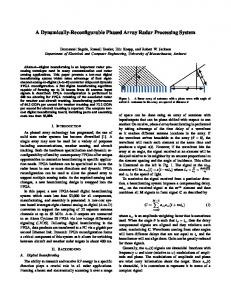
DISTRIBUTED ARRAY RADAR DESIGN AND ANALYSIS T/R MODULE ANALYSIS
Figure 13 shows the block diagram of the T/R module built.. AMP1 LPA-4-14 G =18dB OP1dB =+20dBm
-7 dBm J1
J7
IP
IN
J2
QP
J3
VOUT
CABLE
IN
CBL1
IN
IL =0.2dB
AD 8346 QP
+12V
IP
OUT GND
C1
CABLE CBL2
IL =0.2dB
-8 dBm J5
J4
QN
LO
QN
J6
CABLE
PWUP
-4 dBm LO
PDV1 40266 IL = 3.5 dB
CBL3
IL =0.2dB
CIR1 2 D3C2040 IL =0.5 dB Isolation= 20.5dB 1
J18
CABLE CBL5
3
RFOUT +10 dBm J19
IL =0.2dB
CABLE
+12V GND +5V
IOPP
GND
VS
IOPP
-8 dBm J15
LO
J9
IOPN
IL =0.2dB
J16
J17
C2 J8
CBL4
IOPN
AD 8347 QOPP
+12V
QOPN
J10
J14
RFIP
J11
CABLE
QOPN
GND
QOPP
OUT
CBL6
VGIN J12
IL =0.2dB
IN
CABLE CBL7
AMP2 LNA-2700 G =24dB NF =2 dB
IL =0.2dB
VGIN
Figure 13. 1.
Block diagram of T/R module
Receiver Noise Figure, Effective Temperature and Noise Floor
To calculate the noise figure of the T/R module, consider the receive chain. The noise figure of the T/R module is given by
F = F1 +
F2 − 1 F3 − 1 F4 − 1 + + G1 G1G2 G1G2G3 21
(7)
where F1 =
1 = insertion loss of circulator and cable assembly 7 = 0.9 dB, G1
F2 = noise figure of LNA = 2 dB, G2 = gain of LNA = 24 dB,
F3 =
1 = insertion loss of cable assembly 6 = 0.4 dB, and G3
F4 = noise figure of AD8347 demodulator = 11.7 dB (from [17]).
Thus, Equation (7) gives F = 3.06 dB. The receiver effective temperature Te is given by Te =(F − 1)To .
(8)
Thus, Te ≈ 297 K, assuming To = 290 K. The noise power at the T/R module input is given by N o = k BTe B
(9)
where k B = Boltzmann’s constant = 1.38 × 10⁻²³ J/K, and B = receiver noise bandwidth = 50 MHz. Thus, Equation (9) gives N o ≈ − 96.9 dBm. 2.
Sensitivity and Dynamic Range
The maximum RF power that can be input to the T/R module without it being saturated is limited by the demodulator’s input 1 dB compression point (IP1dB). From [17], the demodulator’s IP1dB ≈ − 22 dBm with no Automatic Gain Control (AGC). Hence, with reference to Figure 13, the maximum RF power that can be input to the T/R module is Prmax = − 22.0 + 0.4 – 24.0 + 0.4 + 0.5 = − 44.7 dBm.
The SNR measured at the T/R module input in this case is
22
⎛ S ⎞ ⎜ ⎟ = − 44.7 – ( − 96.9) = 52.2 dB. ⎝ N o ⎠ max
The minimum RF power that can be input to the T/R module and still be detected depends on the demodulator’s sensitivity. From [17], the demodulator mixer output voltage is linear with RF input power from − 65 dBm to − 5 dBm. Hence, with reference to Figure 13, the minimum RF power that T/R module can effectively receive is Prmin = − 65.0 + 0.4 – 24 + 0.4 + 0.5 = − 87.7 dBm.
⎛ S ⎞ The SNR in this case is ⎜ ⎟ = − 87.7 – ( − 96.9) = 9.2 dB. Thus, the dynamic range N o ⎝ ⎠ min
of the T/R module is − 44.7 – ( − 87.7) = 43 dB. 3.
Maximum Power Output of T/R Module
Burgstaller [2] established the maximum RF power that can be output from the modulator board at 2.4 GHz was about − 6 dBm. Thus, looking at the transmit chain in Figure 13, the maximum RF power output of the T/R module will be Pomax = − 6.0 − 0.4 + 18 − 0.4 − 0.5 = +10.7 dBm.
B.
DISTRIBUTED ARRAY RADAR ANALYSIS
Consider the distributed array radar block diagram in Figure 14 where Ro = reference range from the origin to the target, Rn = range for the nth element which is transmitting, Rm = range for the mth element which is receiving, Pt n = transmitted power at nth element, Pr m = received power at mth element, Go n = gain of antenna of nth element, Go m = gain of antenna of mth element, and
σ mn = target bistatic radar cross section (RCS).
23
Ptn
Transmit Element n
Gon
T/R Module Rn
Prn N transmit elements
σ mn
x
Ro z y
Target Rm
Pt m
Receive Element m
Gom
T/R Module
Prm M receive elements
Figure 14.
Distributed array radar (After [10])
At any one time, N elements may be transmitting and M elements receiving. Normally, all elements would both transmit and receive as well. In such a case, N = M = total number of elements in the array. 1.
System Noise Temperature and Noise Factor
The system noise temperature per channel is given by Ts =Te +Ta
(10)
where Te = receiver noise temperature = 297 K, and Ta = antenna temperature = 300 K. Hence, Equation (10) gives Ts = 597 K. The noise factor per channel is thus N o = 10log( k BTs B ) = − 93.9 dBm.
24
2.
Radar Range Equation
From Figure 14, the total scattered electric field from the target received at element m is N
s Ems = ∑ Emn
(11)
n =1
s where Emn is the root-mean-squared scattered field strength from the target at receive
element m due to transmit element n. It is assumed that the superposition principle applies, i.e., the total electric field at a point is the sum of the individual electric fields from other sources. Assuming that the target is in the far field of the element, the incident power density at the target when element n is transmitting is given by Wni =
Ptn Gon
4π Rn2
.
(12)
The scattered power density returned to the receive element m is thus s Wmn =
Wniσ mn 2 4π Rm
=
Ptn Gon σ mn
( 4π ) Rn2 Rm2 2
(13)
where σ mn is the bistatic RCS and is shorthand notation for σ (θ m ,θ n ) where θ n denotes the incidence aspect angle and θ m the scattered aspect angle. The peak power density is related to the electric field by s Wmn =
s Emn
η
2
=
Ptn Gon σ mn
( 4π ) Rn2 Rm2 2
.
(14)
For free space, η = ηo , so the magnitude of the scattered electric field at receive element m is s = Emn
ηo Ptn Gon σ mn
( 4π ) Rn2 Rm2 2
.
(15)
The phase of the electric field at receive element m is determined by the path lengths (Rn + Rm) and any phase shift introduced by the target echo ( Φσ mn ). Therefore,
25
ηo Ptn Gon σ mn
s = Emn
where k =
2π
λ
( 4π )
2
2 Rn2 Rm
{
}
exp j ⎡⎣ − k ( Rn + Rm ) + Φσ mn ⎤⎦
(16)
.
Applying the superposition principle, the total scattered electric field received at element m from N transmitting elements is given by N
ηo Ptn Gon σ mn
n =1
( 4π )2 Rn2 Rm2
s = ∑ Em
{
}
exp j ⎡⎣ − k ( Rn + Rm ) + Φσ mn ⎤⎦ .
(17)
The received power is related to the electric field by
Prm =
s Em
ηo
2
Ae N Aem = m ∑
ηo
n =1
ηo Ptn Gon σ mn
( 4π )2 Rn2 Rm2
{
}
exp j ⎡⎣ − k ( Rn + Rm ) + Φσ mn + ψ mn ⎤⎦
2
. (18)
where ψ mn accounts for any phase difference in the transmitted and received signals between elements m and n, as well as phase shifts added to focus and scan the beam. The beam scanning phases can be added by the transmit element n or by the receive element at m, or both. Aem is the effective antenna area of receive element m. Finally, using the following relation between gain and effective antenna area [18] Aem =
Gom λ 2
(19)
4π
and substituting it into Equation (18), the total power received by element m is Gom λ 2 N Ptn Gon σ mn exp j ⎡⎣ − k ( Rn + Rm ) + Φσ mn + ψ mn ⎤⎦ Prm = ∑ 3 R R n m ( 4π ) n =1
{
}
2
.
(20)
This is the most general form of the radar range equation for a distributed array radar. For the conventional array with identical elements, equal transmit powers, and phase focusing to achieve coherence at the target,
26
Gom = Gon ≡ Go Ptm = Ptn ≡ Pt
Rn = Rm ≡ Ro σ mn = σ o ψ mn = k ( Rm + Rm ) ≡ 2kRo
Substituting all these quantities into Equation (20) gives 2 NPt )( NGo ) Goσ o λ 2 ( Pt Go2σλ 2 N . Prm = ∑ (1) = ( 4π )3 Ro4 n =1 ( 4π )3 Ro4
(21)
This result is consistent with the radar range equation in [18]. For a conventional N-element array, the total array transmit power is NPt and the array antenna gain is NGo . 3.
Signal-to-Noise Ratio and Detection Range
The SNR at element m for a focused calibrated array operating in a monostatic mode is given by
Ptn Gon σ mn N Prm Gom λ 2 ⎛ S ⎞ exp j ⎡⎣ −k ( Rn + Rm ) ⎤⎦ = = ∑ ⎜ ⎟ 3 Rn Rm ⎝ N o ⎠m N o ( 4π ) k BTs B n =1
{
}
2
.
(22)
For M receive elements in an array, if the radar uses coherent averaging of the returns from each element m, this process involves adding the amplitude of M signals from a target that have coherent phase. The associated power of coherent summation is proportional to M2. Noise is usually assumed uncorrelated Gaussian white noise of random amplitude and phase. The noise power of M signals add to give the noise power of a single signal times M. The signal voltage adds (a factor of M2 in power) and thus, the improvement in SNR is a factor of M. Therefore, the SNR of an array is given by ⎛ S ⎞ ⎛ S ⎞ =M⎜ ⎜ ⎟ ⎟ . ⎝ N o ⎠array ⎝ No ⎠m
(23)
To determine the detection range possible with an eight-element array, the following are assumed: Gom = Gon = 6.6 dB ≡ 4.57,
27
Ptm = Ptn = 10 dBm = 0.01 W,
Rn = Rm = R, σ mn = 0.5 m2, N = M = 8, λ = 0.125 m at 2.4 GHz, Ts = 597 K, and ⎛ S ⎞ ⎜ ⎟ = 9.2 dB ≡ 8.32. ⎝ N o ⎠m The detection range R can be found from Equation (22) to be 62.6 m. The short range is a consequence of operating in the unlicensed Industrial, Scientific and Medical (ISM) band which restricts the power that can be radiated. 4.
Waveform, Sampling Rate and Data Rate
A radar waveform is crucial in target detection, resolution, and range and Doppler ambiguities. If the waveform is Continuous Wave (CW), then its peak power Pt and frequency modulation will affect the radar performance. If the waveform is pulsed, then its properties such as (1) average power Pavg , (2) PRF f p , (3) pulse width τ , and (4) frequency modulation or pulse compression will be the affecting factors. In target detection, if the receiver is designed as a matched filter, the signal-tonoise ratio, according to [19], is given by E S = o N o′ k BTe
(24)
where Eo is the energy of the received target echo and N o′ is the noise power per unit bandwidth. For a pulsed radar, Eo = Ptτ . Thus, in order to detect a target at long distances,
τ needs to be large enough so that there is sufficient energy returned from the target. In terms of resolution, for a pulsed radar, the range resolution is determined by cτ . (25) 2 Thus, the shorter τ is, the better the radar will be in resolving two targets separated in ΔR =
distance. 28
If the receiver bandwidth B is 50 MHz as assumed earlier, then for matched filter response, Bτ ≈ 1 should be observed. This would give a τ of about 20 ns. This may not be achievable with the current National Instruments hardware, as the resolution is about 25 ns from the FPGA clock rate of 40 MHz. This resolution also implies that the range resolution is at best 3.75 m, from Equation (25). While this should not be a problem for the eight-element array, the full-scale array is likely to require better range resolution and so a higher performance solution will need to be sought for. The PRF of a pulsed radar is important in determining the extent that the radar suffers from range and Doppler ambiguities. The higher the PRF of the waveform, the more range ambiguous the radar will be and the lower the PRF, the more Doppler ambiguous the radar will be. The maximum unambiguous range is given by Run =
c . 2 fp
(26)
For a pulsed radar, peak transmitted power is related to the average power by Pt =
Pavg
τ fp
. Assuming the same pulse waveform characteristics for each element m, the
single-pulsed SNR for an element m in the distributed array then becomes N Gon σ mn Pavg Gom λ 2 ⎛ S ⎞ exp j ⎡⎣ − k ( Rn + Rm ) ⎤⎦ ∑ ⎜ ⎟ = 3 ⎝ N o ⎠1 ( 4π ) k BTs Bτ f p n =1 Rn Rm
{
}
2
.
(27)
For Np pulses, assuming coherent integration, the SNR per element will be improved by Np [19]. The SNR of an array of M elements operating in pulsed mode will then be N Gon σ mn Pavg Gom λ 2 ⎛ S ⎞ exp j ⎡⎣ − k ( Rn + Rm ) ⎤⎦ ∑ ⎜ ⎟ = MN p ⎝ No ⎠M ( 4π )3 k BTs Bτ f p n =1 Rn Rm
{
}
2
.
(28)
The sampling rates of the DAC in the NI-9263 Analog Output module and the ADC in the NI-9215 Analog Input module are both 100 kS/s. From discussions with NI application engineers, the maximum frequency of a periodic analog signal that can be generated or detected is recommended to be a factor of 10 below that, meaning 10 kHz. From Equation (26), this implies an unambiguous range of 15 km. While this is good enough for the eight-element array, the full-scale array will have to operate at a PRF of 29
150 Hz or less to achieve an unambiguous detection range of 1000 km or more. At such a low PRF, in order to transmit with the same energy to achieve the SNR at the required detection range, either the peak power of the transmitter or the pulse width has to be increased. The first option may not be favorable as it brings about bulkier devices and heat handling issues, while the second option results in a tradeoff in the minimum range of the radar, as a wider pulse width τ means the receiver is turned on at a later time than before. From [19], sampling loss occurs when the video signal is sampled and digitized by the ADC. This is the difference between the sampled value and the maximum pulse amplitude. For probabilities of detection of 0.90 and false alarm of 10-6, Skolnik [19] states that the sampling loss is 2 dB if sampling once per pulse width and 0.5 dB for two samples per pulse and 0.2 dB for three samples per pulse. The number of samples per pulse Ns is related to the sampling rate fsampling , duty cycle DU and PRF f p by N s = fsampling × DU ×
1 . fp
(29)
Thus, with a sampling rate of 100 kS/s, to keep the sampling loss low with at least three samples per pulse, the ratio of DU to f p , which is τ , should not be lower than 3 × 10⁻⁵ s. A PRF of 1 kHz and 10% duty cycle, which is used in the testing of the T/R module in Chapter V, gives 100 × 103 × 0.10 ×
1 1 × 103
= 10 samples per pulse.
For the array’s data rate requirement, while [9] had identified a total of eight bits for waveform control, phase weighting and phase synchronization commands, the data rate the array has to handle will be dominated by the high resolution of the ADC or DAC. In the demonstrator described in Chapter IV, the National Instruments’ NI-9263 module has a four-channel DAC while the NI-9215 module has a four-channel ADC, each sampling simultaneously at 100 kS/s with a resolution of 16 bits. As each T/R module has one NI-9263 and one NI-9215, the bit rate per element, therefore, is expected to be 100 × 103 × 16 × 8 = 12.8 Mbps. For an eight-element array, the central beamformer and controller needs to handle a total data rate of 8 × 12.8 Mbps = 102.4 Mbps. Hence, a solution proposed by [9] to use commercially available IEEE 802.11g standard or “Wi30
Fi” wireless access points may not be possible as they only support data rates up to 54 Mbps. Demonstration of the wireless communication and synchronization may have to be done on a smaller array, e.g. a four-element array, which requires a data rate of 51.2 Mbps. Other options include selective scheduling of the transmit and receive data exchange so that both processes do not occur simultaneously, or reducing the amount of data that needs to be sent by local processing at the controller in the T/R module. The dynamic range, in dB, of an ADC is given by 20log( 2 N b − 1 ) where Nb is the number of bits of the ADC [20]. Thus, for the NI-9263 and NI-9215, the dynamic range is 96.3 dB. This is well above that of the T/R module whose dynamic range is 43 dB as determined earlier. 5.
Digital Beamformer (DBF) Performance
As mentioned in Chapter II, a generic DBF is made up of an array of (1) antenna elements, (2) T/R modules, (3) ADC and DACs, (4) a digital beamformer, (5) a controller which is a programmable processor with software-coded algorithms, and (6) a calibration unit which matches all the channels to achieve low sidelobes. The digital beamformer usually takes the form of a very fast parallel processor capable of billions of operations per second. It forms multiple beams by finding the inner product of the set of received signal samples (in the example of DBF for receive) and the sets of weights generated by the controller. These weights are calculated in the controller based on the required scan direction needed. The computational load depends on the control algorithm implemented. According to [21], the following parameters are important for a digital beamformer: •
Dynamic Range (DR),
•
Instantaneous bandwidth B, and
•
Number of complex operations per second (COPS) performed by the DBF.
The DR of a digital beamformer depends on (1) the number of bits in the ADC Nb, (2) the number of parallel elements Ne, and (3) the quantization noise. The DR is given by 6Nb + 10logNe. Thus, for the eight-element array prototype using the 16-bits resolution ADCs, Nb = 16 and Ne = 8, the expected DR of the (receive) digital beamformer is 105.0 dB. 31
From Equation (5), the instantaneous bandwidth for the digital beamformer for the eight-element array is calculated to be about 90 MHz. This result is based on a maximum scan direction θ s of 45 degrees and array length D of 0.455 m (eight elements with an inter-spacing of 65 mm). This should be well above what is needed for laboratory testing purpose where the waveforms are relatively simple (CW, pulsed CW or linear frequency modulated). In addition, if the wireless communication and synchronization is carried out with the Wi-Fi devices, their bandwidths are limited to about 20 MHz. The number of COPS a DBF must handle is given by NeB. Thus, with B = 50 MHz and Ne= 8 for an eight-element array, the DSP in the DBF must achieve a computational power of 8 × 50 × 106 = 400 million COPS. 6.
Transmitter Leakage
Transmitter leakage refers to the signal that travels directly from the transmit channel to the receive channel. It needs to be addressed as it concerns the choice of CW or pulsed waveform operating parameter. Figure 15 shows the block diagram of the front end of a typical radar. During transmission, the radar signal travels through the circulator and to the antenna before it is being radiated. Upon hitting a target far away, the target echo is now received by the antenna and is relayed to the receiver (Path 1a-1b). Mathematically, using the notation described in [19], the time-delayed complex signal representation of the target return can be expressed as S1 = A S32 S13 p(t − 2TR ) exp ⎡⎣ j ( 2π ft − 2kR + Φ32 + Φ13 + Φ ant ) ⎤⎦
(30a)
where
A = amplitude factor that combines the effect of antenna gain, path loss to and from the target, target RCS fluctuations, etc., S32 = the low-loss amplitude response from port 2 to 3 of the circulator, S13 = the low-loss amplitude response from port 3 to 1 of the circulator,
TR = the time delay to the target, R = the distance to the target, Φ32 = the phase shift from port 2 to 3 of the circulator,
32
Φ13 = the phase shift from port 3 to 1 of he circulator, and Φ ant = the phase shift contributed by the antenna.
R
p(t) 2a
1a
1b 2b
3a
Figure 15.
3b
Target return vs. reflected and reverse leakage (After [2])
However, this desired echo which contains amplitude and phase information about the target, has to compete with two other signals. The first one, denoted by Path 2a2b, is the part of the transmitted radar signal which travels through port 2 to 3 of the circulator but is reflected due to the antenna mismatch back towards port 1 of the circulator at the receive end. The complex signal representation of the antenna mismatch component can be expressed as
S2 = S32 S13 Γ ant p (t − T2 ) exp ⎡⎣ j ( 2π ft − kR2 + Φ 32 + Φ13 + Φ′ant ) ⎤⎦
(30b)
where Γant = the magnitude of the reflection coefficient of the antenna,
T2 = the time delay through path 2, R2 = length of path 2, and Φ′ant = the phase of the reflection coefficient of the antenna. The other signal, denoted by Path 3a-3b, is the transmitter leakage which travels directly from port 2 to port 1 of the circulator and to the receiver. The complex signal representation of the reverse leakage can be expressed as
S3 = S21 p(t − T3 ) exp ⎡⎣ j ( 2π ft − kR3 + Φ 21 ) ⎤⎦ 33
(30c)
where S21 = the reverse isolation from port 2 to 1 of the circulator,
T3 = the time delay through path 3, R3 = length of path 3, and Φ 21 = the phase shift from port 2 to 1 of the circulator. To assess the impacts of S2 and S3, the following component data were extracted from the measurements done by Burgstaller [2] (the phase data have been ignored for simplicity): S32 = 0.447 dB loss ≡ 0.902, S13 = 0.448 dB loss ≡ 0.902, S21 = 19.73 dB isolation ≡ 0.0106, and Γant = 0.18.
If the original transmitted signal p(t) is normalized with unit magnitude and zero phase shift, then the following results are obtained: S1 = A(0.902)2 = 0.814A. S 2 = (0.18)(0.902)2 = 0.146. S3 = 0.0106.
To calculate A, which is the amplitude loss factor due to the antenna gain, twoway path loss, target RCS fluctuations etc, the simplified radar range equation in [19] can be applied:
P G G σλ 2 Pr = t t r ( 4π )3 R 4 where Pt = peak power transmitted,
Pr = power received at the antenna, Gt = gain of transmit antenna = 6.6 dB ≡ 4.57, Gr = gain of receive antenna = 6.6 dB ≡ 4.57, 34
(31)
σ = 0.5 m2,
λ = 0.125 m, and R = 62.6 m. P Thus, A2 = r = 5.35 × 10⁻¹² from Equation (31). Hence, A = 2.31× 10⁻⁶. Pt The above result shows the antenna mismatch component will be dominant if the receiver is on during transmission. In addition, the ratio of the unwanted signals to the wanted target return,
S + S3 S 2 + S3 , can be simplified to 2 . This gives a ratio of 83,283 S1 S1
or 49.2 dB. If the target return needs to be 10 dB higher than the mismatch and reverse leakages, then the latter need to be suppressed by almost 60 dB. Several approaches to solve this problem are described in greater detail in Chapter VI. As a summary, this chapter has analyzed some of the key T/R module parameters such as noise figure, sensitivity, maximum output power, etc. They are tabulated in Table 1. On the distributed array system level, the SNR of a single element and the array as a whole were derived, the results of which were consistent with the standard radar range equation. In addition, key parameters, such as waveform, digital beamformer performance, sampling rate and data rate requirements, were analyzed for an eightelement array. The results are summarized in Table 2.
Parameter Bandwidth Noise output power Noise figure Noise temperature Max. RF input power Sensitivity Dynamic range Max. RF output power
Table 1.
Performance 50 MHz − 96.9 dBm 3.06 dB 297 K − 44.7 dBm giving SNR of 52.2 dB − 87.7 dBm giving SNR of 9.2 dB 43 dB +10.7 dBm
Summary of performance analysis of the T/R module
35
Parameter Bandwidth
Noise output power Noise temperature Detection range PRF and Duty cycle
Performance/Requirements 50 MHz (may be limited to 20 MHz if using Wi-Fi devices) − 93.7 dBm 597 K 62.6 m DU or τ above 3x10⁻⁵ s Keep fp
to maintain at least 3 samples per pulse Data rate 102.4 Mbps Computational power of DBF 400 million COPS Table 2.
Summary of performance/requirement analysis of an eight-element array
36
IV. A.
HARDWARE AND SOFTWARE DEVELOPMENT
ELECTRICAL DESIGN OF T/R MODULE
This section describes the details of the electrical design of the prototype T/R module. Figure 16 shows the block diagram schematic. Burgstaller [2] has done a thorough characterization of the various components such as the circulator, low noise amplifier, low power amplifier, AD8346 modulator evaluation board and AD8347 demodulator evaluation board. The remaining items to characterize are the interconnecting RF cable assemblies and the 1:2 power splitter used to split the incoming LO into two equal signals, one for the modulator board and the other for the demodulator board. All the components are then integrated into a chassis to form a complete T/R module. For the purpose of testing, the baseband I and Q data signals are still hardwired to the various components. A component list is given in Table 3.
Figure 16.
Schematic of T/R module 37
S/N
Designation
Part Number
Manufacturer
1
C1
AD8346 EVAL
Analog Devices
2
C2
AD8347 EVAL
Analog Devices
3
AMP1
LPA-4-14
RF Bay Inc
4
AMP2
LNA-2700
RF Bay Inc
5
PDV1
40266
Anaren
6
CIR1
D3C2040
DITOM Microwave Inc
Table 3. 1.
RF component list of T/R module
Power Divider
The power divider from Anaren, part no. 40266 [22] operates in the frequency range 2 to 4 GHz. Table 4 gives a summary of the parameters of the device. The amplitude and phase balance plots are given in Figures 17 and 18 respectively. S/N
Parameter
Result (at 2.4 GHz)
1
Input port VSWR
1.07
2
Output port 1 VSWR
1.07
3
Output port 2 VSWR
1.05
4
Insertion loss S31
-3.04 dB
5
Insertion loss S21
-3.07 dB
6
Amplitude balance
0.02 dB
7
Phase balance
0.76 deg
Table 4.
Summary of performance of power divider
38
Figure 17.
Figure 18. 2.
Amplitude balance of power divider
Phase balance of power divider
RF Cable Assemblies
The interconnecting RF cables are self-assembled using the various jigs provided by the Microwave Laboratory. The connector at each end can be either a SMA male straight plug (part no. 901-9501-3 [23]) or a right angled connector (part no. 901-9521-3 [23]) from Amphenol. The RF cable type is RG-316. Figure 19 shows a typical S21 insertion loss and phase measurements on one such RF cable assembly. The average insertion loss is about 0.4 dB at 2.4 GHz. Table 5 gives the detailed RF cable assembly definitions. 39
Insertion loss
Phase
Figure 19.
Cable Assy No. 1
In
Out
From
To
Length (mm)
SMA-M right angle
SMA-M straight
Modulator Vout
AMP1 In
140
2
SMA-M straight
SMA-M right angle
AMP1 Out
CIR1 Port 2
170
3
SMA-M right angle
SMA-M right angle
PDV1 Output 1
Modulator LO
180
4
SMA-M right angle
SMA-M right angle
PDV1 Output 2
Demodulator LO
180
5
SMA-M right angle
SMA-M right angle
T/R module LO port
PDV1 Input
120
6
SMA-M straight
SMA-M right angle
AMP2 Output
Demodulator RFIP
150
Table 5. 3.
Insertion loss and phase measurements of RF cable assembly
Definition of RF cable assemblies used in T/R module
Optimum AD8346 and AD8347 Settings
Burgstaller [2] investigated the performance of the AD8346 and AD8347 boards and concluded the following:
40
i.
The modulator differential control signals should be DC-biased to approximately 1.2 V. That means, the differential I/Q channel baseband inputs should be calculated using the following relations: 1 IP(θ ) = 1.2 + I (θ ) 2 1 IN (θ ) = 1.2 − I (θ ) 2 1 QP(θ ) = 1.2 + Q (θ ) 2 1 QN (θ ) = 1.2 − Q(θ ) 2
(32)
where I (θ ) and Q (θ ) were defined in Equation (6). ii.
VGIN to the AD8347 should be set to about 0.38 V to provide the largest I-Q circle without distorting the differential outputs.
B.
MECHANICAL DESIGN OF T/R MODULE
This section describes the mechanical design of the T/R module. The mechanical chassis is a 8 inch by 4 inch by 2 inch aluminum box from Digi-Key. All the components selected were then integrated into the chassis as shown in Figure 20. LO port
DC power and I-Q data lines
RF port
Figure 20.
Assembled T/R module
41
Note that in order to provide minimum stress to the RF connectors, most of the cable assemblies are longer than the shortest length so as to provide some flex. The LNA and LPA are as closely mounted to the wall as possible so that there is adequate heat dissipation. The pins of the AD8346 EVAL board are separated from those on the AD8347 EVAL board by spacers. All the I and Q data lines and DC power lines go in and out of the T/R module from the back end. Table 6 gives the screw definition.
S/N
Designation
Component
Screw type
Qty
Remarks
1
C1
AD8346
#4-40
4
With nuts
2
C2
AD8347
#4-40
4
With nuts
3
AMP1
LPA 4-14
#4-40
4
4
AMP2
LNA-2700
#4-40
4
5
CIR1
D3C2040
#2-56
3
6
PDV1
40266
#4-40
2
Table 6. C.
With nuts
Definition of screws used in T/R module
CONTROLLER AND DATA ACQUISITION SYSTEM 1.
cRIO Embedded System
The hardware for controlling the TR module for performing signal processing and digital beamforming is provided by National Instruments’ Compact Reconfigurable Input Output (cRIO) modules. The cRIO Embedded System consists of C series I/O modules, a Reconfigurable Chassis containing the FPGA and a Real-Time Controller capable of performing deterministic floating point calculations. Figure 21 shows the hardware which will be described in more detail in the following sections.
Figure 21.
cRIO modules (From [2]) 42
2.
cRIO Reconfigurable Chassis and Controller
The NI-9104 eight-slot Reconfigurable Chassis [24] is the heart of the cRIO system because it contains the reconfigurable I/O core. The RIO FPGA core, which has an individual connection to each I/O module, is programmed with elemental I/O functions to read or write signal information from each module. Because there is no shared communication bus between the RIO FPGA core and the I/O modules, I/O operations can be precisely synchronized to 25 ns resolution, with the hardware clock rate at 40 MHz [24]. The RIO core is connected to the cRIO Real-Time Controller cRIO-9004 through a Personal Communications Interface (PCI) bus interface. The cRIO-9004 [25] has 64 MB of Dynamic Random Access Memory (DRAM) memory and 512 MB of non-volatile flash storage for data logging applications. Typical functions include retrieving data from any control or indicator on the front panel of the FPGA application and performing single point control, waveform analysis, data logging and Ethernet or serial communications. The LabVIEW FPGA module is used to program the FPGA on the cRIO reconfigurable chassis and includes powerful, ready to use, fixed-point functions to process signals directly on the FPGA. It was reported in [26] that large waveforms with up to 8192 16-bit samples can be loaded to the FPGA core, thus allowing for high resolution waveforms. 3.
NI-9263 Analog Output Module
The NI-9263 Analog Output (AO) Module [27] is an industrial-grade module which connects directly to the RIO FPGA core and can output the required voltage waveform to the external device. It has 4 channels per module, but each channel has its own DAC allowing for simultaneous analog output. The resolution is 16-bit and the simultaneous update rate is 100 kS/s per channel. 4.
NI-9215 Analog Input Module
The NI-9215 Analog Input (AI) Module [28] is an industrial-grade module which connects directly to the RIO FPGA core and acquires the signals, performs signal conditioning and communicates the digital signals to the FPGA. It has 4 channels per module, each channel having 16-bit resolution and a 100 kS/s simultaneous update rate. 43
5.
Software Model
Figure 22 shows the software model. In the test bench set up, the host computer acts as the digital beamformer and controller. It runs the Microsoft Windows Operating System as well as National Instruments’ application software LabVIEW. The latter will enable the user to program Virtual Instruments (VIs) which will enable the host computer to transfer commands and data to and from the FPGA hardware in the digital T/R module. Thus, a FPGA interface VI is created in the host computer and a FPGA VI created and downloaded to the FPGA hardware.
Figure 22. 6.
Software model (From [2])
Arbitrary Waveform Generation
Some effort was made in evaluating an arbitrary waveform generator example program given in [26]. Using the FPGA module, the program was able to help the hardware perform the following functions: •
Write data to the FPGA memory,
•
Read data from the FPGA memory,
•
Output the data to an analog output channel (the NI-9263 for example), and
•
Allow the user to adjust the waveform frequency and amplitude while the signal is continuously output.
For the program to work, the user has to have the data written in a specific format and saved as a LabVIEW Measurement file which the example program can call. Alternatively, NI has an Analog/ Digital Waveform Editor software which helps the user to create arbitrary waveforms more easily with its interactive tools. The waveforms can be saved in a binary or ASCII format which the Read File routine will be able to access. 44
While some time and effort need to be invested in troubleshooting the example program, this arbitrary waveform generation function could be built into the array demonstrator in future so that there is a DDS capability which allows for more complex waveforms like pulse compression or chirp waveforms to be experimented with. D.
TWO-ELEMENT ARRAY DEMONSTRATOR TEST BENCH
The proposed test bench is shown in Figure 23. An external LO source [29] provides a signal at frequency 2.4 GHz and power of about +3 dBm. A two-way power divider splits the LO signal into two equal signals, each fed to the LO port of the two T/R modules. A 3 dB attenuator is placed at each LO port so that the final LO power reaching the AD8346 and AD8347 boards is about − 8 dBm as recommended by the manufacturer [30, 17]. For each T/R module, the IP, IN, QP and QN signals from the AD8346 modulator board are connected to the NI-9263 AO output terminals. The IOPP, IOPN, QOPP, QOPN signals from the AD8347 demodulator board are connected to the NI-9215 AI input terminals. The host computer connects to the NI cRIO-9004 controller via a Ethernet connection. The power to the cRIO-9004 and cRIO-9104 FPGA is from a power supply adapter connected to the mains. The required voltages of +5V, +12V, VGIN (+0.38V) come from standard COTS benchtop power supply units. Figure 24 shows the actual test bench built.
45
Figure 23.
Host computer
Block diagram of two-element array demonstrator test bench
+VGIN power supply
+12V power supply
+5V power supply VCO
LO ports
cRIO-9004 and 9104
NI-9263 Figure 24.
NI-9215
Two-element array demonstrator test bench 46
E.
LABVIEW PROGRAM
In using LabVIEW and the Compact RIO embedded system, there are three main steps to developing a working program: •
Define the various hardware to use with the FPGA module.
•
Develop the FPGA application. This allows the FPGA to interact with the AO and AI modules. The format of the FPGA VI typically consists of a three-frame flat sequence structure which performs (a) timing and triggering, (b) control and module I/O and (c) synchronization with the host.
•
Develop the host application. This allows the host to access the FPGA and perform such operations as downloading, reading or writing data, starting or stopping the VI.
1.
LabVIEW Project Structure
The test software for the two-element array demonstrator is in the file Two Element Demonstrator Array.lvproj. The project structure is as shown in Figure 25.
Host VI Set up two NI-9263 AO modules Set up two NI-9215 AI modules
FPGA VI
Figure 25.
LabVIEW project structure
The host VI called Two Element Array(Host).vi, acts as the main program which performs the following tasks: •
runs a calibration routine for the NI-9263 and NI-9215 modules,
•
reads in system control parameters such as amplitude and scan direction of the array, loop rate, duty cycle, frequency and passes them to the FPGA,
•
sends the required I and Q data to the FPGA and out via the NI-9263 AO module to control the modulator phase shift, 47
•
extracts the baseband I and Q data received from FPGA via the NI-9215 AI module and performs signal processing e.g. averaging, calculation of the amplitude and scan direction, etc.
Convert to Binary.vi, which was from NI software library, converts the output
voltage values into binary code representation as the latter is required when performing analog operations with cRIO modules. Convert to Voltage.vi does the reverse, converting binary code representation
back into the analog voltage output values. The VI downloaded to the FPGA target called Two Element Array (FPGA).vi enables the host to read the required data from the desired AI terminal or write data to the desired AO terminal. 2.
User Interface
Figure 26 shows the user interface. Some of the key settings are highlighted. There is a main controls palette. This allows the user to vary the duty cycle, PRF and the number of points per waveform cycle. The loop rate, which controls how fast the data is being read or written to the FPGA, can also be adjusted. There is a palette whereby individual T/R modules can be controlled. If only testing of the transmission is needed, then only the transmit switches for the T/R modules need to be turned on. If only testing of the reception is needed, then only the receive switches for the T/R modules need to be turned on. If both the transmit and receive switches are turned on, the T/R modules will only operate in pulsed mode, i.e. when transmitting, the receive chain is “shut down” and vice versa. If the duty cycle is turned to 100%, then the waveform is CW. For each T/R module, the user can adjust the amplitude and phase by adjusting the Magnitude and Phase dials. The corresponding I and Q data, based on Equations (6) and (32) are displayed as IP, IN, QP and QN. The three charts, from top to bottom, show the real-time analog I and Q data read from the NI-9215 AI module, the 100-point averaged amplitude A(t) and 100-point averaged phase θ(t) of the received signal respectively. The signal is recovered by
48
A(t ) = I 2 (t ) + Q 2 (t ) ⎛ Q (t ) ⎞ ⎟. ⎝ I (t ) ⎠
θ (t ) = tan −1 ⎜
and
(33a) (33b)
Main controls (same for all elements)
Controls for individual T/R module
Figure 26.
Demonstrator user interface
As a summary, this chapter has described the hardware of the T/R module, as well as the NI devices and software used to build the two-element array demonstrator test bench. The next chapter describes the measurements conducted to evaluate the T/R module’s performance.
49
THIS PAGE INTENTIONALLY LEFT BLANK
50
V. A.
MEASUREMENTS AND RESULTS
DC POWER CONSUMPTION
The DC power consumption of the T/R module was measured and is tabulated in Table 7.
S/N
Designation
Component
Voltage (V) Current (mA)
Power (W)
1
C1
AD8346
+5.0
30
0.15
2
C2
AD8347
+5.0
61
0.30
+0.38
0.6 µA
Negligible
3
AMP1
LPA 4-14
+12.0
85
1.02
4
AMP2
LNA-2700
+12.0
55
0.66
Total
2.13
Table 7.
DC power consumption of T/R module
Note that the above measurement excludes the power consumption of the VCO. At +5V, the VCO draws about 58 mA, thus giving a power consumption of 0.29 W.
B.
INTERFERENCE BETWEEN DEMODULATOR BOARDS
THE
MODULATOR
AND
These tests were performed to check if the proximity of the modulator and demodulator boards would cause interference in the signals measured. 1.
Transmit Output when Demodulator is On/Off
From the test setup shown in Figure 27, it can be seen that only T/R module 1 was activated. A CW signal was injected into the receive end at the LNA input while the circulator port to the LNA was terminated with a 50 ohm load. The RF transmit port was connected to a negative polarity HP423B detector and fed to Channel 1 of the oscilloscope. With the CW signal turned off and on, the transmitted output waveform was observed. 51
Figure 27.
Setup for measuring demodulator’s effect on transmitter output
Figure 28 shows the transmit output when the demodulator was off and Figure 29 shows it when the demodulator was on.
Figure 28.
Transmit output when demodulator was off
52
Figure 29.
Transmit output when demodulator was on
There was no noticeable change in the transmit output when the receive end was on or off. 2.
Receive Output When Modulator is On/Off
From the test setup shown in Figure 30, a CW signal was injected into the receive end at the LNA input while the transmit port and circulator receive output were terminated with 50 ohm loads. The transmitter was turned on and off and the receive output was observed in the Element Analog Input Chart in the User Interface. Figures 31 and 32 show the receive output when the transmitter was off and on respectively.
53
Figure 30.
Setup for measuring modulator’s effect on received output
IOPP, IOPN, QOPP, QOPN signals
Figure 31.
Receive output when modulator was off
54
IOPP, IOPN, QOPP, QOPN signals
Figure 32.
Receive output when modulator was on
It can be seen that there were no noticeable changes to the IOPP, IOPN, QOPP, QOPN signals whether the modulator was on or off. The signals remained in the 0.95 to 1.05 V range as before. From the two series of measurements, it can be concluded that the interference between the modulator and demodulator boards is not significant enough to affect the performance of the eight-element array to be built later. C.
TRANSMIT AND RECEIVE DELAYS
Measurements were taken to give an indication of the delays in the transmit and receive paths inside the T/R module. The delay is a measure of the response time of the electronics in the modulator and demodulator as well as propagation delay. The electronics include mixers, filters and baseband amplifiers. The delay is important as it affects the time response of the radar and determines the threshold setting for the time of arrival. The devices used to measure the RF output thus need to have short delay and any residual delay must be compensated for in the range calculation. The HP423B negative polarity RF detector used in this measurement has a 8 to 12 ns rise time [31]. 1.
Transmit Delay
In the setup shown in Figure 33, one of the NI-9623 analog outputs AO0 was connected to Channel 1 of the oscilloscope and set as the trigger source, and the RF 55
transmit output of T/R Module 1 was connected to a HP 423B RF detector and then to Channel 2 of the oscilloscope. This measurement was done in the pulsed mode so that the ON and OFF edges of the signals could be measured. Figures 34 and 35 show the rise and fall response times. The delay was measured from the baseband 50% to the RF 10% or 90% level.
Figure 33.
Setup for measuring transmit delay
AO0 signal OFF to ON
RF signal OFF to ON
Figure 34.
Transmit delay (rising edge)
56
RF signal ON to OFF
AO0 signal ON to OFF
Figure 35.
Transmit delay (falling edge)
The average delay measured was about 2.5 µs. This implies that the radar would have to schedule at least 5 µs in each Pulse Repetition Interval (PRI) to allow for this delay. It is noted that the above measurement was not the measurement of the delay in the T/R module, as the response time of the signal envelopes may be limited by that of the DAC in the NI-9263 Analog Output module. A simple experiment was performed with a high-speed function generator providing the pulsed AO0 signal instead of the DAC. Figures 36 and 37 show the results.
AO0 signal OFF to ON
RF signal OFF to ON
Figure 36.
Transmit delay (rising edge) with function generator 57
RF signal ON to OFF
AO0 signal ON to OFF
Figure 37.
Transmit delay (falling edge) with function generator
It can be seen that there is a 46 ns delay between the start of AO0 signal transition and the start of the RF signal transition from off to on, and a 20 ns delay between the two signals from on to off. These are likely the actual propagation delays in the electronics (modulator, PA and circulator) in the T/R module, discounting the delays in the short interconnecting RF cable assemblies. The modulator and PA are solid-state devices working from 800 to 2500 MHz and DC to 4000 MHz respectively. This implies that their rise and fall times should be on the order of sub-nanoseconds and so the delays measured in Figures 36 and 37 could be attributed to the circulator itself. As the eight-element array prototype is likely to be working with a Pulse Repetition Interval (PRI) on the order of milliseconds and the pulse width a fraction of that, i.e. hundreds of microseconds, the delays measured in this section and those which follow are not very critical and hence are measured using the DAC or ADC in the NI9263 or 9215 module respectively. Further investigation may be done to ascertain if the response times of the DAC or ADC can be improved. 2.
Receive Delay
In the setup shown in Figure 38, the pulsed RF transmit output from T/R Module 2 was divided by a 1:2 power splitter into two equal signals, one of which was connected to the RF detector and to Channel 1 of the oscilloscope and set as the trigger source, 58
while the other was injected into the RF port of T/R Module 1. The NI-9215 analog input AI0 line was tapped to Channel 2 of the oscilloscope. Figure 39 shows the receive delay for the rise edge.
Figure 38.
Setup for measuring receive delay
RF signal ON to OFF
AI0 signal ON to off
Figure 39.
Receive delay (rising edge)
59
The average receive delay was about 2 µs. Again, it is noted that the measurement above reflected the response time of the DAC, which affected the rise time of the RF, pulsed signal from T/R module 2. D.
SIMULTANEOUS TRANSMISSION AND RECEPTION
Measurements were done to ascertain if the LabVIEW code has been correctly implemented in the FPGA and to demonstrate that two T/R modules can transmit and receive simultaneously. 1.
Simultaneous Transmission
In the setup shown in Figure 40, the RF transmit outputs of two T/R modules were connected to HP 423B RF detectors and then to Channels 1 and 2 of the oscilloscope respectively. Figures 41 and 42 show the time difference between the transmitted signals from the two T/R modules. The average time difference, from 10% to 90% level of the signals, was about 3 μs. Oscilloscope cRIO-9104 Reconfigurable Chassis NI9263 NI9215
Ch1 Ch2
RX OFF
I
Mod Q LO IO
RF detector
Demod QO
T/R Module 1
I
NI9263
Mod Q LO IO
NI9215
Ethernet
Demod QO
T/R Module 2
RX OFF
RF detector
cRIO-9004 real-time controller
Host computer
Figure 40.
Setup for testing synchronous transmission
60
RF from T/R module 2 RF from T/R module 1
Figure 41.
Simultaneous transmit off to on
RF from T/R module 1 RF from T/R module 2
Figure 42. 2.
Simultaneous transmit on to off
Simultaneous Reception
In the setup shown in Figure 43, a pulsed RF signal was divided and injected into each of the RF port of T/R modules 1 and 2. The AI0 lines on T/R module 1 and 2 were tapped and connected to Channels 1 and 2 of the oscilloscope respectively. Figure 44 shows the time difference between the received baseband data from the two T/R modules.
61
Figure 43.
Setup for testing synchronous reception AI0 line from T/R module 1 AI0 line from T/R module 2
Figure 44.
Simultaneous receive on to off
62
The time difference was about 1 μs. Hence, the average time difference for transmit and receive was 2 μs. This should not significantly affect the performance of the eight-element array. Again, it is noted that the measurements above included the response time of the DAC or ADC. E.
PHASE ERROR MEASUREMENT
In the setup shown in Figure 45, a CW RF signal was transmitted from T/R module 1 to T/R module 2. The I-Q differential amplitude on T/R module 1 was set to 2 V and the transmitted phase θ t varied from 0 to 360 degrees. The RF signal was passed through a RF attenuator of about 60 dB to bring the input RF power to a level of about − 50 dBm so that it is within the linear operating range of the receive channel. The
received differential pairs of I(t) and Q(t) voltages, and phase θ r were recorded and tabulated in Table 8. A plot of θ r vs. θ t is shown in Figure 46, with a least squares line fit done. cRIO-9104 Reconfigurable Chassis NI9263
I
Mod LO
TX ON
Q IO
NI9215
Demod QO
RF Attenuator
T/R Module 1
I
NI9263
Mod LO
Q IO
NI9215
Ethernet
Demod QO
RX ON
cRIO-9004 real-time controller
VCO
Host computer (run LabVIEW VI)
Figure 45.
T/R Module 2
Setup for phase error measurement
63
Phase Error Measurement
360
Received Phase (deg)
270
180
90
0 0
90
180
270
360
-90 Transmitted Phase (deg)
Figure 46.
Plot of received phase vs. transmitted phase
From Figure 46, the line fit equation is θ r = 0.9952θt − 40.146 . Thus, accounting for an offset of -40 degrees, there is actually very little error between the received and transmitted phases. The maximum phase error is probably about (1 − 0.9952) × 360 = 1.7 degrees. The offset is likely due to the constant phase shift of the attenuator and RF cable connected between T/R modules 1 and 2 and can be removed during calibration of the array. This further shows the transmit and receive paths of the T/R module are functioning as required.
64
θ t (deg) 0 10 20 30 40 50 60 70 80 90 100 110 120 130 140 150 160 170 180 190 200 210 220 230 240 250 260 270 280 290 300 310 320 330 340 350 360
Table 8.
F.
I+ (V) 1.021 1.023 1.025 0.167 1.027 1.028 1.026 1.024 1.023 1.020 1.016 1.012 1.007 1.004 0.999 0.994 0.990 0.987 0.984 0.982 0.979 0.978 0.977 0.977 0.978 0.982 0.982 0.985 0.988 0.994 0.998 1.003 1.007 1.011 1.016 1.019 1.020
I- (V) 1.001 1.001 1.000 0.997 0.998 0.996 0.998 1.000 1.002 1.006 1.009 1.012 1.018 1.021 1.027 1.031 1.035 1.038 1.042 1.044 1.046 1.047 1.048 1.049 1.046 1.044 1.043 1.039 1.037 1.030 1.027 1.022 1.018 1.013 1.009 1.006 1.003
Q+(V) 1.010 1.016 1.020 1.023 1.028 1.032 1.037 1.041 1.045 1.048 1.050 1.052 1.051 1.054 1.053 1.054 1.050 1.047 1.046 1.041 1.037 1.030 1.029 1.025 1.020 1.017 1.013 1.011 1.008 1.007 1.005 1.004 1.005 1.005 1.007 1.009 1.012
Q- (V) 1.010 1.007 1.004 1.000 0.996 0.991 0.987 0.982 0.978 0.976 0.975 0.972 0.972 0.970 0.970 0.971 0.974 0.977 0.978 0.981 0.986 0.989 0.994 0.998 1.002 1.006 1.010 1.013 1.015 1.016 1.018 1.020 1.018 1.018 1.016 1.013 1.011
A r (V) θ r 0.052 0.046 0.046 0.048 0.050 0.052 0.052 0.053 0.053 0.055 0.049 0.052 0.049 0.050 0.052 0.050 0.052 0.049 0.053 0.053 0.050 0.051 0.050 0.050 0.051 0.050 0.048 0.048 0.047 0.005 0.046 0.046 0.047 0.048 0.048 0.047 0.049
(deg) -38.0 -28.2 -18.6 -10.0 0.2 11.4 21.2 32.0 41.8 50.4 59.5 68.0 78.6 89.1 98.9 108.0 118.4 127.9 137.8 146.1 156.5 165.3 175.7 185.1 194.6 205.1 214.5 225.6 234.4 249.0 258.0 270.5 282.4 292.9 303.2 313.5 321.8
Measured received I and Q voltages and phase (with differential input amplitude of 2 V)
S11 OF T/R MODULE RF PORT
Burgstaller [2] measured the S11 of the dipole antenna element to be used in the demonstrator array. As seen from Chapter II, the antenna reflection coefficient is important in (1) determining the leakage between the transmit and receive channels, as well as (2) affecting the array RCS. The S11 of the RF port of the T/R module was 65
measured using a Vector Network Analyzer (VNA). Figure 47 shows that at 2.4 GHz, a return loss of -16.5 dB was obtained, which corresponds to a VSWR of 1.4.
Figure 47.
S11 of RF port of T/R module
As a summary, various power and timing measurements were done on the T/R module. They showed that despite the close proximity of the modulator and demodulator boards in the compact T/R module chassis, there was no significant interference between them. Also, given the NI hardware configuration, the various propagation delays of the transmit and receive paths were acceptable as the PRI of the eight-element array is likely to be in the order of milliseconds and the pulse width a fraction of that, i.e., hundreds of microseconds. The test bench software functioned properly with two T/R modules simultaneously transmitting and receiving on the order of two microseconds on average. In addition, the propagation delays in both the transmit and receive channels of the T/R module are very small that they should not affect the performance of the eight-element array.
66
VI. A.
CONCLUSIONS AND RECOMMENDATIONS
CONCLUSIONS
An analysis of the performance of the T/R module and the requirements for an eight-element distributed array radar were done, the results of which are summarized in Tables 9 and 10, respectively. Parameter Bandwidth Noise output power Noise figure Noise temperature Max. RF input power Sensitivity Dynamic range Max. RF output power
Table 9.
Performance
50 MHz − 96.9 dBm 3.06 dB 297 K − 44.7 dBm giving SNR of 52.2 dB − 87.7 dBm giving SNR of 9.2 dB 43 dB +10.7 dBm Summary for the T/R module
Parameter Bandwidth
Performance/ Requirements 50 MHz (may be limited to 20 MHz if using Wi-Fi devices) − 93.7 dBm 597 K 62.6 m DU Keep or τ above 3x10⁻⁵ s fp
Noise output power Noise temperature Detection range PRF and Duty cycle
to maintain at least 3 samples per pulse Data rate 102.4 Mbps Computational power of DBF 400 million COPS Table 10.
Summary for an eight-element array
A number of characterization measurements were done on the T/R module. These measurements showed the following: •
There was no observable interference between the modulator and demodulator boards inside of the T/R module chassis.
•
The total delays in the transmit and receive paths, including the response time of the electronics and NI hardware, in the T/R module were on the 67
order of five microseconds. The actual delay is likely to be much shorter and will not be a problem with the eight-element array demonstrator which is expected to be working with a PRI of milliseconds and pulse width of hundreds of microseconds. •
Given the existing hardware, two T/R modules could transmit or receive simultaneously within two microseconds on average. Again, the difference could be smaller and is not expected to be a problem for the eight-element array demonstrator.
•
There was good agreement between the received and transmitted phases between two T/R modules, less an offset of 40 degrees which can be attributed to the RF attenuators and cables connected between the two T/R modules. The offsets will be removed during the antenna calibration.
In conclusion, two T/R modules were successfully built and a two-element demonstrator test bench was completed. A test software, written with LabVIEW, has enabled each T/R module to transmit or receive in CW or pulsed mode. The sampling loss is related to the number of samples per pulse which is in turn determined by the sampling rate of the ADC or DAC, duty cycle and PRF of the radar waveform. Given a 100 kS/s sampling rate, it was concluded that the ratio of duty cycle to PRF should be kept above 3 × 10⁻⁵ s so as to have at least three samples per pulse. B.
RECOMMENDATIONS FOR FUTURE WORK
To continue the work to build the prototype eight-element array radar, the following areas need to be studied or worked on: 1.
Expand the Array Demonstrator Test Bench
For the hardware, six more T/R modules need to be assembled and tested. For the test and control software, six similar transmit and receive subroutines need to be added to the host VI (Two Element Array (Host).vi) and the FPGA VI (Two Element Array (FPGA).vi). 2.
Time and Phase Synchronization Method
The key to operating a distributed array radar is achieving two-way coherent operation by means of time and phase synchronization between the array elements. The methods proposed and experimentally proved by Attia [32] should be further studied to assess the additional hardware and software solutions needed to bring time synchronization and phase cohering for the eight-element array.
68
The eight-element array will require the use of two NI cRIO-9104 chassis. The chassis will need to be synchronized. The following methods described in [33] may be considered: •
Use a common hardware trigger which synchronizes events between the systems. This is implementable with digital I/O modules in each system. The master system sends a digital pulse to one of its digital outputs. Each of the slave systems will look for this pulse on one of their digital inputs and start their process,
•
Use a shared clock signal between multiple cRIO systems and use the external clock to run specific processes on each cRIO chassis that needs to be synchronized. In this way, processes will be done at the same rate fully synchronized on multiple systems, or
•
Implement a fully synchronized hardware solution. This needs a digital I/O module in each chassis. The master device generates a digital signal and reads it to each of the slaves.
3.
Transmit Leakage Reduction or Cancellation Method
Because of the short range due to the low power operation, there will be overlap in the transmit and receive pulses unless an ultra-short pulse is used. Direct leakage from the transmitter must be cancelled in order to detect targets with low SNR. Also, using the CW mode results in the presence of the transmitter leakage, described in Chapter II, which the present hardware cannot cancel. If future testing is to be done with CW signals when all the elements are transmitting or receiving simultaneously, then the following leakage reduction or cancellation methods may be studied: •
Reducing leakage by increasing the isolation – a pair of PIN diode switches may need to be included in the transmit and receive chain. One switch is likely to be after the power amplifier before the circulator and the other switch after the circulator before the low noise amplifier. Thus, when transmitting, the PIN diode switch in the transmit chain is on and the switch in receive chain off, thus better isolating the receive chain during transmission. When receiving, the reverse happens with the PIN diode switch in the transmit chain off and the switch in receive chain on. A PIN diode switch can provide 40 to 50 dB isolation and can handle relatively large powers. Its switching speed is in the order of nanoseconds and thus should not affect the radar operation significantly.
•
Reducing leakage by having separate antennas – Another solution may be to have separate transmit and receive antennas on the T/R module, if there is no space constraint. The transmit path would be effectively
69
isolated from the receive path inside the T/R module. Diversity techniques in frequency or space could be used to address the issue of mutual coupling between the closely spaced antennas. This would allow for simultaneous transmission and reception which may bring about an added advantage in the shipborne BMD application. Another version of this is to restrict the distance between elements that are transmitting and those that are receiving. •
Cancelling leakage – There has been considerable research into leakage cancellation methods, mostly for Frequency Modulated Continuous Wave (FMCW) radars. Beasley [33] proposed an analog method in the form of a vector modulator to cancel the leakage while [34] proposed a digital method to do the cancellation in the DSP. However, effective cancellation means tuning the feedback signal to have the same amplitude but exactly 180 degrees out of phase compared to the transmit signal. This may not be practical in the implementation of a wirelessly networked distributed array radar, where there is a need to do the correction for hundreds, if not thousands, of elements.
70
LIST OF REFERENCES [1]
US Navy- Future Surface Combatant Program, http://www.peoships.crane.navy.mil, last visited October 2006.
[2]
Burgstaller, G., “Wirelessly networked opportunistic digital phased array: design and analysis of a 2.4 GHz demonstrator,” Master’s Thesis, Naval Postgraduate School, Monterey, California, September 2006.
[3]
Esswein, L. C., “Genetic algorithm design and testing of a random 3-D 2.4 GHz phased array transmit antenna constructed of commercial RF microchips,” Master’s Thesis, Naval Postgraduate School, Monterey, California, June 2003.
[4]
Eng, C. S., “Digital antenna architectures using commercial off the shelf hardware,” Master’s Thesis, Naval Postgraduate School, Monterey, California, December 2003.
[5]
Ong, C. S., “Digital phased array architectures for radar and communications based on off-the-shelf wireless technologies,” Master’s Thesis, Naval Postgraduate School, Monterey, California, December 2004.
[6]
Ong, W., “Commercial off the shelf direct digital synthesizers for digital array radar,” Master’s Thesis, Naval Postgraduate School, Monterey, California, December 2005.
[7]
Tong, C. H., “System study and design of broad-band U-slot microstrip patch antennas for aperstructures and opportunistic arrays,” Master’s Thesis, Naval Postgraduate School, Monterey, California, December 2005.
[8]
Yong, Y. C., “Receive channel architecture and transmission system for digital array radar,” Master’s Thesis, Naval Postgraduate School, Monterey, California, December 2005.
[9]
Yong, L., “Sensor synchronization, geolocation and wireless communication in a shipboard opportunistic array,” Master’s Thesis, Naval Postgraduate School, Monterey, California, March 2006.
[10]
Jenn, D. C., Presentation notes, “Aperstructures, opportunistic arrays and BMD,” Naval Postgraduate School, Monterey, California.
[11]
Aviation Week and Space Technology, “Conformal arrays,” October 2006.
[12]
Stapleton, R., “The use of field programmable gate arrays in high performance radar signal processing applications,” IEEE International Radar Conference, pp 850-855, 2000.
71
[13]
Cantrell, B., “Development of a digital array radar (DAR),” IEEE AESS Systems, pp. 22-27, March 2002.
[14]
Yuanbin, W., Jinwen, L., “The design of digital radar receivers,” IEEE AES Systems, pp. 35-42, January 1998.
[15]
Datasheet for AD9858 Rev A, Analog Devices.
[16]
Wardrop, B., “Digital beamforming and adaptive techniques,” IEE Tutorial Meeting, Marconi Research Centre, 1998.
[17]
Datasheet for AD8347 EVAL demodulator evaluation board, Analog Devices.
[18]
Heimiller, R.C., Belyea, J.E., Tolinson, P.G., “Distributed array radar,” IEEE Transactions on Aerospace and Electronic Systems, Vol. AES-19 No. 6, pp 831839, November 1983.
[19]
Skolnik, M. I., Introduction to Radar Systems, 3rd edition, McGraw-Hill, New York, 2001.
[20]
Gray, N., Application Notes, “ABCs of ADCs,” National Semiconductor, 2003.
[21]
Fourikis, N. Advanced Array systems, application and RF technologies, pp 336339, Academic Press, 2000.
[22]
Datasheet for power divider, part number 40266, Anaren.
[23]
Datasheet for SMA-M straight & right angle connectors part numbers 901-9501-3 and 901-9251-3, Amphenol.
[24]
Datasheet for CompactRIO reconfigurable chassis cRIO-9104, National Instruments.
[25]
Datasheet for CompactRIO real-time embedded controller, cRIO-9004, National Instruments.
[26]
Tutorial notes “Arbitrary waveform generation with RIO-enabled hardware and the LabVIEW FPGA module,” http://zone.ni.com/devzone/cda/tut/p/id/3027, National Instruments, last accessed October 4, 2006.
[27]
Datasheet for C series analog output modules, NI-9263, National Instruments.
[28]
Datasheet for C series analog input modules, NI-9215, National Instruments.
[29]
Datasheet for VME08100 Voltage Controlled Oscillator, Z-Communication Inc.
[30]
Datasheet for AD8346 EVAL modulator evaluation board, Analog Devices.
[31]
Datasheet for RF detector, part number HP423, Agilent Technologies. 72
[32]
Attia, E. H., Abend, K., “An experimental demonstration of a distributed array radar,” IEEE Proceedings, 1991.
[33]
Tutorial notes, “Synchronizing multiple CompactRIO chassis,” http://zone.ni.com/devzone/cda/tut/p/id/4217, National Instruments, last accessed September 29 2006.
[34]
Beasley, P. D. L., Stove, A. G., Reits, B. J., “Solving the problems of a single antenna frequency modulated CW radar,” IEEE International Radar Conference 1990. Vo.l Iss. pp. 391-395, 7-10. May 1990.
[35]
Kaihui, L., Yuanxun, E. W., “Real-time DSP for reflected power cancellation in FMCW radars,” IEEE Proceedings, 2004.
73
THIS PAGE INTENTIONALLY LEFT BLANK
74
INITIAL DISTRIBUTION LIST 1.
Defense Technical Information Center Ft. Belvoir, Virginia
2.
Dudley Knox Library Naval Postgraduate School Monterey, California
3.
Chairman, Code EC Naval Postgraduate School Monterey, California
4.
Chairman, Code PH Naval Postgraduate School Monterey, California
5.
Dr. Steven J. Russell Office of Naval Research Code 331 Arlington, Virginia
6.
Prof. Yeo Tat Soon Director, Temasek Defence Systems Institute National University of Singapore Singapore
7.
Prof. David Jenn Department of Electrical & Computer Engineering Naval Postgraduate School Monterey, California
8.
Prof. Donald Walters Department of Physics Naval Postgraduate School Monterey, California
9.
Prof. Michael Melich Wayne E. Meyer Institute of Systems Engineering Naval Postgraduate School Monterey, California
75
10.
Prof. Rod Johnson Wayne E. Meyer Institute of Systems Engineering Naval Postgraduate School Monterey, California
11.
Prof. William Solitario Wayne E. Meyer Institute of Systems Engineering Naval Postgraduate School Monterey, California
12.
Mr. Robert Broadston Department of Electrical & Computer Engineering Naval Postgraduate School Monterey, California
13.
Ms. Tai Lai Poh Temasek Defence Systems Institute National University of Singapore Singapore
76