are of high hardness (8.6 Mohs), chemically inert, nonhygro- scopic, not soluble in acids, and resistant to alkali. These proper- ties qualify YAP plates to be used ...
6
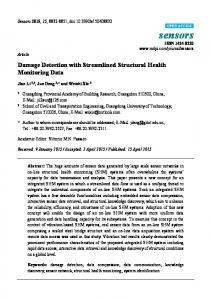
IEEE TRANSACTIONS ON NUCLEAR SCIENCE, VOL. 47, NO. 1, FEBRUARY 2000
X-Ray Detection with a Scintillating YAP-Window Hybrid Photomultiplier Tube C. D’Ambrosio, F. De Notaristefani, H. Leutz, D. Puertolas, and E. Rosso
Abstract—A YAP(YAlO3 : Ce)-scintillating window, coated on its inner surface with an S20-photocathode, seals a cross-focusing hybrid photomultiplier tube (HPMT) equipped with a small p-i-n anode of 2-mm diameter. This new radiation detector separates X-ray lines down to about 2-keV peak energy from the HPMT noise. Its detection efficiency for high gamma energies depends on the YAP-window thickness and amounts to about 18% attenuation at 400-keV energy in the present version. Competitive radiation detectors like silicon photodiodes and silicon drift chambers are discussed and compared to our prototype, with particular attention given to their energy resolution and noise performance, which limits their active area considerably. Index Terms—Hybrid photodetector tubes, scintillating crystals, X- and -ray detection.
I. INTRODUCTION
I
N a recently submitted paper [1], we have demonstrated the advantages of a YAlO3 : Ce window compared to a quartz window at the light entrance faces of two otherwise identical hybrid photomultiplier tubes (HPMT’s). Due to the higher YAP refractive index (1.95) the light transitions from BGOand PbWO4-scintillators have been improved nearly 1.8 times in comparison with those to the other HPMT equipped with a quartz window (1.47 refractive index) of exactly the same dimensions. The present paper reports the results obtained with the same YAP-window HPMT but using it directly as an Xand gamma-ray detector. First investigations of YAP luminescence stimulated via photon excitations have been performed by Weber et al. [2] and the YAP scintillation properties induced by Ce3+-doping have been published by Takeda et al. [3] and more recently by S. Baccaro et al. [4]. The YAP-scintillation spectrum peaks at 360 nm and its light emission is about 40% that of NaI (Tl). YAP monocrystals as X-ray detectors have been studied some years ago by Mares et al. [5], [6]. Excited by X-rays, the scintillation decay time of YAP is with 27 ns [7], about one order of magnitude shorter than with other inorganic radiation detectors. YAP monocrystals are grown by the Czochralski method [7], [8]. The optimum light yields result from the addition of 0.1 to 0.5 wt % CeO2 [7] without changing the decay time. They
Manuscript received August 9, 1999; revised October 28, 1999. This work was supported by INFN, Italy. C. D’Ambrosio, H. Leutz, and E. Rosso are with CERN, EP Division, CH-1211 Geneva 23, Switzerland. F. De Notaristefani and D. Puertolas are with INFN, Sezione di Roma, Rome, Italy. Publisher Item Identifier S 0018-9499(00)01605-1.
are of high hardness (8.6 Mohs), chemically inert, nonhygroscopic, not soluble in acids, and resistant to alkali. These properties qualify YAP plates to be used as windows of vacuum-sealed photocathodes. Based on their scintillation properties, such windows represent efficient low energy X-ray detectors since their light emission reaches without any interface directly the photocathode evaporated onto them. II. DETECTOR LAYOUT The X-ray detector consists of an HPMT1 equipped with a YAP window2 (Fig. 1). The light-detecting S20-photocathode of 19-mm diameter is evaporated on the vacuum side of the YAP window. This window is flat at its outside face and spherically shaped at its photocathode side, according to the cross-focusing geometry, with 3-mm thickness at its center and 5.8 mm at its outer border. Taking an average thickness of 4 mm, the X-ray attenuation amounts to 18% at 400 keV, mainly by Compton scattering. Below 60 keV, a YAP window shows entirely photoabsorption. Focusing electrodes inside the HPMT3 guide the liberated photoelectrons from the photocathode with 13-kV potential difference onto a p-i-n anode of 2-mm diameter and 1-pF capacitance. There, they cross a 0.1-µm-thick insensitive n+-contact layer before being absorbed within the first 2.5 µm of the 300-µm-thick depletion layer. The resulting charge signals are transmitted to a low-noise amplifier outside the HPMT vacuum tube but integrated in its socket to avoid any unnecessary cabling capacitance. The amplifier signals are shaped4 and finally sent to a computer-controlled multichannel analyzer.5 Its ADC is peak-sensing with 8192 channels available. More than ten photoelectrons were directly visualized and could be counted as shown in Fig. 2. This allowed for a precise calibration in terms of photoelectrons versus the channels of the pulse-height analyzer and therefore versus gamma energies. This procedure has been repeated for each X-ray or gamma spectrum by calibrating the analyzer channels via the photoelectron peaks. In this way each total absorption peak could be associated with its corresponding photoelectron number. The excellent signal-to-noise ratio of the HPMT is shown in Fig. 3. The signal of the first photoelectron reaches a peak-to-valley ratio of 15.5 versus the HPMT noise and its FWHM value is 15% although the setup was not shielded 1Assembled by Delft Electronische Produkten (DEP), NL-9300AB Roden, The Netherlands. 2Produced by Crytur Ltd, Turnov, Czech Republic. 3Model PP0275E 4Model 672 EG&G Ortec. 5Model 926 EG&G Ortec.
0018-9499/00$10.00 © 2000 IEEE
D’AMBROSIO et al.: X-RAY DETECTION WITH A SCINTILLATING YAP-WINDOW HYBRID PHOTOMULTIPLIER TUBE
7
Fig. 1. Hybrid photomultiplier tube (HPMT) with its YAP(Ce)-detector window.
against natural gamma background. Such numbers are not achievable with a photomultiplier: Dorenbos et al. show in [9, Fig. 15] a single photoelectron pulse height spectrum measured with an XP2020Q photomultiplier. It results in a 2.6 peak-to-valley ratio and 75% FWHM. D’Ambrosio et al.published a photoelectron spectrum [10, Fig. 4(a)] taken with a Quantacon6 (first dynode: GaAs). The energy resolution of the first photoelectron peak is 28% FWHM with a peak-to-valley ratio of three. In this context, we refrain from reporting on photon yields since they can be estimated only from measured photoelectron yields corrected with the photocathode quantum efficiency and with the uncertain scintillation and photoelectron collections. III. MEASUREMENTS AND RESULTS Radioactive sources were placed at distances between 0.5 and 10 cm in front of the YAP window that was covered by Tyvek (Fig. 1) to provide diffused backscattering of the YAP scintillations toward the photocathode. For each source, a spectrum was recorded and calibrated both in number of photoelectrons and in energy units (keV). The values in photoelectrons of the X- or γ-lines were calculated by fitting the spectra with distributions resulted from the mathematical analysis of the whole detection process [10], [19] (see Figs. 3 and 6 as examples). The dependence of photoelectron numbers from the absorbed energies is displayed in Fig. 4(a). It shows a linear behavior with slope equal to 3.57 [phel/keV] and intercept equal to −0.18 photoelectrons [phel]. Fig. 4(b) shows the blown-up low-energy part of Fig. 4(a). Its linear fit (this time performed between the sulfur 68850,
Burle Electron Tubes, Lancaster, PA.
K-line and the 241Am γ-line) intercepts at −1.78 photoelectrons and at 0.5 keV. The radioactive sources employed are indicated in these figures at their relevant γ- or X-ray energies and at their associated photoelectron numbers. The average characteristic K-radiation of titanium, scandium, calcium, and sulfur were excited by the K-emissions of manganese following the electron capture of 55Fe. Those of terbium, barium, silver, molybdenum, rubidium, and copper were excited by the gamma emission of 241Am. The characteristic K-X-ray peaks are asymmetric (Fig. 5) , and , -emissions. since they are composed of Fig. 5 shows the deconvolution of the measured K-terbium asymmetric peak into two Gaussian distributions representing the K and K emissions. According to the low-intensity contribution of K -emissions, we associate to all K-X-ray ). Energy spectra from some of peaks the K -energies ( the gamma sources are displayed in Fig. 6. IV. DISCUSSION The present YAP-window photocathode configuration (Fig. 1) shows a linear but not exactly proportional energy response of the YAP scintillation process (Fig. 4(b)). Since in the present design the photocathode does not cover the entire scintillating YAP window, with its particular geometry, it is not clear whether this behavior is an intrinsic property of YAP(Ce). Moreover, at low X-ray energies, the ratio of signal-counting rates to background rates decreases, inducing an error on the measured values. For photoelectron yields, our preliminary value of 3.57 photoelectrons/keV exceeds the values of 2.87 photoelectrons/keV (Kirkstead et al. [11]) and 1740 photoelectrons per 662 keV,
8
IEEE TRANSACTIONS ON NUCLEAR SCIENCE, VOL. 47, NO. 1, FEBRUARY 2000
(a)
(b) Fig. 2. (a) Spectral distribution of the average characteristic sulfur K-radiation excited by the manganese characteristic K-emission. The electronic noise affects its shape from around 2 photoelectrons (∼1 keV), since the counting rate is low compared to that indicated for the first six photoelectron peaks of Fig. 3. (b) Average characteristic sulfur K-radiation with manganese excitation rate deduced. The energy scale takes into account the 0.5-keV intercept with the energy axis in Fig. 4(b).
i.e., 2.63 photoelectrons/keV (Dorenbos et al. [9]) but it is lower than the 4.3 photoelectrons/keV (Moszinski et al.) reported by these authors for YAP scintillations, detected with photomultipliers equipped with quartz windows and bialkali photocathodes (R2059 [9], XP2020Q [11], [12]). This is certainly due to still wide variations in light yield of the produced YAP(Ce) windows. The energy resolution and the photoelectron number per energy unit should be improved in future HPMT designs where the photocathode will correctly cover the entire YAP window. Scintillations of inorganic crystals can be also detected with silicon-based photodiodes (PD). The emission spectrum of CsI(Tl) matches the spectral range of light conversion in silicon. Therefore, these crystals are particularly well suited for PD’s
and provide around 70% quantum efficiency in contrast to the 23% achieved with the S20 photocathode [1]. The PD leakage current produces most of the electronic noise and is roughly proportional to the depleted volume. At a fixed depletion depth, this noise increases therefore with the PD cross section which limits the CsI(Tl) diameter to about 10 mm. Bird et al. [13] obtained with 1-cm2 cross-section CsI(Tl) 5.5% FWHM energy resolution at 662 keV. They report a low-energy detection threshold of 35 keV. The Eurorad brochure7 states 60–70-keV threshold for small CsI(Tl) crystals and 6.6% energy resolution for 1-cm2 cross section of PD and CsI(Tl). 7Eurorad,
F-67 037 Strasbourg, France.
D’AMBROSIO et al.: X-RAY DETECTION WITH A SCINTILLATING YAP-WINDOW HYBRID PHOTOMULTIPLIER TUBE
9
Fig. 3. The first seven photoelectron peaks blown up from the inserted characteristic K-radiation of manganese following the 55Fe electron capture. Note the large peak-to-valley ratio and the FWHM energy resolution of the first photoelectron peak. The high counting rate of the first six photoelectron-peaks (330 counts/s) enabled the clear separation from the electronic noise (pedestal).
(a)
(b)
6
Fig. 4. (a) Photoelectron numbers versus the energies of total absorption peaks for several γ- and X-ray emissions. All data are fitted within 3%. (b) Blown-up low-energy part of Fig. 4(a). The data are fitted with: N� photoelectrons 3.57 Energy [keV]—1.78 where 3.57 means the slope in photoelectrons/keV and −1.78 the intercept with the photoelectron axis. The bars indicate 3% variation.
6
=
10
IEEE TRANSACTIONS ON NUCLEAR SCIENCE, VOL. 47, NO. 1, FEBRUARY 2000
Fig. 5. Energy spectrum of Tb. The deconvolution of its measured K-asymmetric peak into two Gaussian distributions representing the K and K emissions is shown. The insert shows the still visible photoelectron peaks, which allow for direct calibration of channel numbers in photoelectron numbers. Escape means the energy peak left from escaping yttrium K-quanta.
Low-energy X-ray detection has been further improved during recent years by the advent of silicon drift chambers (SDC) [14]–[16]. Applied in the X-ray detection mode, they consist of n-type silicon wafers with concentric p+ electrode rings centered by a collecting anode at one side and a continuous p-n junction opposite to it. A reverse bias across the wafer depletes with 300-µm depth the SDC and provides the charge collection field. The outermost electrode ring is supplied with twice the bias voltage and the minimum potential energy falls therefore diagonally from the rear outer edge of the SDC to the center anode at its front side. This distance defines the electron collection time to the anode. Lechner et al. [17] have published results obtained with SDC’s of 3.5-mm cross section (2.1-mm diameter) and 300-µm depletion depth. They achieved 225-eV FWHM for the 5.9-keV manganese K -line at 300K temperature that was completely separated from the K -line. At 223K, this value decreased to 145 eV due to the reduction in thermal electron noise. These resolutions depend on the count rate and increase from 225 eV at 5 × 10 counts/s to 350 eV at 6 × 10 counts/s. The useful X-ray detection energy range falls below 10% attenuation at 28 keV. Increasing the SDC cross section would result in a corresponding rise of energy threshold and resolution. To extend the X-ray detection to higher energies, Fiorini et al. [18] have coupled a 10-mm-high CsI(Tl) scintillator of 3-mm diameter (7-mm cross section) to an SDC of the same diameter. With this detector combination, the authors achieved energy resolutions of 12% FWHM at 60 keV and 7.5% FWHM at 122 keV. The low-energy threshold amounts to 10 keV at room temper-
ature. Increasing the SDC area to 80 mm in order to match it with a CsI(Tl) crystal of 10-mm diameter would increase the thermal SDC leakage current and hence the electronic noise by about one order of magnitude. Achieving in this way reasonable gamma detection efficiency would, therefore, shift the low-energy threshold to higher values and worsen the energy resolution considerably. For the YAP-HPMT employed in this study, the lower limit of the energy resolution is given by the standard deviation , of the Poissonian distribution [19], namely: is the average number of detected photoelecwhere trons, set by the quantum efficiency of the photocathode and the light yield of the YAP window. Moreover, the noise is solely given by the dark counts of the HPMT and affects the first photoelectron peak only. In addition, due to the cross-focusing geometry of the HPMT (Fig. 1), the surface of the silicon diode stays constant independent of the YAP surface at the cathode, thus not increasing the electronic noise of the device. Since the separation between the first photoelectron peak and the others (Fig. 3) is excellent, we can estimate an ultimate lower detection limit (signal-to-noise ratio equal keV gamma energy, if the linear exto 1) to trapolation to zero shown in Fig. 4(b) holds. A last point worth noting is the insensitivity of YAP(Ce) to the humidity of the surrounding air and therefore the possibility of using the input window without a protecting cover. The transmittance through a 100-µm-thick Be protection, covering a NaI(Tl) crystal amounts to only 30% for the sulfur K-radiation. In case of the unprotected YAP(Ce) crystal, all gammas reach its sensitive surface without any attenuation loss.
D’AMBROSIO et al.: X-RAY DETECTION WITH A SCINTILLATING YAP-WINDOW HYBRID PHOTOMULTIPLIER TUBE
11
(a)
(b)
(c) Fig. 6. Three energy spectra taken with the scintillating YAlO3(Ce)-front window of an HPMT (Fig. 1). The 133Ba and 152Eu sources were placed at 0.5-cm distance from the YAlO3(Ce) window. Therefore, the sum peaks of their K-X-rays following their electron capture decays are present. Escape means the energy peak left from K–X absorption near the window surface by an escaping yttrium K–X event.
V. CONCLUSIONS This paper demonstrates that an HPMT sealed with a scintillating YAP window, which is coated on its inner surface with an S20 photocathode, separates X-ray lines down to about 2 keV from the noise. This is first due to the use of a detector window that avoids light losses occurring normally at the interface between it and a separate radiation detector [1]. Second, the cross-focusing HPMT design (Fig. 1) enables to reduce the silicon p-i-n anode to 3.1-mm2 cross section which results in a small leakage current and hence in a low electronic noise level (Fig. 3). The detection efficiency for higher gamma energies depends on the chosen window thickness. The present mismatch between photocathode and
YAP area results in energy resolutions that are not yet representative for this new detector. They will improve in future designs when the areas are adequately matched.
ACKNOWLEDGMENT The authors wish to thank D. Piedigrossi (CERN, EP-TA2) and G. Roubaud (CERN, TIS-RP) for their invaluable help and technical support. The EP-TA2 group at CERN provided the hardware and hosted all the measurements. The authors also acknowledge the fruitful collaboration with their industrial partners.
12
IEEE TRANSACTIONS ON NUCLEAR SCIENCE, VOL. 47, NO. 1, FEBRUARY 2000
REFERENCES [1] C. D’Ambrosio, F. De Notaristefani, H. Leutz, D. Puertolas, and E. Rosso, “Improved light transitions from scintillators to new photocathode-windows,” Nucl. Instrum. Methods. A, vol. 431, p. 455, 1999. [2] M. J. Weber, M. Bass, K. Andringa, R. R. Monchamp, and E. Comperchio, “Czochralski growth and properties of YAlO3 laser crystals,” Appl. Phys. Lett., vol. 15,, p. 342, 1969. [3] T. Takeda, T. Miyata, F. Muramatsu, and T. Tomiki, “Fast decay UV phosphor-YAlO3 : Ce,” J. Electrochem. Soc., vol. 127, p. 438, 1980. [4] S. Baccaro, A. Cecilia, M. Montecchi, T. Malatesta, F. de Notaristefani, S. Torrioli, and F. Vittori, “Refractive index and absorption length of YAP : Ce scintillation crystal and reflectance of the coating used in YAP : Ce single-crystal matrix,” Nucl. Instrum. Methods A, vol. 361, p. 209, 1995. [5] J. A. Mares, M. Nikl, and K. Blazek, “Green emission band in Ce3+doped yttrium aluminum perovskite,” Phys. State Sol. (a), vol. 127, p. K65, 1991. [6] J. A. Mares, J. Chval, M. Nikl, and G. Boulon, “Identification of trace impurities in pure and doped YAlO3 and YAl5O12 crystals by their fluorescence and by the EMA method,” Czech. J. Phys., vol. 43, p. 683, 1993. [7] V. G. Baryshevsky, M. V. Korzhik, V. I. Pavlenko, A. A. Fyodorov, S. A. Smirnova, O. A. Egorvcheva, and V. A. Kachanov, “YAlO3 : Ce-fastacting scintillators for detection of ionizing radiation,” Nucl. Instrum. Methods B, vol. 58, p. 291, 1991. [8] J. Kvapil, J. Kvapil, J. Kubelka, and R. Autrata, “The role of iron ions in YAG and YAP,” Cryst. Res. Technol., vol. 18, p. 127, 1983. [9] P. Dorenbos, J. T. M. de Haas, and C. W. E. van Eijk, “Nonproportionality in the scintillation response and the energy resolution obtainable with scintillation crystals,” IEEE Trans. Nucl. Sci., vol. 42, p. 2190, 1995.
[10] C. D’Ambrosio, T. Gys, H. Leutz, D. Puertolas, and S. Tailhardat, “Photoelectron counting with small diameter scintillating fibers,” Nucl. Instrum. Methods A, vol. 332, p. 134, 1993. [11] J. A. Kierstead, S. P. Stoll, and C. L. Woody, “Light output and radiation damage in a YAlO3 : Ce crystal,” in Scintillator and Phosphor. Materials Symp., vol. 348, San Francisco, CA, USA, Apr. 6–8, 1994, p. 469. [12] M. Moszynski, M. Kapusta, D. Wolski, W. Klamra, and B. Cederwall, “Properties of the YAP : Ce scintillator,” Nucl. Instrum. Methods A, vol. 404, p. 157, 1998. [13] A. J. Bird, T. Carter, A. J. Dean, D. Ramsden, and B. M. Swinyard, “The optimization of small CsI(Tl) gamma-ray detectors,” IEEE Trans. Nucl. Sci., vol. 40, p. 395, 1993. [14] J. Kemmer, P. Burger, R. Henk, and E. Heijne, “Performance and application of passivated ion-implanted silicon detectors,” IEEE Trans. Nucl. Sci., vol. NS-29, p. 733, 1982. [15] E. Gatti and P. Rehak, “Semiconductor drift chamber—An application of a novel charge transport scheme,” Nucl. Instum. Methods, vol. 225, p. 608, 1984. [16] P. Rehak, E. Gatti, A. Longoni, J. Kemmer, P. Holl, R. Klanner, G. Lutz, and A. Wylie, “Semiconductor drift chambers for position and energy measurements,” Nucl. Instrum. Methods A, vol. 235, p. 224, 1985. [17] P. Lechner, S. Eckbauer, R. Hartmann, S. Krisch, D. Hauff, R. Richter, H. Soltau, L. Struder, C. Fiorini, E. Gatti, A. Longoni, and M. Sampietro, “Silicon drift detectors for high resolution room temperature X-ray spectroscopy,” Nucl. Instrum. Methods A, vol. 377, p. 346, 1996. [18] C. Fiorini, A. Longoni, F. Perotti, C. Labanti, P. Lechner, and L. Struder, “Gamma ray spectroscopy with CsI(Tl) scintillator coupled to silicon drift chamber,” IEEE Trans. Nucl. Sci., vol. 44, p. 2553, 1997. [19] C. D’Ambrosio, C. Ercoli, S. Jaaskelainen, G. Lecoeur, H. Leutz, R. Loos, D. Piedigrossi, D. Puertolas, E. Rosso, and R. Schomaker, “A HPMT based set-up to characterize scintillating crystals,” Nucl. Instum. Methods A, vol. 434, p. 387, 1999.