drift bounded to ±1.1dB and low power consumption. II. SYSTEM ARCHITECTURE. The architecture of a log-amp detector is based on a cascade of N gain cells ...
A 39 dB DR CMOS Log-Amp RF Power Detector with ±1.1 dB Temperature Drift from -40 to 85◦C Eric Muijs∗† , Paulo Silva† , Arie van Staveren† , and Wouter Serdijn∗ ∗ Delft
University of Technology, Delft, the Netherlands Instruments, Delft, the Netherlands
† Texas
Antenna
Abstract—This paper presents a temperature compensated logarithmic amplifier (log-amp) RF power detector implemented in CMOS 0.18 µm technology. The input power can range from -50 to +10 dBm for RF signals ranging from 100 MHz to 1.5 GHz. This design attains a typical DR of 39 dB for a ±1 dB logconformance error (LCE). Up to 900 MHz the temperature drift is never larger than ±1.1 dB for all 24 measured samples over a temperature range from -40 to +85◦ C. The current consumption is 6.3 mA from a 1.8 V power supply and the chip area is 0.76 mm2 .
To accurately set the output power of a PA in handsets, a power control loop is often used. A coupler senses a fraction of the output RF signal and feeds it to an RF power detector (Fig. 1). It’s output is a measure of the average peak value of the input RF signal. Knowledge about the modulation type employed allows for the accurate calculation of the transmitted power. Log-amp detectors in Bipolar technology present good temperature stability for RF applications [1], [2]. CMOS logamps for RF power-detection so far published fail to demonstrate consistent performance over a wide temperature range [3], [4]. This prototype IC demonstrates that a temperature compensated log-amp RF power detector can be designed using standard CMOS technology while attaining a temperature drift bounded to ±1.1 dB and low power consumption.
VGA RF
PA 50 Ω
Gain Control Digital Control
ADC
~30 dB attenuation
RF detector
Transmitted power
I. I NTRODUCTION
Coupler
Fig. 1: Transmitted-power control loop
Increasing the input signal to EkD /A3 will clip the output of the last two detector cells to IbiasD . Consequently, for every multiplication of the input signal magnitude by A, a linear increase of the output current equal to IbiasD is expected. A piece-wise linear approximation of a logarithmic function is obtained. This logarithmic transfer can be represented by a linear relation between Vout and the input power Pin expressed in dBm: Vout [V] = Kslope (Pin − P0 ) , (3) where Kslope and P0 are given by: Kslope [V/dB]
=
P0 [dBm]
=
IbiasD Rout , (4) 20 log(A) � � EkD 20 log √ + 30 . (5) 50 Ω · AN +1
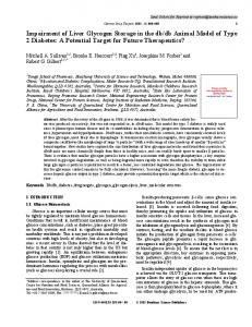
II. S YSTEM ARCHITECTURE The architecture of a log-amp detector is based on a cascade of N gain cells (A), N+1 detector cells (D), an output low-pass filter (LPF1) to reject high-frequency components at the output and finally an offset cancellation loop around the cascade of gain cells and another low-pass filter (LPF2). In this design N = 4, as shown in Fig. 2. The transfer characteristic of A and D are respectively: ( A · Vin-A , if |Vin-A | < EkA , Vout-A [V] = (1) A · EkA , if |Vin-A | ≥ EkA , ( β · V 2 , if |Vin-D | < EkD , (2) Iout-D [A] = 4 in-D IbiasD , if |Vin-D | ≥ EkD ,
A. Temperature compensation To implement a log-amp detector for which the transfer characteristic is temperature independent, both the slope (Kslope ) and the intercept power (P0 ) should be kept constant over temperature. This is achieved by temperature stabilization of both the gain cells and the detector cells and by temperature scaling of the input/output signals of the log-amp detector core (Fig. 2). Fig. 3 shows the architecture of the complete temperature compensated log-amp detector.
Vin
in which A is the voltage gain of the gain cell, Ek is the input referred clipping voltage (knee voltage) and in CMOS technology β = µCox W/L. In this design AEkA > EkD is chosen. For an input signal with amplitude EkD /A4 , only the last detector cell reaches its maximum output current, IbiasD .
978-1-4799-0645-1/13/$31.00 ©2013 IEEE
287
Idet Vdet Rout Fig. 2: Log-Amp Detector Core
Vdd
Iout Vout
Vin
R1
Idet
R2 M6
Rout
bias-cascode
Vout+ M5
Vout-
Fig. 3: Log-Amp Detector with temperature compensation M3
1) Gain Cell: The gain (A) variation over temperature affects the transfer’s slope (4) and intercept (5). To keep both parameters constant over temperature, the gain cell (Fig. 4) should be designed to attain a voltage gain gm · R that is constant over temperature:
M4
Vin+
VinM1
M2
bias-GC M7
R3
A(T )
= gm (T ) · R(T ) r W µ(T )Cox IbiasA (T ) · R(T ) , = L
Substitution of (9) into (5) results in: � � EkD (T ) P0 (T ) = 20 log √ + 30 50 Ω · S(T ) · A5 √ � � 2 K0 = 20 log √ + 30 , 50 Ω · S0 · A5
R4
R5
Fig. 4: Circuit of Gain-cell (A)
(7)
The temperature dependence of EkD on both β(T ) and R(T ) needs to be compensated for in (5). This can be achieved through the front-end PTIM voltage scaler. The transfer of the input voltage scaler is given by: S0 . β(T )R(T )
IbiasA
(6)
where µ(T ) = µ0 (T /Tref )Nµ models the temperature dependence of the mobility with 1.5 < Nµ < 2 [5] and R(T ) represents the temperature behavior of all resistors in this design (except the resistors in the front-end scaler). If current IbiasA (T ) is designed to have a temperature dependence proportional to the inverse mobility (PTIM) and R(T )−2 , the gain A becomes to a first order constant over temperature. 2) Input PTIM Voltage Scaler: After temperature compensation, the maximum output swing of every gain cell presents a PTIM temperature dependence. Consequently the gain and detector cells, except the front-end cells, experience a maximum input voltage with PTIM temperature behavior. Therefore a PTIM voltage scaler in front of the log-amp detector core is required. 3) Detector Cell: Detector bias current IbiasD and knee voltage EkD appear in the expressions for slope (4)pand intercept (5) respectively. Rewriting (2) yields EkD = 4IbiasD /β . Because the maximum output voltage of the gain cells exhibit a PTIM behavior, EkD should follow the same temperature behavior. This can be achieved using a PTIM bias current IbiasD = K0 L/(Cox W R2 (T )µ(T )). The knee voltage becomes: s √ 4IbiasD (T ) 2 K0 EkD (T ) = = . (8) β(T )R(T ) Cox W L µ(T )
S(T ) =
M9
M8
IbiasA
IbiasA
4) PTM Current scaler: The output current Idet of the logamp detector core presents the same PTIM dependence as IbiasD . In order to obtain a log-amp detector with a constant transfer over temperature, a proportional to mobility (PTM) current scaler is required between the log-amp detector core and the final I-V conversion (Fig. 3): Iout-CONST = Idet-PTIM · (ICONST /IPTIM ) .
(12)
III. C IRCUIT D ESIGN A. Input PTIM Voltage Scaler A resistor π-network, with a 50 Ω input impedance and 5.7 dB attenuation, implements the passive front-end voltage scaler by employing positive- and negative-temperature coefficient resistors. The first-order temperature behavior of the desired relation (9) can be approximated by controlling the resistor values RPTC and RNTC : S(T ) =
RPTC RNTC · (TCP − TCN ) . (RPTC + RNTC )2
(13)
B. Gain Cell The circuit of the gain cell, shown in Fig. 4, is a differential pair with cascodes, the latter to improve the bandwidth by decreasing the Miller multiplication of CGD of M1/M2 seen at the input of the gain cell. The voltage followers provide a lower common-mode output voltage needed to bias the next gain cell. To limit the VGS voltage drop, the voltage followers were implemented with isolated NMOS devices (VBS = 0). C. Detector Cell
(9)
(10) (11)
which yields a temperature independent intercept power P0 .
The circuit of the detector cell is depicted in Fig. 5. It is an NMOS version of the detector circuit from [6]. Differently from it’s bipolar counterpart, where EkD = 4VT , EkD is a function of transistor size and bias current in a MOS implementation. For a sinusoidal input signal Vin = VP sin(ωp t), were VP ≤ EkD , the detector output current can be expressed by: � β βVP � 1 − cos(2ωp t) [A] , (14) Iout = VP sin2 (x) = 4 8
288
Vdd
Vdd
Iout+
IoutR7
R14
Idet
R15
ICONST
IPTIM
(PTIM)
OA4
Vin+ M10
M11
M12
M15
M16
M17
M18
M13 OA1
R6
OA3
M23
1V
Iout
(CONST)
OA1
M25
M24
R7
Vin-
Q1
M21
M22
IbiasA
Q2
Q3
Q4
OA6
bias-GC
Vout R9
bias-DET
OA2
M14
RX
R10
IbiasD
M19
R8
R12
R13 Cfilt
gnd OA5
Fig. 5: Circuit of detector-cell (D) Fig. 6: Circuit of PTIM current generator.
200 mV
Fig. 8: Circuit of PTM current scaler and I-V converter.
which contains a DC and a double frequency component (2ωp ). After low-pass filtering only the DC component remains. The current output of the detector (βVP /8) is thus a measure of the peak amplitude of the input signal. D. PTIM Bias Generator From (5) it follows that the intercept is inversely proportional to A5 . Small variations of the gain will yield relatively large intercept shifts over temperature, which requires an accurate constant-gm bias circuit. The chosen architecture for constant-gm biasing is shown in Fig. 6. The current through transistors M21 and M22 is given by [7]: √ 1 2LM21 ( n − 1)2 IPTIM (T ) = 2 , (15) R (T ) µ(T )Cox WM21 n where n is the ratio between the areas of M21 and M22. To increase the accuracy of the bias current two phenomena should be accounted for in the PTIM bias generator: mobility degradation and velocity saturation, which are both short channel effects. The effective mobility is given by [5]: µ0-eff =
µ0 vmax L , vmax L(1 + θVOV ) + µ0 VDS
Rfilt
M20
mobility is thus dependent on the MOSFET’s biasing conditions. The overdrive voltage of the gain cell transistors M1/M2 is equal to the overdrive voltage of M21/M22 in the bias generator if they have the same current density and the same unit device. Simulation results in Fig. 7a show the gain error over temperature for different L sizes inside the bias generator (same W/L ratio). When M21/M22 use the same unit device as M1/M2, the gain error over temperature reduces to