Flip Flop. Controller. (FFC). sPI. I2C. Volatile Logic. Non volatile Logic. Flip flop Controller. JTAG. 8KB. sRAM. MODE sleep. /Wake up. JTAG. sPI signal. PIO&PC.
A 3us Wake-up Time Nonvolatile Processor Based on Ferroelectric Flip-Flops Yiqun Wang ∗ Yongpan Liu∗ Shuangchen Li∗ Daming Zhang∗ Bo Zhao ∗ Mei-Fang Chiang† Yanxin Yan† Baiko Sai† Huazhong Yang∗ {ypliu,yanghz}@tsinghua.edu.cn {baiko.sai,meifang.chiang}@dsn.rohm.co.jp ∗ Tsinghua National Laboratory for Information † LSI Development Headquarters, Rohm Co., Ltd. Science and Technology, EE Dept.,Tsinghua University Yokohama, 222-8575, Japan Beijing, 100084, China Abstract—Nonvolatile processors offer a number of desirable properties including instant on/off, zero standby power and resilience to power failures. This paper presents a fabricated nonvolatile processor based on ferroelectric flip-flops. These flipflops are used in a distributed fashion and are able to maintain system states without any power supply indefinitely. An efficient controller is employed to achieve parallel reads and writes to the flip-flops. A reconfigurable voltage detection system is designed for automatic system backup during power failures. Measurement results show that this nonvolatile processor can operate continuously even under power failures occurring at 20 KHz. It can backup system states within 7 μs and restore them within 3 μs. Such capabilities will provide a new level of support to chip-level fine-grained power management and energy harvesting applications.
I. I NTRODUCTION In embedded or mobile applications, low power processors can be shut down to eliminate leakage power. However, the states in volatile registers and local memories will be lost or have to be backed up into centralized nonvolatile memories (NVM) [1], [2]. The backup process introduces nontrivial power and performance overheads when writing or reading register states into or from NVM during the sleep or wake-up stage. To reduce power and performance overheads experienced by centralized NVM architectures, the concept of distributed nonvolatile processor (NVP) is proposed [3]–[6]. An NVP introduces a set of distributed nonvolatile flip-flops (NVFF) used to backup regular register contents. By storing the system state in local NVFFs, the state can be stored and recalled in parallel within several cycles. In theory, an NVP can backup the data in every NVFF in parallel so it has the potential to reduce the sleep and wake-up time to several nanoseconds, which provides the capability of ”instant” sleep and wakeup. Furthermore, the local data transferring can reduce power consumption between power on and off which provides NVP with high resilience to power failure and high flexibility for power management. Therefore, NVP can help to support more efficient fine-grained power management and energy harvesting systems. Recently, Rohm first implemented a nonvolatile counter based on ferroelectric flip-flops [3]. Wang et.al. [4] introduced a nonvolatile processor (NVP) with ferroelectric flip-flops using a compare-and-write policy. Afterwards, Yu et.al. [5] proposed a floating gate based NVP. Furthermore, reference [6] This work was supported in part by the NSFC under grant 60976032, National Science and Technology Major Project under contract 2010ZX03006003-01, International Cooperation from ROHM Inc. and High-Tech Research and Development (863) Program under contract 2009AA01Z130.
978-1-4673-2213-3/12/$31.00 ©2012 IEEE
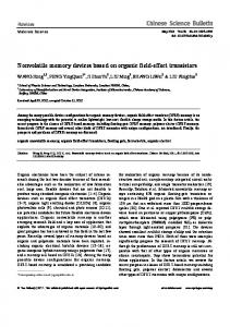
presented a compare-and-compress architecture to reduce the NVP’s area. To our best knowledge, none of a silicon proved NVP had been reported before. Specifically, we make the following contributions in this paper: 1) We present the first fabricated nonvolatile processor with zero standby power, 7μs sleep time and 3μs wake-up time. The low switching overhead of the NVP attributes to careful design of the FF controller and the voltage decision system. 2) We demonstrates that the NVP can achieve over 30100x speedup on the wake-up/sleep time and over 70x energy savings on the data backup and recall operations when compared with an existing industry processor. Meanwhile the NVP exhibits comparative performance and power consumption in normal operations. The rest of this paper is organized as follows. Section II discusses the overall architecture of the nonvolatile processor and the voltage detection unit. We then describe the circuits of ferroelectric flip-flops (FeFF) and the nonvolatile controller in Section III. The chip evaluation results are presented in Section IV. We conclude the paper in Section V. II. A RCHITECTURE This section presents the overall NVP architecture and illustrates a configurable voltage detection system, which signals the NVP to backup the system state automatically under power failures. A. Overall NVP Architecture Fig. 1 shows the block diagram of the entire NVP. It contains a MCS51 instruction set compatible core, which consists of an MCU controller, an 8-bit arithmetic logic unit (ALU), several timers and counters, a serial interface, a 128Byte register file and an 8K-Byte static random access memory (SRAM). There are two peripherals, SPI and I2C modules, connected to the core via a Wishbone bus. A ”JTAG” module is added to support online debug via scan chains. The ”Mode” module is used to control the operating mode of the processors, including the volatile mode, the nonvolatile mode and the debug mode. In this chip, we replace all flip-flops in the core and the 128Byte register file with nonvolatile ferroelectric devices. They are denoted as the nonvolatile logic domain in Figure 1. The SRAM is used as a secondary data memory and it doesn’t store the system state, so we don’t replace it to save area. However, it can be replaced with ferroelectric RAM (FeRAM) in future work. Similarly we don’t need to keep the states of
149
63,� 6LJQDO
�.% 65$0
,�&� 6LJQDO
63,
,�&
&ON
-7$*
3/
&ON 'RXW
'LQ
-7$*
0�
&ON
�
)H&DS
D E
&ON 'RXW
�
0�
3/
:LVKERQH�%XV
6WDQGDUG�7ZR�6WDJH�)OLS�IORS
3,2 3& 7;'� 5;' 7��7�
0&8B&21752//(5 �,'� �)60� �5HJ)LOH�&RQWURO 6HULDO ,QWHUIDFH 7LPHU� &RXQWHU
9RODWLOH�/RJLF
$/8
���% 5HJLVWHU� )LOH
1RUPDO
6OHHS )OLS�)ORS� �:DNH�XS &RQWUROOHU �))&
6WRUH
3RZHU�GRZQ
1RUPDO
5HFDOO
9'' &/. '
6WRUH�LQWR�)H&DS
3/
)OLS�IORS�&RQWUROOHU
5HFDOO�IURP�)H&DS
3&+
Fig. 1.
1RQYRODWLOH�6WRUDJH
�D �3URSRVHG�IHUURHOHFWULF�IOLS�IORS�VWUXFWXUH
5:
1RQ�YRODWLOH�/RJLF
3&+
02'(
Overall architecture of nonvolatile processor 4
remote peripherals SPI and I2C, so they are in the volatile logic domain. The flip-flop controller (FFC) is used to generate controlling signals to both FeFFs and volatile flip-flops (VFFs) after receiving the sleep or wake-up signals. We will describe its mechanism in Section III. B. Configurable Voltage Detection System In this subsection we will discuss how to generate the sleep or wake-up signal for the NVP to backup its system state when power failures happen. An configurable voltage detection system (CVDS) is proposed to generate those two signals. The CVDS architecture is shown in Fig. 2(a), which contains two configurable units. The first one is a switched capacitor array attached to the power line. The configurable capacitor, denoted as CP L , provides the data backup energy to NVP by keeping the voltage above the operating threshold after the power is cut down. The other one, denoted as CV D , is another switched capacitor array used in the voltage detection circuit. The voltage detection circuit could detect the power failure and regain. It would generate the ”Sleep/Wake-up” signal (0 denotes sleep, 1 denotes wake-up) at a certain time (Tplh ) after the ”VDD” passes the operating threshold. The value of Tplh is determined considering the tradeoff between system reliability and backup speed. The control words for those switched capacitor arrays are given by external input switches, which is maintained by users. Fig. 2(b) shows the waveform during the sleep and wake-up actions and the timing diagram influenced by CP L and CV D . Measurement results on the CVDS architecture are given in section IV-B. III. C IRCUIT D ESCRIPTION We will describe two major circuit structures of NVP different from conventional processor: the ferroelectric flipflop and the flip-flop controller. A. Ferroelectric Flip-flop Flip-flops could impact the NVP’s performance, power and reliability, therefore they should designed carefully. The FeFF used in this chip is shown in Fig. 3(a) [6]. It adopts a hybrid CMOS and ferroelectric technology, consisting of a standard master-slave D flip-flop (DFF) and a backup ferroelectric capacitors (FeCap). The detailed working mechanism of this
�E 7LPLQJ�FKDU�RI�VWRUH�DQG�UHFDOO
Fig. 3.
Modeling of ferroelectric flip-flop
FeFF is described in the work [4] In this circuit, the differential architecture help to improve the reliability and performance. The circuits are simulated by HSPICE, and the waveform of this circuit during a store and restore operation is shown Fig. 3(b). B. Flip-flop Controller The flip-flop controller (FFC) is used to generate sequential controlling signals to FeFF in sleep and wake-up actions. Fig. 4(a) shows the block diagram of FFC. It is composed of a timing block and a signal generating finite state-machine (FSM). The timing block is self-timed by the inverter chain and the three timers provide overflow signals (Tov1-Tov3) to the FSM. The FSM generates the controlling signals (”RW”,”PL”,”PCH”) based on Tov1-Tov3 to meet the sequential requirements shown in Fig. 4(c). The input ”Sleep/Wake-up” tells the FSM whether it should be execute sleep sequence or wake-up sequence. The output ”CG” is the clock-gating signal to both FeFFs and DFFs. Fig. 4(b) shows the interconnection between FFC and the flip-flops. The ”CG” signal gates the clock of both FeFF and volatile FF during the store and recall actions as is shown in Fig. 4(c). It can maintain the data of FeFF during store action to prevent writing uncertainty and hold system stably during recall action to guarantee precise recovery. IV. M EASUREMENTS A. Test Setup and Performance Overview The nonvolatile processor, named as THU1010N, has been fabricated using the ROHM’s 0.13μm CMOS-ferroelectric hybrid process. Fig. 5(a) shows its photomicrograph. We evaluate the processor with a suite of embedded benchmarks for sensor networks, such as FFT, FIR and Zigbee MAC protocol. We measured the maximum operating frequency, the average power consumption and the sleep/wake-up metrics with controlled power supplies. We illustrate the general
150
3RZHU�RQ�WLPH 3RZHU
9''
7ULVH
9''
7IDOO
ĂĂ
3,2
&3/
)URP� ([WHUQDO 6ZLWFKHV
9ROWDJH�'HWHFWLRQ &LUFXLW
6OHHS� :DNH�XS
9UHI
193
9''
7UHFDOO
6OHHS� :DNH�XS
7SKO
7SOK
7VWRUH
6OHHS� :DNH�XS
� �
9UHI
ĂĂ
7ULVH�7IDOO� �9ROWDJH�7UDQVLWLRQ�WLPH�RQ�SRZHU�OLQH�GHFLGHG�E\�&3 3/ 7SOK�7SKO� �9ROWDJH�'HWHFWLRQ�VSHHG�GHFLGHG�E\�&9 9' 7VWRUH�7UHFDOO� �'DWD�VWRUH�DQG�UHFDOO�WLPH
&9' �D �$UFKLWHFWXUH�RI�FRQILJXUDEOH� YROWDJH�GHWHFWLRQ�V\VWHP
Fig. 2.
,QWHUQDO�FORFN
7LPLQJ�EORFN
7LPHU�
7RY�
7LPHU�
7RY�
7LPHU�
7RY�
�E �7LPLQJ�FKDUW�RI�V\VWHP�OHYHO�VOHHS�ZDNH�XS�SURFHVV�
Architecture and controlling timing chart of configurable voltage detection system
nonvolatile architecture of NVP will provide much better performance than the existing centralized nonvolatile storage. It is quite promising for energy harvesting and power management applications.
5:
6LJQDO� JHQHUDWLQJ� )60
3/ 3&+ &*
6OHHS�:DNH�XS �D �%ORFN�GLDJUDP�RI�))& �6WRUH��6OHHS )H))
5: 3/ 3&+
19� &RQWUROOLQJ� 6LJQDOV
)OLS�IORS &RQWUROOHU &* �))&
5: 3/ 3&+ &ON
RW PL
9RODWLOH�))
&ORFN
*DWHG FORFN
&ON
THU1010N
TI-MSP430-5series with Flash
TI-MSP430 with FRAM
I/O Pin Number Capacity of Memory
100 1607-bit FeFF 8KB SRAM
64 − 80 2-16KB SRAM 32-128KB FLASH
24 − 40 16KB FRAM
Non-volatilizaion level
Register level
Memory level
1KB SRAM Memory level
25MHz 1.8V-3.6V 450μW @1MHz 0.18μA
24MHz 2-3.6V 200μW @1MHz 0.32μA
6ms 3ms
212μs 310μs
ಹಹ
Clock
General Statistics
Gated_clock
�E �,QWHUFRQQHFWLRQ�EHWZHHQ�))&�DQG�))V
Fig. 4.
Microprocessor Type
PCH
4
'
TABLE I OVERALL P ROPERTIES OF N ONVOLATILE P ROCESSOR C HIP AND C OMPARISON R ESULTS
CG
4
'
6OHHS� :DNH�XS
5HFDOO��:DNH�XS�
Sleep(0)/ Wake-up(1)
�F �7LPLQJ�FKDUW�LQ�VWRUH�DQG�UHFDOO�DFWLRQV
Block diagram of flip-flop controller
Basic Properties
parameters of THU1010N, as well as some comparison results in Table I.
Sleep/Wake-up Time
Maximum Clock Frequency 25MHz VDD for Core 0.9V-1.5V Active Power 160μW @ 1MHz Standby Power 0 Sleep time Wake-up time
7μs 3μs
��XV
$/8
7LPHU )&&
0DLQ &RQWUROOHU
63,�,�& 8$57
19 5HJLVWHU )LOHV
�.% 65$0
D �7+8����1�PLFURJUDSK
Fig. 5.
B. Measurements of Sleep and Wake-up Time
9''
6OHHS� :DNH�XS
'DWD 6WRUH
'DWD 5HFDOO
&RXQWLQJ 2XWSXW
E �&RQWLQXRXVO\�FRXQWLQJ�XQGHU� ��.+]�LQWHUUXSWHG�SRZHU�VXSSO\
Micrograph and general design statistics of THU1010N
Table I compares the NVP chip with a popular industrial processor ”MSP430” [1] and an emerging processor based on FeRAM ”MSP430FR series” [2]. The sleep and wakeup time of ”MSP430” come from the switch time between LPM4.5 mode and active mode (more details in [1], [2]). The result shows that the NVP chip achieves comparative operating parameters during the normal mode. However, it has tremendous advantages in sleep/wake-up time, which shows 100-1000x speedup in the sleep time and 30-100x speedup in the wake-up time. In the chip level, we only need a few microsecond to switch from the power down mode to the active mode. Therefore, we can conclude that the distributed
This section will evaluate the sleep and wake-up time of the processor in details. The first part is to show the chiplevel performance, which is critical for the chip-level power gating issue. The other part is to demonstrate the system-level performance, which is related to the voltage detection system. To measure the chip-level sleep and wake-up time, we use a pattern generator to provide both ”VDD” and ”Sleep/Wakeup” signals. In the experiments, the NVP executes a counting program under a square wave power supply. By shorten the pulse width of ”VDD” and the time interval between ”VDD” and ”Sleep/Wake-up”, we can measure the minimal chip-level sleep and wake-up time. The result shows that the sleep and wake-up time is 7μs and 3μs under 1.5V power supply. Moreover, we discover that the core voltage may impact the sleep and wake-up speed. Fig. 6 shows the sleep and wakeup time under different voltage supplies. As we can see, the lower voltage would lead to a slower speed. It is because the delays of both FeFF and FFC circuit become larger. However, the sleep and wake-up time can still be smaller than 20μs and 10μs under a 0.8V supply voltage. Therefore, the physical limitation comes from the devices, such as the FeFFs and FFC circuit. Compared with the several milliseconds backup time in the centralized structure, the microseconds
151
−3
18
1.4
Wake−up time
Fault Region
1.2
Sleep time
Minimal Power−on time (s)
Sleep/Wakeup Time (us)
16
x 10
14 12 10 8 6
1
PASS
0.8
0.6 C =10pF VD
0.4
FAIL
CVD=22pF C =50pF VD
0.2
4 2 0.8
Fig. 6.
1
1.2 1.4 1.6 Core Supply Voltage (V)
1.8
0 0.047 0 0.1
2
NVP sleep and wake-up time under different voltage supply
0.2
0.3
0.4
0.5
0.6
0.7
0.8
Power Line Capacitor −− CPL(F)
0.9
1 x 10⁻⁵
Fig. 7. The minimal power-on time for system accuracy under different capacitance values
switching overheads will provides much more power savings opportunities for the fine-grained on-chip power management. To demonstrate the system-level sleep and wake-up time, we consider the overheads from the power supply as well as the voltage detection. In this experiment, we provide a square wave power supply to the board, and the ”Sleep/Wakeup” signal should be automatically generated by the voltage detection circuit. Figure 5(b) shows that it can continuously count under the square wave ”VDD” of 20Khz. It implies that the NVP can recover the whole system state, continue to compute then backup the system state within only 25μs. Below, we will evaluate the impacts of capacitors CP L and CV D under different power conditions. Fig 7 shows the minimum power-on time under different CP L and CV D . The power-on time should be larger than the sum of power stabilization time, voltage detection time and chip intrinsic sleep and wake-up time. The CP L impacts the ”VDD” power stabilization via the RC-constant, so the minimal requested power-on time decreases when CP L gets lower. However, if the CP L is smaller than 470nF , it cannot provide sufficient energy for data backup that the system goes to the false region. The CV D impacts the voltage detection time via its RC-constant, so the requested power-on time decreases when CV D gets lower. The CV D cannot be smaller than 10pF for the power and clock stabilizing concern. As we can see, the minimal requested power-on time (> 100μs) is much larger than the chip intrinsic sleep and wake-up time (< 10μs) because the most dominating factor in the system-level is the power and clock stability speed, instead of the inner chip circuit speed.
TABLE II DATA STORE AND RELOAD ENERGY CONSUMPTION OF THREE DIFFERENT DATA BACKUP LOCATIONS . Data Bakcup Location Data store energy(nJ) Data recall energy(nJ)
FeFF (NV-registers) 23.1nJ 8.1nJ
Off-chip Flash 2060μJ 1.3μJ
On-chip Flash 445μJ 0.6μJ
with frequent power downs, such as wireless sensor network (WSN). Assuming the node will be powered down one time per minute, it will consume 1.12kJ energy for a Flash memory based node during one year lifetime. However, only 17J energy is consumed in the NVP solution. V. C ONCLUSIONS Nonvolatile processor implements nonvolatile technology in the register level which brings huge improvements to the backup speed and the energy efficiency. We fabricated a ferroelectric nonvolatile processor and the measured results show that it achieves a 3μs sleep and 7μs wake-up time in the chip level, as well as several nanowatts energy consumption during those backup operations. Those metrics surpass all the existing solutions by 100-10000 times. Those features are quite promising for fine-grained power management and energy harvesting applications. In future, more works will be done to reduce the sleep/wake-up time to several nanoseconds, which is the physical limitation of the device. Moreover, the voltage detection circuit can be optimized to shorten the response time for unexpected power intervals.
C. Measurements of Sleep and Wake-up Energy
VI. ACKNOWLEDGEMENT Thanks for many helpful suggestions from Prof. Xiaobo Sharon Hu.
The energy consumption for each sleep and wake-up operation is also a key property for the power management. We compare the NVP with two popular data backup methods: 1) off-chip Flash memory; 2)on-chip Flash memory. Table II shows the energy consumption to store and recall 1607 bits data (the FeFF number in the NVP processor) with those three methods. Comparing with other two methods, the proposed distributed architecture can decrease the energy consumption by 19000 times in the data store and 74 times in the data recall. These results conclude that much higher energy efficiency can be obtained if we using nonvolatile registers instead of the centralized nonvolatile memory. The tremendous advantages in the energy consumption show that the NVP is an excellent candidate for applications
[1] TI, “datasheet of msp430f522x mixed signal microcontrollers,” 2009. [2] ——, “datasheet of msp430fr573x mixed signal microcontrollers,” 2011. [3] Rohm Co., Ltd., “Rohm Demonstrates Nonvolatile CPU,” Website: http://techon.nikkeibp.co.jp/english/NEWS EN/20071004/140206/. [4] J. Wang, Y. Liu, H. Yang, and H. Wang, “A compare-and-write ferroelectric nonvolatile flip-flop for energy-harvesting applications,” in Green Circuits and Systems (ICGCS), 2010 International Conference on. IEEE, pp. 646–650. [5] W. Yu, S. Rajwade, S. Wang, B. Lian, G. Suh, and E. Kan, “a non-volatile microcontroller with integrated floating-gate transistors,” in Proceedings of the 5th Workshop on Dependable and Secure Nanocomputing. ACM Press, 2011, pp. 1–4. [6] Y. Wang, Y. Liu, Y. Liu, D. Zhang, S. Li, B. Sai, M.-F. Chiang, and H. Yang, “A compression-based area-efficient recovery architecture for nonvolatile processors,” in Design, Automation Test in Europe Conference Exhibition (DATE), 2012, march 2012, pp. 1519 –1524.
R EFERENCES
152