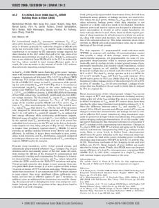
E-B junction. This creates diffusion currents, holes flow from. Base to Emitter and electrons flow from Emitter to Collector. The electron current is higher than the ...
IEEE ELECTRON DEVICE LETTERS, VOL. 16, NO. 5, MAY 1995
169
A Bipolar Load CMOS SRAM Cell for Embedded Applications A. S. Shubat, Member, IEEE, R. Kazerounian, Member, IEEE, R. Irani, Member, IEEE, A. Roy, Member, IEEE, G. A. Rezvani, Member, IEEE, B. Eitan, Member, IEEE, and C. Y. Yang, Senior Member, IEEE
Abstract-This paper presents a new SRAM cell concept which offers cell scaling without requiring complicated,specialized processing technology. The proposed cell utilizes a bipolar transistor in an open-base (base is floating) configuration as a simple means of realizing a high impedance load element. The Bipolar Transistor Load (BTL) is designed such that its open base current (the holding current) is always large enough to compensate for the NMOS pull-down transistor leakage current. The load holding current and the pull-down transistor leakage current are based on the same physical mechanism, namely thermal generation, as a result the load exhibits current tracking properties over varying process and temperature conditions. The cell size is 72 IL m2 with typical 0.8 p m design rules, which is about a 60% reduction as compared to a standard 6-T full CMOS cell. The operating properties of the BTL cell were studied analytically and characterized experimentally. The BTL SRAM module can be easily integrated as part of any CMOS process with minimal additional processing steps.
I. INTRODUCTION
T
HE DENSITY of SRAM’s in embedded applications has grown substantially in recent years. This is primarily driven by applications like RISC processors, ASIC’s [ l ] and memory intensive peripherals such as Programmable System Devices (PSD’s) [2], all requiring a significant amount of integrated SRAM. Common industry approach for embedded applications uses a 6-Transistor (6-T) full-CMOS cell in densities ranging from 64-256Kb. The more compact 4Transistor (4-T) poly-load and Thin Film Transistor load (TFT) cells commonly used in stand-alone, high density SRAM’s are avoided in embedded applications due to processing complexities. The 4-T poly-load cell requires a dedicated process flow to preserve the super-high-resistivity poly (Giga-Tera ohmcm range) [3]. The TFT approach requires an addition of two poly layers [4]. As a result, for embedded applications, it is imperative to develop a dense SRAM concept that can be easily integrated into a standard CMOS process, ideally, in the form of an SRAM add-on module. This paper presents a new SRAM cell concept which offers cell scaling without requiring exotic, specialized processing technology. The proposed cell utilizes a bipolar transistor in an open-base configuration as a simple means of realizing a high-impedance load element [5].The Bipolar Transistor Load (BTL) gain guarantees that the holding current is high enough Manuscript received December 8, 1994. A. S. Shubat, R. Kazerounian, R. Irani, A. Roy, G. A. Rezvani, and B. Eitan are with WSI Inc., Fremont, CA 94538 USA. C. Y.Yang is with Santa Clara University, Santa Clara, CA 95053 USA. IEEE Log Number 9410654.
BIPOLAR
WL-
“cc
TRANSISTOR LOAD
:$IIH-
E
-
CN,
T
Q> 4)
-
‘V’
to maintain the high potential level on one side of the SRAM cell, while limiting the standby current to junction leakage range. In this paper the basic concept and its key operating requirements are derived. The temperature behavior of the leakage mechanisms as well as the current tracking properties are characterized experimentally. The feasibility of using the BTL has been demonstrated in an experimental SRAM test chip. 11. BTL SRAM CELLOPERATION The BTL SRAM cell is shown schematically in Fig. 1. The cell comprises two cross coupled inverters N l / Q 1 and N2/Q2 and two access transistors N3/N4. The essential operating principle of the cell can be explained by focusing on the inverter (highlighted in this figure) since it is the key element. The readlwrite operations are identical to the 6-T/4-T cell and thus not discussed, stability optimization is similar to the 4-T approach [6]. The operation principal of the BTL inverter is based on the Collector-Base (C-B) reverse biased thermal generation current, and the Bipolar amplification of it. The generation hole current flowing into the floating Base (B) forward biases the E-B junction. This creates diffusion currents, holes flow from Base to Emitter and electrons flow from Emitter to Collector. The electron current is higher than the hole current by the Bipolar gain B, defined as
B
PW
NdE/NaB
(1)
where N ~ E and N a are ~ the E and B doping concentrations respectively [7], [8]. Assuming that most of the holes contributed by the C-B generation current ( I g c ~reach ) the
0741-3106/95$04.00 0 1995 IEEE
IEEE ELECTRON DEVICE LE'ITERS, VOL. 16, NO. 5, MAY 1995
170
B-E junction, the total current flowing through & I , I H O L Dis, described by the following equation: IHOLD = IgCB
BTL 0,
PULL-DOWN NI
+ B x IgCB.
(2)
In deriving (2) it is assumed for simplicity that the diffusion current in the C-B junction and the recombination current in the Base and the B-E junctions are negligible. The generation current in the C-B junction can be written as
Fig. 2. Process cross section of the BTL inverter.
where ACB is the C-B junction area, VCB is the C-B potential and $i is the built-in potential, r, is the lifetime associated with the generation of carriers in the depletion region and K is a constant. The holding current has to be higher than the total leakage current from the common node (CN1) which includes I,CN (generation current through CN1 to substrate) and I,tD (subthreshold current of N I ) .By proper V,, design, IstD can be made very small. If ACN (CN1 common node area) is about the same as ACB one can see that a large enough B guarantees IHOLD > I,,,. The voltage of the high node CN1, VCN = Vcc - VCE can easily be calculated from (3) based on doping levels and junction area. For example VCE of 0.25 V is expected for B = 30 and ACB = A D . The lifetime t, is expected to be the same for both nodes due to the physical proximity of the two junctions [9]. The maximum current in the load for the common node CN2 that is pulled low is I M A X= I,,, x ( B l),assuming VCB = VCCin (3). The array standby current for the BTL SRAM is given by
+
ISTBY = IMAX x NCELLS @VCB 5 . 5 V 1
(4)
where NCELLS is the SRAM density. A key point for this concept is that the junction leakage to the substrate I,CN and the driving force of the pullup current namely I,,, are of the same origin, and match each other as a function of temperature and process variations.
Fig. 3.
Layout of the BTL SRAM cell.
111. PROCESS INTEGRATION The structural cross section of the BTL based inverter is shown in Fig. 2. This structure is integrated into a standard CMOS n-well process with an addition of the BTL module used to implement & I . The pull-down N I is connected to the BTL & I through poly and buried contacts. The BTL SRAM module consists of the following process steps. First, the Collector is patterned and implanted. Second, a single mask is used to define the buried contact and the Emittermase implant opening. The buried contact is patterned using a highly selective polysilicon etch, a thin oxide is used to protect the junction ensuring low base recombination [ 101. In summary, the whole BTL module can be embedded into a standard CMOS process with the addition of two masks and three implants. Integration into a BiCMOS process is more straight forward. The cell layout is shown in Fig. 3. The size of the BTL cell is 6 x 12.0pm2 with typical 0.8 pm design rules. As a
comparison, the traditional 6-T cell is 200 pm2 and a 4-T cell is 60 pm2 in the same process. It is estimated that using 0.5 pm design rules a BTL based SRAM cell size of 30 pm2 can be achieved. IV. EXPERIMENTAL RESULTS Some of the key assumptions were experimentally verified on a feasibility test chip. The load current I H O L Dand the leakage currents of the pull-down I,CN and I s t as ~ a function of temperature are shown in Fig. 4. These measurements are made on a large array of transistors (10000) with an equivalent structure used in the cell to facilitate low level ~ a few orders of magnitude lower current measurements. I s t is than I,cN, hence, it contributes very little to the total leakage current. The data shows that I H ~ L >> D I,CN over a wide temperature range, specifically, I H O L D is a factor of 18 higher reduction than I,CN at 25°C. However, there is some IHOLD
~
171
SHUBAT et al. : A BIPOLAR LOAD CMOS SRAM CELL FOR EMBEDDED APPLICATIONS
V. CONCLUSION
Temp ( “ C ) 10-081
150125 100 75 I I I I
25 I
50
I
0
I
10-09 10-10 10-11
Leakage Currents (A) 10-13
(mv) -500
10-14
,400
10-15
,300
10-16
,200
10-17
.loo
10-18 2.1
An SRAM cell based on an open-base BTL concept is developed. BTL exhibits tracking of the pull-down leakage current over process and temperature variations and the resulting cell is about 60% smaller than the standard 6-T full CMOS cell. Finally, the BTL approach is ideal for embedded SRAM applications and requires only a few additional processing steps.
2.4
2.1
3
3.3
3.6
3 1
1000/T (K) Fig. 4. Measured and theoretical temperature dependence of the load holding , current IHOLD, total common node CN1 junction leakage current I S c ~ and pull-down ( N I )subthreshold current I s t in~ a BTL SRAM cell. Also shown is the measured VCE level of the BTL Q1, while the load is holding the common node high.
at low temperatures. The main reason for the I H ~ Lreduction D is identified to be the recombination in the B-E space charge region. Based on this data, the array standby component I ~ T B Y for a 256 K SRAM is 0.29 p A @ 80°C. Also shown in Fig. 4 is the VCC- VCN~(actually VCE of &I)level measured while the load is holding the common node high. never drops more than 0.25 V from VCC,hence, the cell has adequate stability margin. Note the small variation (-120 mV) of VCN~ over a very wide temperature range (0-150°C), which results from the pull-dowdload leakage current tracking.
REFERENCES [ l ] J. Petrovick, R. Taylor, A. Bertolet, A. Chu, T. Harroun, F. Keyser, C. LaMarche, L. Pastel, G. Richardson, and B. Worth, “A 300K-circuit ASIC logic family,” in ISSCC Dig. Tech. Papers, 1990, pp. 88-89. [2] A. Shubat, C. Trinh, A. Zaliznyak, A. Ziklik, A. Roy, R. Kazerounian, Y. Cedar, and B. Eitan, “A family of user-programmable peripherals with a functional unit architecture,” IEEE J. Solid-state Circuits, vol. 27, pp. 515-529, Apr. 1992. [3] S. Flannagan, “Future technology trends for static RAMS,” in IEDM Tech. Dig., 1988 pp. 40-43. [4] K. Sasaki, K. Ueda, K. Takasugi, H. Toyoshima, T. Yamanaka, N. Hashimoto, and N. Ohki “A 16 Mb CMOS SRAM with a 2.3pm2 single-bit-line memory cell,” in ISSCC Dig. Tech. Papers, 1993, pp. 250-25 1. [5] B. Eitan and A. Shubat, patent pending. [6] E. Seevinck, F. List, and J. Lohstroh, “Static-noise margin analysis of MOS SRAM cells,” IEEE J. Solid-State Circuits, vol. SC-22, pp. 748-754, Oct. 1987. [7] D. Roulston, Bipolar Semiconductor Devices. New York McGrawHill Series in Electrical Engineering, 1990. [8] R. P. Mertens, H. J. DeMan, and R. J. Van Overstraeten, “Calculation of the emitter efficiency of bipolar transistors,” IEEE Trans. Electron Devices, vol. ED-20, no. 9, pp. 712-778, Sept. 1973. [9] C. J. Kircher, “Comparison of leakage currents in ion-implanted and diffused p-n junctions,” J. of Applied Physics, vol. 46, no. 5, pp. 2167-2173, May 1975. [lo] H. Honda, K. Uga, M. Ishida, Y. Ishigaki, J. Takahashi, T. Shiomi, S. Ohbayashi, and Y. Kohno, “A high performance . 6 p m BiCMOS SRAM technology with emitter-base self-aligned bipolar transistor and retrograde well for MOS transistors,” in Symp. V U 1 Technology Dig. Tech Papers, 1992, pp. 34-35.