Maestre, Ming-Hau Lee, Fadi Kurdahi, and Nader. Bagherzadeh. Morphosys: case study of a reconfigurable computing system targeting multimedia applications ...
A Design Flow Tailored for Self Dynamic Reconfigurable Architecture Fabio Cancare’, Marco D. Santambrogio, Donatella Sciuto Politecnico di Milano Dipartimento di Elettronica e Informazione Via Ponzio 34/5 20133 Milano, Italy {santambr,rana,sciuto}@elet.polimi.it
ABSTRACT Dynamic reconfigurable embedded systems are gathering, day after day, an increasing interest from both the scientific and the industrial world. The need of a comprehensive tool which can guide designers through the whole implementation process is becoming stronger. In this paper the authors introduce a new design framework which amends this lack. In particular the paper describes the entire low level design flow onto which the framework is based.
1.
general framework and no publicly available tools are, at the best of our knowledge, available. The novelty introduced by the proposed work are summarized below: • in the definition of a complete methodology to implement self reconfigurable embedded systems, taking into consideration both the HW and the SW side of the final architecture; • the design of a complete framework, able to support different devices (i.e. [20,21]) and reconfiguration techniques ( [3,4]) and kind of reconfiguration (i.e. internal or external), that allows a simple implementation of an FPGA system specification, exploiting the capabilities of partial dynamic reconfiguration;
INTRODUCTION
Nowadays, the most commonly used reconfigurable devices are Field Programmable Gate Arrays (FPGAs), employed both as a component of more complex systems (playing the role of a co-processor), and as System-on-Programmable-Chip (SoPC), integrating all system components. The possibility of hardware reconfiguration has to be added to the design flow as a new relevant degree of freedom. This enables the designer to create systems that autonomously modify their functionalities according to varying requirements. To guarantee such flexibility, the design of embedded systems has rapidly changed during the last decade. Hence, the literature on FPGA-based dynamically reconfigurable systems has grown considerably, introducing the concept of Virtual Hardware. The idea is to map an application requiring more resources than the FPGA offers – similar to the concept of Virtual Memory in software architectures. In this scenario the application is divided into tasks that do not need to operate concurrently. Each task is implemented as a distinct configuration which can be downloaded onto the FPGA on request at run-time. This approach is termed Run-Time Reconfiguration (RTR) or Dynamic Reconfiguration [1]. Although there are several techniques to exploit partial reconfiguration (e.g. [2]), there are only a few approaches for frameworks and tools (e.g. [3–5]) to design dynamically reconfigurable SoPC (e.g. [6–8]). Examples of such frameworks are the operating systems for reconfigurable embedded platforms which have been analyzed in [9]. In [10] authors have presented a run-time system for dynamical ondemand reconfiguration. Several research groups, [2, 11–16] have built reconfigurable computing engines to obtain high application performance at low cost by specializing the computing engine to the computation task; some preliminary results can be found in the literature, [13, 17–19], but no
• the proposed framework represents a first attempt to define a flexible design flow that can be used to design systems for different architectural solutions [22, 23]; This work is organized as follows: Section 2 describes the state-of-the-art dynamic reconfigurable systems design flows. Section 3 introduces the realized framework. Section 4 and 5 illustrate the design flow upon which is founded the framework. Section 6 exposes the experimental results achieved by applying the flow. Section 7 reports the authors conclusions.
2.
DYNAMIC RECONFIGURABLE SYSTEMS DESIGN FLOWS
To develop a configurable or a reconfigurable system it is possible to build an ad-hoc solution or to follow a generalized design flow. The first choice implies a considerable investment in terms of both time and efforts requested to build a specific and optimized solution for the given problem, while the second one allows exploiting the re-use of knowledge, cores and software to reach more rapidly a good solution to the same problem. Section 2.1 describes the former approach presenting an overview of the state of art of all the design techniques that can be considered as ad-hoc solution or as basic flow, while Section 2.2 proposes a bird’s eye view on the complete design flows that have been implemented over the last years to design reconfigurable systems.
2.1
Basic Flows
From a general point of view, as described in [3], partial reconfiguration can be performed following two different approaches: module-based or difference-based. The module-based approach is characterized by the division of reprogrammable devices in a certain number of portions, called reconfigurable slot. In this scenario it is possible to reconfigure one or more slots with a hardware component called module, which is able to perform a specific functionality. Obviously, the modules contained in slots that are not involved in the reconfiguration task do not have to stop during the reconfiguration process. The difference-based approach, instead, does not require slots and modules definition, but it is suitable only when two distinct configurations do not differ enough. The most general design approach for dynamically reconfigurable embedded systems, described in [24], is the modular-based design. This approach is strongly connected to the module-based reconfiguration approach and it is based on the idea of a design implemented considering the system specification as composed of a set of several independent modules (called IP-Cores, Intellectual Property-Cores) that can be separately synthesized and then assembled to produce the desired system. Nowadays, a novel design flow based on the module-based approach has been introduced: the Early Access Partial Reconfiguration (EAPR) [4] . This approach extends the previous one, introducing three new features: • Signals belonging to the base design can cross partially reconfigurable region without employing bus-macros; • Reconfigurable rectangular regions can assume an arbitrary height. Unfortunately this feature can not be exploited by devices 1 which do not support 2D reconfiguration • Virtex-4 [25] devices are now supported. However, EAPR does not represent a revolution in the reconfigurable system world. It relaxes design constraints but at the same time it increases routing complexity and, moreover, it loses the advantages achieved through reallocation [26, 27].
2.2
Generic Flows
In [23], authors proposed a design flow, named Caronte, based on the module-based approach, able to support Virtex, VirtexII and VirtexIIPro Xilinx devices [21]. The flow was mainly composed of the three phases: • HW-SSP (Hardware Static System Photo) Phase: every possible configuration assumed by the FPGAs, is computed. From this point of view each state can be considered as a global representation of the whole system. The only input of this phase is a partitioned system specification. • Design Phase: all the information needed to compute the reconfiguration bitstreams are collected. These bitstreams will be later used to physically implement the embedded reconfiguration of the FPGA. Aim of this phase is to identify the structure of each reconfigurable block and to solve all the placement and communication problems. 1
Virtex, VirtexII and VirtexIIPro Xilinx FPGAs [21]
• Bitstream Creation Phase: the output of this phase consists of a set of bitstreams ready to be loaded on the FPGA and able to configure the reprogrammable device with the corresponding states, defined in the previous phases. The RECONF2 project [28] aim is to allow implementation of adaptive system architectures by developing a complete design environment to exploit the benefits of dynamic reconfigurable FPGAs. A set of tools and associated methodologies have been developed to accomplish the following tasks: automatic or manual partitioning of a conventional design; specification of the dynamic constraints; verification of the dynamic implementation through dynamic simulations in all steps of the design flow; automatic generation of the configuration controller core for VHDL or C implementation; dynamic floorplanning management and guidelines for modular back-end implementation. The steps that characterize this approach are the partitioning of the design code, the verification of the dynamic behavior and the generation of the configuration controller. The main limitation of the RECONF2 solution is that it does not provide the possibility of integrating the system with both a hardware and a software part, since both the partitioned application and the reconfiguration controller are implemented in hardware. The works proposed in [29–31] are examples of modular approaches to the reconfiguration exploiting Xilinx modulebased [3] technique. The flow proposed in [29] is too humanbased, it requires continuous interaction with the designer, who must also be an expertise in partial reconfigurable design techniques. In [30] the reconfigurable computing platform is intended to be PC-based. In such a context the host PC will manage the transfer of bitstreams that reconfigure the underlying reconfigurable architecture, RA. The RA has been defined using a Xilinx FPGA which can be accessed using common PC buses. The Proteus framework does not substantially improve the design flow for partial reconfigurable architecture. It can be useful to develop applications that can take benefits from the proposed reconfigurable architecture and communication system, but it presents all the drawbacks which characterized the Xilinx standard modular-based flow. The PaDReH framework [31] aims at designing dynamically and partially reconfigurable systems based on single FPGAs. The flow is composed by three phases, but from available publications it can be inferred that only the last one has been implemented. The main contribution of this work can be found in the definition of a hardware core used to manage the reconfiguration. In [5] two different techniques for implementing modular partial reconfiguration using Xilinx Virtex FPGAs are proposed and compared. The first method is the standard Xilinx flow [3]. The second technique has removed the monodimensional constraints and it can be considered as the ancestor of the EAPR [4] approach. This method, called Merge Dynamic Reconfiguration, is based on a bitstream merging process and reserved routing. Due to the reserved routing, it is possible to have statically routed signal to pass through a reconfigurable area since the static and the reconfigurable modules are placed and routed independently it is possible to reserve already used routing resources from the static core to prevent the reconfigurable module to use the same resources. In this context the separation between
the design of the static component and the reconfigurable ones is clearly stated but the drawback is the reduction in the freedom of the router. When partial reconfiguration bitstream are downloaded on the FPGA, the Merge Dynamic Reconfiguration approach does not write it directly to the reconfiguration memory but it reads back the current configuration from the device and it updates it with the data from the partial bitstream in a frame-by-frame manner, minimizing the amount of memory requested to store the bitstream. As a result it is possible to overlap two or more modules, allowing them to be shaped and positioned arbitrarily but the drawback is a dramatic increase of the reconfiguration time.
3.
THE PROPOSED METHODOLOGY
The idea behind the proposed methodology is based on the assumption that it is desirable to implement a flow that can output a set of configuration bitstreams used to configure and, if necessary, partially reconfigure a standard FPGA to realize the desired system. One of the main strengths of the proposed methodology is its low-level architectural independence. The software side of the desired solution can be developed either as a standalone application or with the support of an OS such as Linux, enhanced with an additional support for reconfigurable hardware modules [7]. An initial flow, described in [32], has been extended and improved to define the framework. This complete framework allows to easily implementing FPGA system specifications using high-level front-ends such as Simulink and exploiting the capabilities of dynamic partial reconfiguration. The framework supports different devices as long as different reconfiguration techniques and different reconfiguration modes (internal or external, mono-dimensional or bi-dimensional). The design flow is composed by three phases: High Level Reconfiguration (HLR), Validation (VAL) and Low Level Reconfiguration (LLR). Aim of HLR is to analyze the input specification in order to find a feasible representation that can be used to perform the HW/SW Codesign. In the currently implemented framework, cores are identified by extraction of isomorphic templates used to generate a set of feasible covers of the original specification. Finally, the computed covers are placed and scheduled onto the given device. On the opposite, the goal of VAL is to drive the refinement cycle of the system design. Using the information provided by this phase, it is possible to modify the decisions taken in the first part of the flow to improve the development process. Finally, the last step that has to be performed is LLR, which goal is the definition of an automatic generation of the low-level implementation of the final solution that has to be physically deployed on the target device and that realizes the original specification.
3.1
The methodological flow
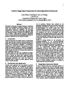
Aim of the flow presented in this work is to generate the low-level implementation of the desired system in order to make it possible to physically configure the target device to realize the original specification. The flow is divided in three, concurrent, parts: the hardware (HW) side, the reconfigurable (RHW) side and the software (SW) side. A diagram showing the whole process is presented in Figure 1.
4.
THE FLOW: HW AND RHW SIDES
The first steps that must be performed in the HW and RHW sides are the HDL Core Design and the IP-Core Generation. The latter phase extends the cores description with a communication infrastructure that makes it possible to interface them with a bus-based communication channel. After these steps, the static components of the system are synthesized together to realize the static architecture, while the reconfigurable components are handled separately as reconfigurable IP-Cores. In order to implement the correct communication infrastructure between the static component and the reconfigurable ones, the component placement constraints need to be known. Therefore, before the generation of the HDL description of the overall architecture the placement constraints phase must be executed.
4.1
System Description Phase
The first phase of the flow consists in the creation of all the necessary files used to describe the reconfigurable system. This phase accepts as input the VHDL descriptions of the core logic used to implement the desired application and the system description file containing the information regarding the overall solution (i.e. the number of reconfigurable slots, the need of the runtime relocation support). It is possible to identify four different set of files used to describe the corresponding four basic architecture components: the reconfigurable side, the static side, the communication infrastructure and the overall system architecture. The system description phase has been organized into four different subsequent steps: the IP-Core generation and the system architecture generation, described below.
4.1.1
The IP-Core generation
Aim of this phase is to build complete IP-Cores from their core logic. This task is automatically performed through a tool [33] which performs three steps: registers mapping, address spaces assignment and signals interfacing. The registers mapping step is needed because each core may have different (number, type, size) set of signals, therefore this phase creates the correct binding between the register defined in the core logic and the one that have to be created inside the new IP-Core. During the second step each register, mapped to a standard signal, is assigned to a specific address, allowing addressing a specific register through the address signals. In the last step target bus signals are mapped to registers. After the execution of this sequence of steps, the IP-Core is ready to be bound to the target bus and has a proper interface. Experimental results reported in Section 6 show that interface overhead is acceptable, especially when the core size is relevant. The generated IP-Cores will then be provided as input to the Reconfigurable Modules Creator or to the EDK System Creator tools, according to their nature, static or reconfigurable, as defined in the system characterization file.
4.1.2
System architecture generation
Once the IP-cores are ready, the system architecture generation can start. Since the basic structure of a self reconfigurable architecture is made of two different parts (a static part and a reconfigurable one), there are two tools in charge of creating these portions: the reconfigurable modules creator accepts as input the reconfigurable IPcores and it provides as output the VHDL description of the corresponding reconfigurable modules. The static system
Figure 1: The enhanced Caronte design flow overview creator takes as inputs the base EDK-architecture used to define the core of the static side and the static IP-cores. The
static system creator provides as output the description of the whole static part.
The next two stages of the System Description phase come after the Design synthesis and Placement Constraints Assignment phase, because they required placement information regarding the layout of the overall architecture. The communication infrastructure creator tool takes as input the placement constraints identified by the design synthesis and placement constraints assignment phase and the information regarding the communication protocol that has to be implemented and it provides as output the corresponding macro-hardware used to implement the communication infrastructure. Finally, the architecture generator creates the VHDL description of the top architecture where the static component, the communication infrastructure and the necessary reconfigurable components are instantiated. Experimental results have shown that the most time consuming stages are the static system creation stage and the architecture generation stage. Table 1 reports the results of a set of experiments where the static side of the architecture has been designed using two different processors: the PowerPC 405 and the Xilinx Microblaze. The first column reports the main characteristics of the static part of architecture under test. For example VP7MB1 means that the target FPGA chosen to implement the final solution is the Xilinx Virtex II Pro 7 (VP7) and that the processor instantiated in the static side was a Xilinx Microblaze. Suffixes 1 and 2 characterize different static architectures, where different means that they have been defined using different sets of IP-Cores. Table 1: Static Part Time Requirements
VP7MB1 VP7MB2 VP7PPC1 VP7PPC2 VP20PPC1 VP20PPC2 V4MB1 V4MB2
4.2
Parsing (ms) % 13981 44 16489 41 21339 47 22262 41 15413 42 17292 42 11631 42 13642 38
Static (ms) % 13666 43 16490 41 18989 42 22901 43 16533 45 16898 41 11915 43 14755 42
Top (ms) 3783 6776 4964 8476 4841 7135 3937 6989
% 12 17 11 16 13 17 14 20
Design synthesis and Placement Constraints Assignment Phase
Aim of this phase is the definition of the placement constraints such as the position of the reconfigurable slots or the physical location of bus-macros.
4.2.1
Design Synthesis
This stage is used to synthesize each system module in order to estimate the resources that will be required to define the corresponding configuration code.
4.2.2
Floorplanning Reconfiguration Driven
This stage defines the area constraints for each configuration code. Since to every configuration code are associated the corresponding resource constraints computed during the design synthesis phase, it is possible to identify a floorplanning constraint that take into consideration both the re-
source requirements and the constraints introduced by the reconfigurable scenario (i.e. working with a Xilinx device, a width constraint multiple of 4 slices [3, 4]). Hence the floorplanning reconfiguration driven stage provide as output an area constraint aware of all the constraints introduced by the reconfiguration scenario.
4.2.3
Placement Constraints
Aim of this stage is the identification of the placement constraints that will be used to implement each configuration code. The floorplanning reconfiguration driven stage provide a set of feasible area constraints, but the problem that still needs to be solved is the identification of the placement constraints taking into consideration the fact that those configuration codes are not configured as single core on the reconfigurable device, but they have to share the reconfigurable resources with other configuration codes. The UCF Builder and Analyzer (BUBA) tool takes as input the starting area solutions computed by the previous stage, a static scheduling of the application and the information regarding the reconfigurable device that has to be used to implement the desired design. All this information is provided in the system characterization file. Due to these parameters BUBA assigns, using a greedy algorithm, the placement constraints to each module trying to minimize the number of reconfigurations [34]. This is possible due to the fact that a module can be executed at different times and not only once. In such a scenario there might be a placement solution able to keep configured a configuration code on the reconfigurable device, without affecting the quality of the schedule, without having to reconfigure the same module twice or more just because it is no longer available on the reconfigurable device. Once the new placement constraints are defined these information are stored into the system characterization file and into the UCF file and provided respectively to the system architecture generation stage in the System Description phase to implement the correct communication infrastructure and to the context creation stage in the System Generation phase.
4.3
System Generation Phase
The previous two phases produce all the necessary files (i.e. HDL descriptions, UCF file, macro-HW definitions, etc) describing the desired system. The last phase of the flow is the System Generation phase. It can be used to support both Xilinx EAPR [4] and Module-based [3] reconfigurable architecture design flows. This phase is divided in two different stages: the Context Creation and the Bitstream Generation.
4.3.1
Context Creation
The Context Creation phase is organized into three different stages: Static Side Implementation, Reconfigurable Modules Implementation and Context Merging. The first one accepts as input the HDL files2 generated during the system description phase and the placement information defined via the design synthesis and placement constraints assignment phase. Aim of this stage is the physical implementation of the static side of the final architecture. The placement information of this component will be provided as input to the Context Merging phase of the final architecture. A second output, working with the EAPR flow, is represented by the information of the static side components 2
NMC and NGC files
that are placed into the reconfigurable modules region (i.e. routing, CLBs usage). The Reconfigurable Modules Implementation stage needs as input the placement information for each module and the corresponding VHDL files defined during the previous two phases. This stage defines the physical implementation of each reconfigurable component. It is composed by three different steps: the NGDBuild, the mapping and the final place and route stage. The Reconfigurable Modules Implementation stage needs to be executed for reconfigurable component. Finally, the Context Merging stage produces as result the merging of the outputs produced by the two previous stages.
4.3.2
THE FLOW: SW SIDE
A dynamic reconfigurable architecture often needs software integration to control the scheduling of the reconfiguration. This kind of tasks can be implemented either as a stand-alone software application or through an Operating System (OS) that provides reconfiguration mechanisms. In the proposed methodology the latter method is chosen, since it is more flexible and powerful. The first steps that must be performed in the SW side are the development of a reconfiguration control application and the development of a set of drivers to handle both the reconfigurable and the static components of the system. All these software applications are compiled for the processor of the target system. The compiled software is then integrated, in the Software Integration phase, with the boot-loader, with the Linux OS and with the Linux Reconfiguration Support (LRS). The LRS extends a standard Linux OS by adding support for PLDs full and partial dynamic reconfiguration. Once the bitstreams created by the Bitstreams Generation phase are available, the last step of the proposed flow can be performed. It is called the Deployment Design phase, it generates the final solution, which is made by the initial configuration bitstream, the partial bitstreams, the software part (boot-loader, OS, Reconfiguration Support, drivers and controller) and the deployment information that will be used to physically configure the target device.
6.
4-input luts 30 172 64 339 15 146 273 308 4124 4314 1028 848 1750 2089
Perc. 0% 2% 1% 4% 1% 1% 2% 3% 42% 44% 10% 9% 18% 21%
Occupied Slices 26 122 37 205 11 103 153 173 2132 2250 913 940 950 1079
Perc. 1% 2% 1% 4% 1% 2% 3% 3% 43% 46% 18% 19% 19% 22%
Time (s) 0.049 0.053 0.045 0.058 0.075 0.063 0.071
Bitstream Generation
The last stage, Bitstream Generation, creates a complete bitstream of the top architecture that configures the system and a set of empty modules. Then for each module two partial bitstreams have to be created: one is used to configure it over an empty module and another one to restore the empty configuration.
5.
Table 2: IP-Core generator tool tests IP-Core Core: Mult1 IP-Core: Mult1 Core: Mult2 IP-Core: Mult2 Core: IrDA IP-Core: IrDA Core: FIR IP-Core: FIR Core: AES128 IP-Core: AES128 Core: RGB2YCbCr IP-Core: RGB2YCbCr Core: Complex ALU IP-Core: Complex ALU
EXPERIMENTAL RESULTS
This section presents different examples to prove the effectiveness and the quality of the proposed methodology. Tables are not exhaustive for conciseness reasons; they report results concerning only the most interesting phases. Table 2 presents some results relative to the tool used during the IP-Core generation phase. The set of tests is composed by several types of components, starting from simple core like IrDA interface to more complex core such as Complex ALU. For each test the table shows the resource needed by the logic core and by the generated IP-core in terms of 4-input LUTs and slices. Also, the table shows the completion time for every test, which is almost constant and on the average is of 0.065 seconds.
To validate the subsequent phases of the flow, different examples have been developed. Aim of those examples is to prove that the proposed flow is not only platform independent but it can be used to design different reconfigurable architectures, adopting internal or external reconfiguration; it is processor-independent (i.e., PowerPC or Microblaze) and it can work with different reconfigurable constraints (i.e., the 1D for the Virtex and Spartan FPGAs and the 2D for the Virtex4 devices). The target device of the first two examples is a Virtex-II Pro VP20 FPGA, integrated in an Avnet Evaluation Board; the first example relies on a Microblaze soft-processor implemented in the static part of the design. The second example is based on the PPC 405 hard-processor embedded into the FPGA. The target device of the last two examples is a Virtex-4 FX12 FPGA mounted on a Xilinx Development Board; as for the previous case, the two examples are based respectively on a soft-core and on a hard-core. The number of reconfigurable slots used for every example is four. Furthermore, in all examples, the reconfigurable and the static regions have been submitted to several tests in which their size has been incrementally decreased, in order to achieve different shapes for each one of them. The approach proposed in this paper has been applied to automatically develop several reconfigurable architectures. All these architectures have been successfully tested on the target devices. The latency of the whole architecture mainly depends on the hardware reconfiguration latency, which is directly proportional to the size of the requested module. Several cores, spanning from simple functional units to more complex ones such as RGB converter, FIR (the last two have been used as part of a complete edge detector system), have been implemented as reconfigurable components. Their size span from 113 slices for a simple squarer to 4314 slices for an AES128 module. What determines the latency, however, is the number of CLB columns that must be reconfigured. This number is varied, during the tests from 1 column to 12 columns.
6.1
A complete application
In this section it is described a complete application typical of the Image Processing area. Several applications in this domain are characterized by data intensive kernels that involve a large number of repetitive operations on input images. These kernels can be implemented on PLDs, since computational intensive tasks are mapped onto the reconfigurable hardware. The application chosen to validate the overall solution is the edge detection problem, computed on sequential frames.
The edge detector used in these experiments is the Canny edge detector, which is composed by four main blocks: image smoothing (fa ), gradient computation (fb ), non-maximum suppression (fc ) and finally the hysteresis threshold (fd ).
Figure 2: Canny edge detector execution model. The model adopted is similar to the one proposed in [35]. The idea is to iterate the execution of each module a certain number of times, and in order to obtain modules whose running time is comparable to the reconfiguration time of other modules, thus hiding reconfiguration overhead, as shown in Figure 2. The image smoothing (FIR) phase is necessary to remove the noise from the image. The image gradient, computed by applying the filter function with a window-approach, is used to highlight regions with high spatial derivatives. Next, the intensity value image and the direction value image, are computed during the nonmaximum suppression stage. At this point it is obtained an image with approximate edges detected, which are often corrupted by the presence of false-edges. In order to delete these non-edges the gradient array is now further reduced by hysteresis. The most computationally expensive parts of the system are the image smoothing filter (FIR), the image gradient and the hysteresis. These functions have been implemented in VHDL and they have been plugged into the self reconfigurable architecture. The resulting system is composed of four modules. The distribution of the application functions into these modules is presented in Table 3. Table 3: Modules partitioning. Tasks m1 m2 m3 m4
Application Functions Static Side, non-maximum suppression fc image smoothing (FIR) fa gradient fb hysteresis fd
Occupied Slices 2662 245 2168 5343
Percentage 54 4 44 108
Module m1 contains the static side, i.e., the PowerPC core and all the interface infrastructures as well as the function fc (non-maximum suppression). The other three tasks correspond to one IP-Core implemented with reconfigurable hardware. The resource requirements of these IP-Cores are shown in last two columns of Table 3. As a result, m1 is extended to support both fc (non-maximum suppression) and fd (hysteresis). This move does not incur in any additional overhead for the realization of module m1 . Module m1 already contained one application function (fc ). Therefore, necessary computational resources (a PowerPC core) and communication components to correctly interface the software functions with the IP-Cores have already been created and accounted for. The newly added application function fd will also use this existing infrastructure. With this solution, hardware reconfiguration has to be taken into account because the static portion of the architecture, m1 , along with
the two IP-Cores, the FIR Filter, m2 , and the image gradient function, m3 , are not going to fit into the available reconfigurable hardware resources. In order to have an efficient implementation using partial dynamic reconfiguration, enough data must be processed to justify the reconfiguration between the FIR and image gradient cores (368ms). This example has been proposed to present a complete and real application that can be implemented using the flow using a self dynamic reconfigurable architecture. Obviously the same application can be implemented using a bigger FPGA without needing any reconfiguration. Reconfigurable SoCs are particularly powerful platforms for image and video processing and other multimedia applications. These domains provide essential services for many emerging embedded systems i.e. Smart-Transportation and Biomedical architecture. Motion detection, feature tracking, processing on continuous streams are some applications to this end.
7.
CONCLUSION
It has been demonstrated (see Section 6) that the proposed design flow produces working examples of dynamic reconfigurable embedded systems. The implemented system functionalities range from simple counter or squarer to complex operation such as edge detection. Every tool needed by the flow has been realized and tested. However the authors are currently working in order to improve the framework further on, adding the support for a graphical tool like Simulink and for devices produced by other industries.
8.
REFERENCES
[1] Katherine Compton and Scott Hauck. Reconfigurable computing: A survey of systems and software. ACM Comput. Surv., 34(2):171–210, 2002. [2] H. Kalte, M. Porrmann, and U. R¨ uckert. System-on-programmable-chip approach enabling online fine-grained 1D-placement. In Proceedings of the 18th International Parallel and Distributed Processing Symposium (IPDPS) - Reconfigurable Architectures Workshop (RAW), Santa F´e, New Mexico, 2004. IEEE Computer Society. [3] Xilinx Inc. Two Flows of Partial Reconfiguration: Module Based or Difference Based. Technical Report XAPP290, Xilinx Inc., September 2004. [4] Xilinx Inc. Early Access Partial Reconfiguration Guide. Xilinx Inc., 2006. [5] P. Sedcole, B. Blodget, T. Becker, J. Anderson, and P. Lysaght. Modular dynamic reconfiguration in virtex fpgas. Computers and Digital Techniques, IEE Proceedings-, 153(3):157–164, 2006. [6] B. Blodget, S. McMillan, Brandon Blodget1, E. Keller P. J. Roxby, and P. Sundararajan1. A self-reconfiguring platform. Field Programmable Logic and Applications, pages 565–574, 2003. [7] A. Donato, F. Ferrandi, M. D. Santambrogio, and D. Sciuto. Operating system support for dynamically reconfigurable soc architectures. In 7th International Symposium on System-on-Chip, pages 235–238, 2005. [8] Brandon Blodget, Philip James-Roxby, Eric Keller, Scott McMillan, and Prasanna Sundararajan. A Self-reconfiguring Platform. In Peter Y. K. Cheung, George A. Constantinides, and Jos´e T. de Sousa,
[9]
[10]
[11]
[12]
[13]
[14]
[15]
[16]
[17]
[18]
[19]
[20] [21] [22]
editors, Proceedings of the Field Programmable Logic and Application, 13th International Conference, FPL 2003, volume 2778 of Lecture Notes in Computer Science. Springer, 2003. Christoph Steiger, Herbert Walder, and Marco Platzner. Operating systems for reconfigurable embedded platforms: Online scheduling of real-time tasks. IEEE Trans. Computers, 53(11):1393–1407, 2004. Michael Ullmann, Michael H¨ ubner, Bj¨ orn Grimm, and J¨ urgen Becker. An fpga run-time system for dynamical on-demand reconfiguration. In Proc. of the 18th International Parallel and Distributed Processing Symposium, 2004. J. R. Hauser and J. Wawrzynek. Garp: A MIPS Processor with a Reconfigurable Coprocessor. IEEE Symposium on FPGAs for Custom Computing Machines, 1997. H. F. Silverman. Processor reconfiguration through instruction-set metamorphosis. IEEE Computer, March 1993. Seth Copen Goldstein, Herman Schmit, Mihai Budiu, Srihari Cadambi, Matt Moe, and R. Reed Taylor. Piperench: A reconfigurable architecture and compiler. In Computer, volume 33, pages 70–77, 2000. Ming-Hau Lee, Hartej Singh, Guangming Lu, Nader Bagherzadeh, Fadi J. Kurdahi, Eliseu M. C. Filho, and Vladimir Castro Alves. Design and implementation of the morphosys reconfigurable computing processor. In J. VLSI Signal Process. Syst., volume 24, pages 147–164, 2000. Markus Koester, Heiko Kalte, and Mario Porrmann. Task placement for heterogeneous reconfigurable architectures. In Proceedings of the IEEE 2005 Conference on Field-Programmable Technology (FPT’05), 2005. Heiko Kalte and Mario Porrmann. REPLICA2Pro: Task relocation by bitstream manipulation in Virtex-II/Pro FPGAs. In Proc. of the ACM International Conference on Computing Frontiers, 2006. Edson L. Horta, John W. Lockwood, and David Parlour. Dynamic hardware plugins in an fpga with partial run-time reconfigurtion. pages 844–848, 1993. Hartej Singh, Guangming Lu, Eliseu Filho, Rafael Maestre, Ming-Hau Lee, Fadi Kurdahi, and Nader Bagherzadeh. Morphosys: case study of a reconfigurable computing system targeting multimedia applications. In Proceedings of the 37th conference on Design automation (DAC00), pages 573–578. ACM Press, 2000. David E. Taylor, John W Lockwood, and Sarang Dharmapurikar. Generalized rad module interface specification of the field programmable port extender (fpx). Washington University, Department of Computer Science. Version 2.0, Technical Report, January 2000. Xilinx Inc. Virtex-5 user guide. Technical Report ug190, Xilinx Inc., February 2007. Xilinx Inc. Xilinx Inc. Heiko Kalte, Mario Porrmann, and Ulrich Ruckert. A prototyping platform for dynamically reconfigurable
[23]
[24] [25] [26]
[27]
[28]
[29]
[30]
[31]
[32]
[33]
[34]
[35]
system on chip designs. In Proceedings of the IEEE Workshop Heterogeneous reconfigurable Systems on Chip (SoC), 2002. Alberto Donato, Fabrizio Ferrandi, Marco D. Santambrogio, and Donatella Sciuto. Exploiting partial dynamic reconfiguration for soc design of complex application on fpga platforms. In IFIP VLSI-SOC 2005, 2005. Xilinx Inc. Development system reference guide. Xilinx Inc., 2005. Xilinx Inc. Virtex-4 user guide. Technical Report ug70, Xilinx Inc., March 2007. Fabrizio Ferrandi, Massimo Morandi, Marco Novati, Marco D. Santambrogio, and Donatella Sciuto. Dynamic reconfiguration: Core relocation via partial bitstreams filtering with minimal overhead. In International Symposium on System-on-Chip 06, 2006. H. Kalte, G. Lee, M. Porrmann, and U. R¨ uckert. Replica: A bitstream manipulation filter for module relocation in partial reconfigurable systems. In The 12th Reconfigurable Architectures Workshop (RAW 2005), 2005. Gerard Habay Philippe Butel and Alain Rachet. Managing partial dynamic reconfiguration in virtex-ii pro fpgas. Xcell Journal Online, 2004. Christophe Bobda, Ali Ahmadinia, Kurapati Rajesham, Mateusz Majer, and Adronis Niyonkuru. Partial configuration design and implementation challenges on xilinx virtex fpgas. ARCS Workshops, pages 61–66, 2005. Andreas Weisensee and Darran Nathan. A self-reconfigurable computing platform hardware architecture, 2004. Ewerson Carvalho, Ney Calazans, Eduardo Briao, and Fernando Moraes. Padreh: a framework for the design and implementation of dynamically and partially reconfigurable systems. In SBCCI ’04: Proceedings of the 17th symposium on Integrated circuits and system design, pages 10–15, New York, NY, USA, 2004. ACM Press. V. Rana, M. D. Santambrogio, and D. Sciuto. Dynamic reconfigurability in embedded system design. In IEEE International Symposium on Circuits and Systems, pages 2734–2737, May 2007. M. Murgida, A. Panella, V. Rana, M. D. Santambrogio, and D. Sciuto. Fast ip-core generation in a partial dynamic reconfiguration workflow. In 14th IFIP International Conference on Very Large Scale Integration - IFIP VLSI-SOC, October 2006. M. Giorgetta, M. D. Santambrogio, P. Spoletini, and D. Sciuto. A graph-coloring approach to the allocation and tasks scheduling for reconfigurable architectures. In 14th IFIP International Conference on Very Large Scale Integration - IFIP VLSI-SOC, October 2006. R. Maestra, F.J. Kurdahi, M. Fernandez, R. Hermida, N. Bagherzadeh, and H. Singh. A framework for reconfigurable computing: Task scheduling and context management. IEEE Transaction on Very Large Scale Integration (VLSI) Systems, 9(6):858–873, December 2001.