ulator, routing tools, compilers, hardware configuration and debug- ging tools, application development libraries, and software implementations for hardware ...
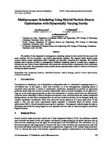
A Multiprocessor DSP System Using PADDI-2 Roy A. Sutton1, Vason P. Srini2, Jan M. Rabaey1 University of California, EECS Dept., Berkeley Data Flux Systems Inc.
CR Descriptors: B.7.1 [Integrated Circuits]:Types and Design Styles - VLSI; C.1.2 [Processor Architectures]:Multiple Data Stream Architectures - Parallel processors; D.1.3 [Programming Techniques]:Parallel Programming; I.3.1 [Computer Graphics]:Hardware Architecture; I.4.3 [Image Processing]:Enhancement.
1 INTRODUCTION We have constructed a system built around a custom parallel DSP chip, PADDI-2[1] (Programmable Arithmetic Devices for high speed DIgital signal processing[2]). The system consists of a multiprocessor DSP board, a host interface controller, and a complete software infrastructure for mapping, configuring, and accessing the board. The host interface controller is in-circuit reconfigurable and is synthesized from VHDL. An algorithm is mapped to the multiprocessor hardware and is also coded completely in software for verification. The hardware and software implementations operate on a single data set and the result is compared. Numerous software tools have been developed to assist in mapping DSP algorithms to the hardware and for verifying the result. The process of mapping an algorithm to the hardware begins University of California, EECS Dept., Berkeley, CA 947201 Data Flux Systems Inc., 1678 Shattuck Ave., MS 292, Berkeley, CA 947092 This project is partially funded by USAF, Eglin AFB, FL under the contracts F08630-94-C-0074 and F08630-95-C-0101. Additional support comes from a Lucent Technologies/Sandia National Laboratories CRFP Fellowship. th
2 HARDWARE PADDI-2 A goal of PADDI-2 is to achieve high performance (billions of operations per second) by interconnecting numerous simple processors in an MIMD fashion. It is intended for signal processing applications that contain abundant parallelism[3][4][5]. It’s architecture draws on ideas from earlier architectures[4][6][7][8][9]. chip i/o cluster-11
We have integrated an image processing system built around PADDI-2, a custom 48 node MIMD parallel DSP. The system includes image processing algorithms, a graphical SFG tool, a simulator, routing tools, compilers, hardware configuration and debugging tools, application development libraries, and software implementations for hardware verification. The system board, connected to a SPARCstation via a custom Sbus controller, contains 384 processors in 8 VLSI chips. The software environment supports a multiprocessor system under development (VGI-1). The software tools and libraries are modular, with implementation dependencies isolated in layered encapsulations.
with manual partitioning using a graphical SFG entry tool. The partitioned algorithm is then simulated and routed using another graphical tool. The result is then compiled to a configuration bitstream, downloaded to the multiprocessor board, and run using configuration and I/O tools. The board software is built upon an application programming interface and driver library. The software has been designed in a modular manner to facilitate compilation under other computer operating systems and to reduce the dependence on PADDI-2. Implementation details have been encapsulated in replaceable software libraries. There are three custom hardware component types: a parallel DSP processor (PADDI-2), the multiprocessor system board, and a computer interface controller.
level-2
cluster-0
ABSTRACT
level-1 in clusters
As shown above, it is a 48 node multiprocessor chip, composed of 12 clusters, each with 4 simple “nanoprocessors.” Two levels of interconnect are present. There are six level-1 data buses and four one-bit control buses within each cluster. These buses are used for local communication within a cluster and for communication from within a cluster to outside a cluster. They extend into a second level crossbar. The level-2 interconnect has 16 data buses and eight one-bit control buses and are used to provide connectivity between clusters. Each nanoprocessors has 17 programmable switches available to make connections to level-1 buses. Clusters have 50 switches within each level-1 to level-2 crossbar. The eight outer most clusters have dual purpose nanoprocessors which provide off-chip I/O. Six general purpose registers, three scratch pad registers, an
35 Design Automation Conference ® Copyright ©1998 ACM 1-58113-049-x-98/0006/$3.50
DAC98 - 06/98 San Francisco, CA USA
eight element instruction memory, and a simple control unit is present within each nanoprocessor. All instructions have a single cycle latency with branches delayed by one cycle. A two stage pipeline is used. The processor implements 12 instructions including: add, add with carry-in, subtract, subtract with carry-in, logical or, logical and, logical xor, logical invert, arithmetic up shift, arithmetic down shift, booth multiply, and select. Multiplication can be done in eight cycles on a single processor or eight processors can be pipelined to deliver a result every cycle. The add and subtract with carry-in instructions allows data precision in multiples of 16. Each processor fetches instructions from its eight-word instruction memory. Data may come from internal registers or external sources via two-word input queues (the registers of the processor can be configured as upto three queues). The execution of all the processors can be halted via global control. Data communication between all processors, irrespective of position, takes one cycle and uses a hardware synchronization handshake protocol. With each clock cycle, handshake lines are precharged. If a sender or receiver is not ready, it is pulled low (wired or). This will stall all participants. The line will remain charged if, and only if, all participants are ready to pass a data token. This mechanism eliminates the need for global synchronization and retiming during the mapping process. PADDI-2 has a 7464-bit scan chain that traverses the die, providing static configuration for each programmable resource, including the processors and interconnect. In addition to configuration loading, the scan chain is also used for debugging. After a global halt, the status of each processor can be retrieved and examined under global control. PADDI-2 has been fabricated using a 0.8 micron CMOS process with two levels of metal. The die size is 11.5 mm X 11.5 mm and is housed in a 208 pin ceramic package. Additional details can be found in Yeung’s Ph. D. thesis [1].
connected to an external memory. Two ports are used to send and receive data to and from the host interface controller via a private 16-bit data bus. Address generation and read write control for the memories is performed under nanoprocessor control. This provides flexible memory access. One common access method is the delay line mode. Another example, which demonstrates this flexibility, is a multiple delay line implemented using one physical memory. The address generator requires 6 instruction lines using the nanoprocessor instruction set. A board design goal was to demonstrate and evaluate the efficiency and flexibility of PADDI-2. At 50 MHz, each board can provide 20 GOPS of computation. It is being used to explore PADDI-2’s architecture, its strengths and weaknesses, so as to provide guidance in our next generation architecture.
Host Computer Interface Controller The multiprocessor board is connected to a workstation using a custom interface controller. It has two main components: a field programmable gate array and a host bus-interface chip. We have designed an adapter for the Sun Microsystem SBus. The low level SBus protocol is implemented using an LSI L64853A interface chip. Global control is implemented using a field programmable gate array (Xilinx 4010) and is in-host reconfigurable. Its purpose is three fold. It realizes the protocol translation between the SBus interface chip and the private bus. It performs arbitration for the private bus. And, it provides global control for the processors. The FPGA controller logic is specified using VHLD and is synthesized. This enables us to explore alternative protocols, arbitration schemes, and global control techniques without re-fabricating hardware. Mature controller realizations (configuration bitstreams) are cataloged for reuse.
Multi-processor DSP board Multiple PADDI-2 chips have been integrated within a testboard. This board has eight independent chips, each with a 128KB static RAM. The interconnection of the I/O between chips is hardware configurable via jumpers. Each chip can be configured to connect one or more ports to its four logical neighbors in a 4x2 torus fashion. Multiple boards can be daisy chained into a single logical device and connected to one host adapter. Since synchronization is done locally in hardware, this method of scaling works well. Alternatively, additional interface controllers, with one or more multiprocessor boards can be added to increase available computation. System software has been implemented to address any number or configuration of boards. Port connectors are provided to facilitate “plug-in” daughter-card and peripherals such as sensors, displays, and other devices.
3 SOFTWARE The software components of the system can be classified into eight general types. These type are identified in the table below and each is discussed in the following sections. Software Libraries in Java (High-level Validation) SFG Graphical Interface (Visual Entry and Manipulation) Routing Tools (Interactive/Automatic PR) Simulation Tools (Functional Verification) Compilation Tools (Instruction Stream Configuration) Board Access Tools (Communication with Hardware) Board Debugging Tools (Interrogation of Hardware Status) Development Libraries (Tools Development Libraries)
Development Libraries
Due to the wide variation in communication requirements for the algorithms of interest, no single optimal interconnect topology exists. Our approach is to provide board-level options for interconnect configuration over a common range. In the configuration shown above, the chips are connected in serial fashion with each
A set of application development libraries has been implemented. Six libraries have been developed to provide standard interfaces upon which other tools are built. A low level I/O, a link level I/O, a scan chain bit manipulation, a controller access, and a general purpose parsing package have been developed. These packages provide non-overlapping function and interact in a layered fashion. If any hardware component changes, only those libraries directly affected by the change need to be modified. For example, if we were to replace PADDI-2 with VGI-1 in the existing multiprocessor board, only the scan chain manipulation library would need modification.
Board Debugging Tools Several utilities have been written to provide parameterized stimulation of all hardware components. For example, to verify that the chip scan chains are operational, a utility has been written that generates test vectors. It can provide numerous, in type and quantity, test patterns for a variable number of boards and chips. As a second example; one of the interface controller configurations supports parameterizeable timing. When this version is used to configure the interface controller, a test tool is available to dynamically modify various controller timing parameters. This was used to optimize controller efficiency and function. Numerous other debugging tools exist, but will not be described.
Board Access Tools Four major board access tools have been developed. One is used to download the configuration bitstreams to the FPGA in the interface controller. A second is used for configuration of the PADDI-2 processor array. The third is used to provide I/O streams to algorithms running on the array. A fourth exists which helps debug algorithms that use external data memory. The tools all have a “self documenting” command line which provides a usage synopsis. It provides command description, revision, argument keywords, argument keyword data types, argument descriptions, and argument defaults, when run with no options. All tools can be readily invoked within scripts and other programs to perform complex sequences.
Compilation Tools To compile an algorithm, one writes assembly code for each function in the signal flow graph. These instruction streams are assigned to specific nanoprocessors within a chip using an index file. This is also where the level-1 and level-2 interconnect is configured. All switches are, by definition, off and are explicitly turned on as needed. A separate index is created for each chip used in an algorithm. The compilation tools generate configuration bitstreams for a chip. Each assembly file is compiled by the assembler (asm) to an intermediate object file. A netlist is generated from the index (gen_vsm). This netlist and intermediate object files are combined (pgen) to generate the chip configuration bitstream. This process is ordered by a makefile which itself can be automatically generated (mkmf_set). This is required for each chip on a board. Chip configuration bitstreams are assigned to physical chips using a metaindex file. This file simply is an index which relates chip configurations to chip numbers. A makefile is also used hierarchically to ensure that each chip configuration is current. This makefile can also be automatically generated (mkmf_mset). The entire source for an algorithm can be built using a single call to make on the metaindex makefile.
Simulation Tools A functional simulator has been developed to assist in application development. The simulator is written in Java for portability. It processes compiled assembly code to initialize the simulated chip state. A nanoprocessor simulator is instantiated for each assembled object used in the index file. The index file is also used to establish the communication interconnections between instances. The simulator, like the hardware, can be run, halted, and stepped. At any time the processor state can be viewed. All register, queue, output port, condition code, flag register, current pc, previous pc, and next pc, and processor stall information is available. The state of each nanoprocessors is summarized in separate state windows and nanoprocessor communication can be observed and recorded. Chip I/O is also simulated. With this, the same data sets processed by the hardware can also be processed by the simulator.
VGI-1 has on-chip data memory and independent I/O processors. Extensions to support these and the other additional function are under development. The implementation organization is general enough to support similar designs which use hardware synchronization to communicate between processors. The network primitives support arbitrary hierarchical networks topologies with programmable routing.
Routing Tools One of the more difficult tasks in programming multiprocessor systems (of this class) is establishing the required inter-processor communication. To assist, a graphical routing assistant tool has been developed which performs the allocation as a user requests and assigns routing resources. The interconnect network is constructed from a specification data set which describes the resource available on the chip. The algorithm index file is read to identify nanoprocessor instruction sequences. Nanoprocessor assignment and interconnect resources are interactively allocated graphically. The assistant keeps track of all available and allocated resources. Routes are allocated from a displayed list of available routes computed based on a user selected processor pair. Previously allocated resources can be released and reallocated in any order. We have a slow tool for automated PR which is guaranteed to find a mapping, if one exists, by using exhaustive methods.
SFG Graphical Interface A graphical signal flow graph manipulation tool has been developed to help in algorithm mapping and visualization. SFG's are represented using nodes, edges, and graph objects. All objects accept arbitrary property tagging (selectably visible or invisible) and support hierarchical composition. For example, a node can contain other objects, such as another graph, or collection of graphs. Nodes may be moved around at will, grouped into clusters (subgraphs) and collapsed into a single node. This tool aids in interactive SFG partitioning, manual placement, and routing. It works in conjunction with the other mapping tools by sharing a common I/O data representation. A SFG can be interactively partitioned, placed, and routed with this tool. One selects groupings which can be mapped to clusters, assigning properties to the nodes and edges to allocate level-1 resources. Next groupings are assigned to clusters by adding properties to the higher-level node which contains the grouped subgraphs. Finally, properties are added to the edges which interconnect groupings to allocate the required level-2 routing resources. Alternatively, a partial mapping can be obtained from other tools, such as the slow autorouter, and completed manually by visually identifying the objects which have not been assigned (those missing an assignment property).
Software Libraries in Java for Image Processing Our algorithm mapping flow has two paths which branch from the algorithm and re-converge with an algorithm input data stream. One which targets hardware realizations and another which targets software realizations. This algorithm-in-software path provides system level verification of algorithm-in-hardware mappings. The output of both implementations is compared and differences are readily observed. A subtraction of one image from the other is one such useful comparison. Several image processing algorithms have been implemented. Enhancement algorithms include median filters, local averaging, max/min sharpening, and blurring filters. For edge detection, we have the discrete differencing, the Robert’s edge detector, the Prewitt edge detector, and the Sobel edge detector. Others include the fast fourier transform and the inverse transform. Others, such as
the discrete cosine transform and wavelet transform, are under development.
4 SYSTEM USAGE Currently the task of going from algorithm function to nanoprocessor assembly code is manual, and uses macro libraries, however, techniques are being investigated to support more automated mapping flows. Given the simplicity of a nanoprocessor, code generation is not difficult. The processor assembly code, node-to-processor assignment, and the interconnect routing assignment are processed to produce a configuration bitstream which is downloaded to configure the array. A separate assembly source file is required for each unique node of the SFG. An index is used to map assembly code to nanoprocessors.
A Mapping Technique There are numerous techniques for mapping. The efficiency of the technique chosen is highly dependent on the algorithm description. We assume the algorithm to be described by an SFG and that each node does not exceed the context or port capacity of a nanoprocessors. PADDI-2’s two level interconnect architecture encourages a two phase mapping process; intra-cluster routing, followed by inter-cluster routing. The discussion below is an example of one mapping scheme. The task of intra-cluster routing involves first partitioning then placing and routing subgraphs of the algorithms SFG. Node count, port count, and interconnect topology limits the selection of subgraphs. Once all nodes of the algorithms’ signal flow graph have been assigned to a subgraph, this phase is complete. The routing resource within a cluster is shared to provide internal and external I/O. For example, a level-1 bus can be used to connect two nodes within the cluster or it can be used to connect a node within a cluster to one outside the cluster. Because of this, there is a dependency between intra- and inter-cluster routing. In some cases, intra-cluster routing obstructs inter-cluster routing and in these cases, one might identify alternative intra-cluster routing to avoid such obstructions. An obstruction is not revealed until the second routing phase. In the second phase, groupings are assigned to clusters and interconnected as required by the partitioned SFG. This involves assigning subgraphs to clusters and allocating level-2 interconnect resources for the inter-cluster communication. Once all subgraphs have been assigned and interconnected, then mapping is complete.
5 SUMMARY We have integrated a complete DSP system built around PADDI-2. This hardware/software design consists of a DSP, system boards, driver libraries, access tools, configuration tools, algorithm development tools, and verification software. We have produced a flexible functional simulator which works for both PADDI-2 and VGI-1 and provides routing and placement assistance in a Java based graphical tool. Our software development libraries have been designed for portability. New board configurations and hosts environments can be supported with minimal porting effort. Our multiprocessor DSP array has been designed to be modular and scalable and can directly incorporate sensor daughter cards. Several innovations exist in the PADDI-2 chip architecture. A flexible interconnect switch has been designed which requires approximately 17% the die area. Additionally, a robust hardware local synchronization technique has been implemented which reduces programming difficulties present in many other multiprocessor systems. Consistency was used in the software development
methodology and command utility interfaces. The PADDI-2 chip was designed and verified using the Lager tool set and other VLSI design tools developed at the University of California, Berkeley. The custom boards were designed using Lager in conjunction Racal-Redac’s to describe, place, and route board components. VHDL synthesis is performed using ViewLogic and mapped using XACT. Java programs were developed using JDK. Web formatted code documentation[10] were automatically generated using EXT.
Acknowledgments We would like to acknowledge contributions of other research group members. Arthur Abnous implemented the PADDI-2 assembler. Nelson Chow worked on various parts of the board design and fabrication. Alfred Yeung delivered PADDI-2 an accompanying compiler. Matt Armstrong implemented the Java simulator and routing assistant. Erek Borowski coded numerous software implemented algorithms in Java and the SFG graphical interface. Stas Frumkin assisted with board layout and routing. The help provided by Brian Richards, Fred Burghardt, and Sue Mellers is appreciated. The encouragement and support provided by Bob Brodersen is greatly appreciated. STTR USAF funding is monitored by Robb Brown. The suggestions provided by Pat Coffield are appreciated.
REFERENCES [1] Yeung, A. K. W., “PADDI-2 Architecture and Implementation,” Ph. D. Thesis, University of California, Berkeley, CA, June, 1995. [2] Chen, D. C., “Programmable Arithmetic Devices for High Speed Digital Signal Processing,” Electronic Research Laboratory, Memorandum No. UCB/ERL M92/49, University of California, Berkeley, CA 94720, May 14, 1992. [3] Lee, S. Y. and J. K. Aggarwal, “Parallel 2-D Convolution on a Mesh Connected Array Processor,” IEEE Transactions on Pattern Analysis and Machine Intelligence, vol. PAMI-9, no. 4, pp. 590 -594, July, 1987. [4] Sunwoo, M. H. and J. K. Aggarwal, “Flexibly Coupled Multiprocessors for Image Processing,” 1988 Intl. Conf. on Parallel Processing, St. Charles, IL, Aug. 1988. [5] Webb, J. A., L. G. Hamey, and I. C. Wu, “An Architecture Independent Programming Language for Low-level Vision,” Computer Vision, Graphics, and Image Processing, vol. 37, no. 11, pp. 1751 - 1762, Pittsburgh, PA, Nov., 1989. [6] Stellakis, H. M. and E. S. Manolakos, “A Tri-Array for the Realtime Computation of Higher Order Moment Estimates,” VLSI Signal Processing V, Edited by K. Yao, R. Jain, W. Przytula, J. Rabaey, IEEE New York, pp. 510 - 519, New York, 1992. [7] Robert, M., M. Paindavoine, and P. Gorria, “Architectures for Integration of Real Time Image Processing Systems,” VLSI Signal Processing V, Edited by K. Yao, R. Jain, W. Przytula, J. Rabaey, IEEE New York, pp. 267 - 276, New York, 1992. [8] Intel, “iWARP Forum’91,” iWARP Users Meeting, Crystal City, VA, Sept., 1991. [9] Borkar, S. and et al, “Supporting Systolic and Memory Communication in iWARP,” Proceedings of the 17th International Symposium on Computer Architecture, pp. 70 - 81, Seattle, WA, May, 1990. [10] http://infopad.EECS.Berkeley.EDU/spartan/