is to arrange one analog-to-digital converter (ADC) for each channel. However ... The summation block can be implemented by switched-capacitor (SC) circuits,.
A Single SAR ADC Converting Multi-channel Sparse Signals Wenjuan Guo, Youngchun Kim, Arindam Sanyal, Ahmed Tewfik, and Nan Sun
Abstract—This paper presents a simple but high performance architecture for multi-channel analog-to-digital conversion. Based on compressive sensing, only one SAR ADC is needed to convert multi-channel sparse inputs, leading to significant analog power saving and hardware saving. Moreover, it helps avoid problems occurring in conventional multi-channel ADCs such as timing skew, offset mismatch, and gain mismatch. A 12-bit SAR ADC converting 4-channel sparse signals simultaneously is designed in 130nm CMOS process. The design reaches a SNDR of 66.3dB and consumes an average power of 58µW at the sampling frequency of 1MHz. The L1 minimization method is chosen to reconstruct the input signals. The single-tone and multi-tone inputs can be reconstructed with a minimum precision of 68dB and 55dB THD, respectively.
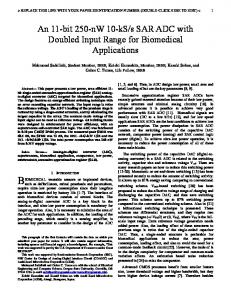
I. I NTRODUCTION The most straightforward way to convert multi-channel data is to arrange one analog-to-digital converter (ADC) for each channel. However, this scheme becomes hardware intensive as the number of channels increases. To reduce the number of ADCs, people tend to use time or frequency multiplexing techniques. In the time multiplexing scheme, all input signals are sampled sequentially. As a result, for a fixed ADC sampling frequency, the bandwidth of each channel decreases with an increasing number of channels, which is undesirable. In the frequency multiplexing scheme, all input signals are modulated to occupy separate frequency bands, thus making the sampling rate of the ADC increase proportionally with the number of channels. A high sampling-rate ADC consumes a large power. This paper presents a way of converting multi-channel data simultaneously with a single ADC sampled at twice the bandwidth of one channel (Nyquist rate). Compared to the conventional approaches mentioned above, the use of one ADC saves the analog power and the hardware cost significantly. Furthermore, it makes our scheme immune to such problems as timing skew, offset mismatch and gain mismatch. The proposed approach is based on the compressive sensing (CS) theory, which requires the input signals to be sparse. The more sparse the input signals are, the more channels the single ADC can deal with, which is detailedly discussed in [1], [2]. In recent years, the CS theory has been exploited in ADC systems to reconstruct a single-channel sparse signal [3], [4], which is different from the multi-channel scenarios investigated in our paper. Fig. 1 gives the overall architecture
978-1-4673-5762-3/13/$31.00 ©2013 IEEE
ADC
Fig. 1.
Reconstruction
Department of Electrical and Computer Engineering The University of Texas at Austin, Austin, Tx, USA, 78712 Email: {wjguo@, youngchun@, arindam3110@mail., tewfik@austin., nansun@mail.}utexas.edu
Proposed system architecture with M channels.
of our proposed scheme. Initially, the input signals are sampled and randomized after multiplying with the pseudo-random binary sequences of plus and minus ones (±1). Next, the sampled values of randomized inputs are summed up. The single ADC converts the summation to digital sequences, from which a reconstruction algorithm separates and restores all channels’ input signals. In this work, the single ADC is chosen to be a SAR ADC for its circuit simplicity, high power efficiency, and scaling compatibility [5], [6]. We effectively integrate the multiplication block, the sample-and-hold (S/H) circuits, and the summation block within the SAR ADC architecture. Our paper also proposes a way to easily expand the number of channels to an exponential value of 2 without additional hardware cost. The paper is organized as follows. Section II explains the operation mechanism of our proposed system and introduces the reconstruction algorithms. Section III presents the detailed circuit implementation of a single SAR ADC capable of converting 4-channel sparse signals simultaneously. Next, Section IV gives the simulation results. Finally, Section V makes the conclusions. II. T HEORETICAL OVERVIEW When we look at conventional ADC techniques exploiting CS [3], [4], the input signals are multiplied with the pseudorandom ±1 sequences in the continuous-time domain, leading to undesirable bandwidth expansion and linearity degradation. The multiplication is followed by an integrator to compute the projections of randomized inputs. By contrast, as shown in Fig. 1, our scheme uses sample-and-hold (S/H) circuits so that the multiplication occurs in the discrete-time domain. Consequently, the projections are also computed in the discrete-time
2235
~xm = Φ~ αm =
N X
αm,n ϕ ~ n,
(1)
n=1
where αm,n is the nth coefficient of ~xm corresponding to ϕ ~ n. th ~rm is the result of ~xm mixed with the m channel PN sequence, p~m ,
A. DAC arrangement The linearity of a SAR ADC system is limited by the digitalto-analog (DAC) capacitor mismatch [7]. To deal with this issue, the whole DAC array is divided into two segments which we call the MSB DAC and the LSB DAC (see Fig. 2). The error induced by the LSB DAC capacitor mismatch is less than the quantization noise so that it is negligible. Therefore, we only need to calibrate the MSB DAC capacitor mismatch. The LSB DAC are used to estimate the mismatch error from the MSB DAC. At the same time, the MSB DAC incorporates a redundant capacitor (26 C) whose value is equal to the summation of all the capacitors in the LSB DAC. This capacitor provides a sufficient redundancy required by the calibration. It also facilitates the sampling of the input signals, for they only need to be sampled on the MSB DAC. The LSB DAC is set to sample Vcm .
data
~rm = p~m ~xm .
calibration
enable 0 1 -1 SAR Logic
(2)
After the multiplication, all the modulated signals are added to give ~s as, ~s =
M X
~rm .
(3)
−
m=1
MSB bp
Plugging (1) and (2) into (3), ~s can be rewritten as,
~s =
M X N X
αm,n (~ pm ϕ~n ) =
m=1n=1
where ψm =
N P
M X
0
ψm α ~ m = Ψ~ α,
(4)
~n , Ψ = [ψ1 , ψ2 , · · · , ψM ], and α p~m ψ ~T =
n=1 T ,α ~M ].
[~ α1T ,~ α2T , · · · As can be seen, Ψ is a known N × W matrix, and α ~ is an unknown W × 1 vector, where W = M N . ~s is measured by the ADC whose output is, d~ = ~s + ~n = Ψ~ α + ~n,
+
0
Fig. 2.
m=1
LSB
ACLK
domain, which means the continuous-time integration process can be replaced by a discrete-time summation. The summation block can be implemented by switched-capacitor (SC) circuits, which are insensitive to process, voltage, and temperature (PVT) variations. Therefore, our scheme also ensures a high linearity. Mathematically speaking, the mth channel input signal, ~xm �RN can be represented as (1) when expanded over the N -point discrete Fourier transform (DFT) basis, Φ�C N ×N . Φ consists of N column vectors, ϕ ~n = √1 exp{−j2πk(n − 1)/N }, where n = 1, 2, · · · , N , and N k = 0, ±1, · · · , ±dN/2 − 1e.
Proposed 4-channel 12-bit SAR ADC.
To calibrate the largest capacitor (211 C), {1,-1,-1,-1,-1,-1,1} are firstly sampled on the MSB DAC. After sampling, we force the MSB DAC connected to {-1,1,1,1,1,1,1}. If there is no mismatch for this capacitor, the comparator’s input voltage should be 0. If there exists mismatch, the comparator’s input voltage is non-zero, which is further converted to a digital sequence by the LSB DAC. Based on the calibration equations in [8], we similarly calibrate other capacitors in the MSB DAC.
(5) 0
where ~n represents the noise induced by the ADC. This is an undetermined equation. To solve this equation, we can apply linear/convex optimization approaches, or greedy approaches [1], [2]. Once α ~ is accurately estimated, the input signals can be reconstructed based on (1). The reconstructed signals are represented as {ˆ xm } in Fig. 1.
MSB bp
LSB
0
III. C IRCUIT IMPLEMENTATION To verify our proposed architecture, a 12-bit SAR ADC capable of simultaneously converting 4-channel sparse signals was designed using 130nm CMOS process. Although the actual design is fully-differential, a single-ended version is shown in Fig. 2 for simplicity. 0,1,-1 represent the commonmode voltage, positive reference, and negative reference, respectively.
Fig. 3.
DAC array for 4-channel 12-bit SAR ADC.
B. 4-channel sampling In the sampling phase, all the inputs are sampled on the MSB DAC while the LSB DAC will sample Vcm . In order to sample 4 channels simultaneously, we halve the largest
2236
Vdd
capacitor (211 C) and evenly distribute the MSB DAC to 4 channels, which is illustrated in Fig. 3. The number of channels can also be extended to any exponential value of 2 by further halving more capacitors. This technique not only saves hardware cost but also avoids the timing-skew problems among channels, for all the channels share the same bottomplate sampling switch (bp) (see Fig. 3). Besides, they also share one comparator, thus avoiding the offset mismatch. Since the gain mismatch is due to the capacitor mismatch, it can be calibrated once the capacitor mismatch is measured as in Section III-A. Following the sampling phase, the summation is completed on-the-fly. Based on charge conservation, we can derive the summation result as,
lat
lat
Vdd
Vdd
lat
lat lat
reset
stop
lat
(a)
s = (r1 + r2 + r3 + r4 )/4.
Vdd
(b)
(6) Fig. 5.
Comparator Schematic: (a) Pre-amplifier. (b) Strong-arm latch.
With respect to (3), there is a scaling factor of 1/4 in (6), which can be easily compensated during reconstruction.
IV. S IMULATION R ESULTS
C. Multiplication
A. Performance of the SAR ADC
The multiplication between a differential signal and a ±1 sequence is equivalent to changing the polarity of the signal. As shown in Fig. 4, we use several switches controlled by the pseudo-random sequences to change the polarity of the input signals sampled on DAC arrays, thus meaning the input signals are multiplied with ±1 in the discrete-time domain. x and x ˜m are the positive and negative end of a differential signal. p˜m is the inverse sequence of pm . rm and r˜m respectively go into the positive DAC array and the negative one.
The ADC’s performance is first tested in SPICE by setting the random sequences {~ pm } to be 1. The sampling frequency is 1MHz. The total capacitance for a single-ended DAC is 1.67pF. The 4 inputs are set to be pure sinusoidal waves with the same amplitude of 2.4V peak-to-peak, and the frequencies of 43kHz, 121kHz, 199kHz, and 277kHz. The output spectra is shown in Fig. 6 whose y-axis limit is set to be [-100, 0]dBFS for the compactness of the figure. Table I shows the noise budget and the SNDR of the ADC. The ADC consumes an average power of 58µW . TABLE I ADC NOISE BUDGET. Sampling noise [µV ] 70
Fig. 4.
QN [µV ] 169
Comp Noise [µV ] 366
Total Noise [µV ] 409
Proposed mixer schematic.
D. Comparator The comparator consists of two stages as demonstrated in Fig. 5. The first stage is a diode-connected pre-amplifier, which provides a gain of 11dB and consumes an average power of 4µW . A reset switch labeled M3 is used to remove the memory-effect in the pre-amplifier. When the data conversion is completed within one period, a stop signal will be asserted at M6 so that the preamplifier will not consume any power when the system is in stand-by. The second stage is an improved strong-arm latch, which is triggered by the lat signal. M10 and M11 are added to reduce the effects of kickback noise. M18 and M19 are used to remove the memoryeffect in the latch.
2237
Fig. 6.
Output spectra of the SAR ADC.
SNDR [dB] 66.3
B. Signal reconstruction The 4-channel conversion capability of the proposed system is further verified by multiplying the input signals with the random sequences {~ pm } and reconstructing them from the output result of the single SAR ADC. Simulations are performed with single-tone and multi-tone input signals, and we compute the total harmonic distortion (THD) of each signal case after reconstruction using the L1 minimization method [1], [2]. In the multi-tone input case, we synthesize four-channel input signals with a random number of frequency components, but the total number of frequency components are limited by the sampling bandwidth B = fs /2, where fs is the sampling frequency [2]. The simulation results are presented in Fig. 7-8. In the single-tone input case, the THDs of the recovered signals are 76dB, 69 dB, 70 dB, and 68 dB, respectively. In the multi-tone input case, the THDs of the recovered signals are 57 dB, 55 dB, 56 dB, and 57 dB, respectively.
(a)
(b) Fig. 8. Recovery of multi-tone input signals in (a) the time domain and (b) the frequency domain. Input and reconstructed signals are illustrated in blue and red lines, respectively.
output of the single SAR ADC, both single-tone and multitone inputs are reconstructed in MATLAB with a minimum precision of 68 dB and 55dB THD, respectively.
(a)
R EFERENCES
(b) Fig. 7. Recovery of single-tone input signals in (a) the time domain and (b) the frequency domain. Input and reconstructed signals are illustrated in blue and red lines, respectively.
V. C ONCLUSION In this paper, we present a single SAR ADC architecture that digitizes 4-channel sparse signals simultaneously. The proposed ADC architecture is designed and verified in 130nm CMOS process. Simulations are performed to show the performance of the proposed system using SPICE and MATLAB. In SPICE simulation, the SAR ADC shows a performance of 66.3dB SNDR and consumes an average power of 58µW at the sampling frequency of 1MHz. From the SPICE simulated
[1] Y. Kim, A. Tewfik, and V. Gowreesunker, “Multi-channel analog-todigital conversion using a single-channel quantizer,” in EUSIPCO 2012, Aug. 2012, pp. 1044–1048. [2] Y. Kim, W. Guo, V. Gowreesunker, N. Sun, and A. Tewfik, “Multichannel sparse data conversion with a single analog-to-digital converter,” Emerging and Selected Topics in Circuits and Systems, IEEE Journal on, vol. 2, no. 3, pp. 470–481, Sep. 2012. [3] M. Mishali, Y. C. Eldar, O. Dounaevsky, and E. Shoshan, “Xampling: Analog to digital at sub-nyquist rates,” Circuits, Devices Systems, IET, vol. 5, no. 1, pp. 8–20, Jan. 2011. [4] X. Chen, Z. Yu, S. Hoyos, B. M. Sadler, and J. Silva-Martinez, “A subnyquist rate sampling receiver exploiting compressive sensing,” Circuits and Systems I: Regular Papers, IEEE Transactions on, vol. 58, no. 3, pp. 507–520, Mar. 2011. [5] C. P. Hurrell, C. Lyden, D. Laing, D. Hummerston, and M. Vickery, “An 18b 12.5mhz adc with 93db snr,” in Solid-State Circuits Conference Digest of Technical Papers (ISSCC), 2010 IEEE International, Feb. 2010, pp. 378–379. [6] W. Liu, P. Huang, and Y. Chiu, “A 12-bit, 45-ms/s, 3-mw redundant successive-approximation-register analog-to-digital converter with digital calibration,” Solid-State Circuits, IEEE Journal of, vol. 46, no. 11, pp. 2661–2672, Nov. 2011. [7] J. L. McCreary and P. R. Gray, “All-mos charge redistribution analog-todigital conversion techniques-part i,” Solid-State Circuits, IEEE Journal of, vol. 10, no. 6, pp. 371–379, Dec. 1975. [8] H. S. Lee, D. A. Hodges, and P. R. Gray, “A self-calibrating 15 bit cmos a/d converter,” Solid-State Circuits, IEEE Journal of, vol. 19, no. 6, pp. 813–819, Dec. 1984.
2238