Journal of Theoretical and Applied Information Technology © 2005 - 2008 JATIT. All rights reserved. www.jatit.org
A VECTOR CONTROLLED INDUCTION MOTOR DRIVE WITH NEURAL NETWORK BASED SPACE VECTOR PULSE WIDTH MODULATOR 1
Rajesh Kumar, 2R. A. Gupta, 3Rajesh S. Surjuse 1 Reader., Department of Electrical Engineering, MNIT, Jaipur, India-302017 2 3
Prof., Department of Electrical Engineering, MNIT, Jaipur, India -302017
Research Scholar, Department of Electrical Engineering, MNIT, Jaipur, India -302017 E-mail:
[email protected] ,
[email protected]
ABSTRACT A neural network based implementation of space vector modulation of a voltage-sourced inverter has been proposed in this paper. Use of ANN based technique avoids the direct computation of trigonometric function (e. g. sine function) as in conventional space vector modulation implementation. The main disadvantages with conventional implementation are, use of any look-up table implies the need for additional memory, interpolation of non-linear functions lead to poor accuracy and thus to increased harmonics in the PWM waveforms, the use of a look-up table and interpolation demands additional computing time that limits the maximum inverter switching frequency. The proposed scheme is simple and straight forward and avoids the direct computation of non-linear functions. This scheme is evaluated under simulation for a variety of operating conditions of the drive system and comparison is made with the conventional method of implementation. Results show improved performance and robustness of the drive system. Keywords: Space Vector Pulse Width Modulation (SVPWM), Modulation Index, Voltage Space Vectors, Kohonen’s Competitive Net.
1. INTRODUCTION PWM control of the inverter switches requires to synthesize the desired reference stator voltage space vector in an optimum manner with the following objectives [1]: • A constant switching frequency fs. • Smallest instantaneous deviation from its reference value. • Maximum utilization of the available dcbus voltages. • Lowest ripple in the motor current and • Minimum switching loss in the inverter. The above conditions are generally met if the average voltage vector is synthesized by means of the two instantaneous basic non-zero voltage vector that form the sector (in which the average voltage vectors to be synthesized lies) and both the zero voltage vectors, such that each transition causes change of only one switch status to minimize the inverter switching loss. It is possible to use a competitive type of ANN [2] which has six output nodes in the
competitive layers. Two of these largest net inputs are the winner nodes which are associated with the two adjacent switching vectors. The second task is to compute the on-times (pulse times) of the adjacent switching vectors. Since the two net values contain information of the position (θ) of the reference voltage vector with respect to the two adjacent switching vectors, it is possible to use these net values for the estimation of the on-times of the switching vectors. The details are discussed in the following sections. Space vector modulation was comprehensively investigated in [3]-[7]. Neural network based space vector PWM is implemented in [8]. Here neural network was trained before implementation in actual scheme. In the classification algorithm, when classes are known a prior, there is no need of training the net as detailed in [9]-[10]. A difficulty of conventional space vector modulation is that it requires complex and time consuming online computation in DSP based implementation. The online computational burden
577
Journal of Theoretical and Applied Information Technology © 2005 - 2008 JATIT. All rights reserved. www.jatit.org
of a DSP can be reduced by using lookup tables. However the lookup table method tends to give reduced pulse width resolution unless it is very large. The proposed scheme can be used to obtain reduced sampling time and thus higher switching frequencies, higher bandwidth of the control loops and reduced harmonics in all the PWM waveforms.
1
1
A
A
A
A
B
B
B
C
C
C
C
0
0 S
0
= 000
S
WIDTH MODULATION SOURCE INVERTER
V /2 dc
a
Z
b
c
2
= 011
S
3
= 010
1
A
A
A
B
B C
B
B
C
C
0 = 110
S
0 5
= 100
S
A
0 6
= 101
S
7
= 111
'1' = V /2 ; '0' = -V /2 dc dc
Fig. 2. Eight switching states of VSI. S (010) 3
Z n C
a
4
c
b
B
V /2 dc
0 S
S
1
V 2
A
O
1
C
For A.C. drive application sinusoidal voltage source are not used. They are replaced by six power IGBT’s that act as on/off switches to the rectified D.C. bus voltage. Owing to the inductive nature of the phases, a pseudo-sinusoidal current is created by modulating the duty-cycle of the power switches [3],[5]. Fig. 1. shows a three phase bridge inverter induction motor drive.
0
0 = 001
1
SPACE VECTOR PULSE (SVPWM) IN A VOLTAGE
1
B
1
2. CONVENTIONAL
1
V 3
S (011) 2
sector2 sector1
sector3
Z S (110) 4
Induction Motor
T /T 3 s
V sref
S (000) θ T1 /Ts 0 V S (111) 0 V 7 7
V 6
sector4
3/2 V S (001) 1 1
sector6
Fig. 1. Three phase voltage source inverter. sector5
V 4
For the three phase two level PWM inverter the switch function is defined as
S (100) 5
V 5 S (101) 6
Fig. 3. Voltage space vectors.
SWi = 1,
the upper switch is on and bottom switch
voltage space vectors form a hexagonal locus. The voltage vector space is divided into six
is off. = 0, the upper switch is off and bottom switch is on. where i= A,B,C. “1” denotes denotes
V /2 dc
-V /2 at dc
at the inverter output, “0”
inverter output with respect to
neutral point of the d.c. bus. The eight switch states Si = (SW , SW , SW ) where i=0,1,…..7 are shown B A C in Fig. 2. There are eight voltage vectors V - - - - - V corresponding to the switch states 7 0 S -----S 7 0 V - - - - -V 1 6
respectively. The lengths of vectors
are unity and the length of V0 and V7 are zero. These eight vectors form the voltage vector space as depicted in Fig. 3. The six non-zero
sectors. It can be seen that when the space vector moves from one corner of the hexagon to another corner, then only the state of one inverter leg has to be changed. The zero space vectors are located at the origin of the reference frame. The reference value of the stator voltage space vector V sref can be located in any of the six sectors. Any desired stator voltage space vector inside the hexagon can be obtained from the weighted combination of the eight switching vectors. The goal of the space vector modulation technique is to reproduce the reference stator voltage space vector ( V sref ) by using the appropriate switching vectors with minimum harmonic current distortion and the shortest possible cycle time. The eight permissible states are summarized in Table I.
578
Journal of Theoretical and Applied Information Technology © 2005 - 2008 JATIT. All rights reserved. www.jatit.org
TABLE I SUMMARY OF INVERTER SWITCHING STATES
Voltage vector
Where Ti ,Ti+1 ,T7 ,T0 are respective on duration of the adjacent switching state vectors (Vi ,V ,V andV ) . The on durations are defined as i+1 7 0
An
V Bn
V Cn
0
0
0
0
1
-V /3 dc
-V /3 dc
2V /3 dc
0
-V /3 dc
2V /3 dc
-V /3 dc
1
1
-2V /3 V /3 dc dc
V /3 dc
1
0
0
2V /3 dc
-V /3 dc
-V /3 dc
V5
1
0
1
V /3 dc
-2V /3 dc
V /3 dc
V6
1
1
0
V /3 dc
V /3 dc
-2V /3 dc
V7
1
0
0
SW
SW B
SW C
V0
0
0
V1
0
0
V2
0
1
V3
0
V4
A
V
follows:
1
1
trajectory of
can be
given as T T T T V = 1V + 3V + 7 V + 0V 7 1 3 sref Ts Ts Ts Ts 0
(2)
and the closest clockwise
V sref
V = 32 V sref dc
, the
becomes the inscribed circle of
the hexagon as shown in the Fig. 3. In conventional schemes, the magnitude and the phase angle of the reference voltage vector (i.e. Vsref and θ ) are calculated at each sampling time and then substituted into (7) and (4), (5) to get the value of on duration. Due to Sine Function in (4) and (5) it produces a larger computing delay. Although the use of a lookup table and linear interpolation are used but it increase computation time and interpolation of non-linear function may lead to reduced accuracy and therefore contribute to the deterioration of PWM waveforms.
3. NEURAL NETWORK BASED SPACE
≥0
The length and angle of Vsref are determined by vectors V1 ,V2 ,......V6 that are called active vectors and V0 , V7 are called zero vectors. In general V T = Vi T +V T +V T +V T i+1 i+1 7 7 0 0 sref s i
is d.c. bus voltage and θ is angle between the
In the linear modulation range,
two nearest adjacent voltage vectors and zero vectors V0 and V7 in an arbitrary sector. For Sector
and T7
(7)
maintaining sinusoidal output line to line voltage.
In order to reduce the number of switching actions and to make full use of active turn on time for space vectors, the vector Vsref is split into the
≥0
2 Vsref 3 Vdc
more it should be pointed out that the trajectory of voltage vector Vsref should be circular while
time.
, T0
(6)
state vector as depicted in Fig. 3. In the six step mode, the switching sequence is S1 - S 2 - S3 - S4 - S5 - S6 - S1 ....... . Further
where Ts is the sampling
≥0
T +T = T − T − T 7 0 s i i +1
reference vector Vsref
vectors V0 ,V1 ,......V7 respectively and
where Ts - T1 - T3 = T0 + T7
(5)
V dc
where T0 ,T1 ,......T7 are the turn on time of the
V sref
T = mT Sin (θ ) i +1 s
m=
(1)
1 in one sampling interval, vector
(4)
Where m is modulation index defined as :
0
T T T V = 0 V + 1 V + .........+ 7 V 0 1 sref Ts Ts Ts 7
7 T ,T ,......T ≥ 0 , ∑ Ti = Ts 7 0 1 i=0
T = mT Sin (60 − θ ) i s
(3)
VECTOR PWM IN VOLTAGE SOURCE INVERTER In a voltage source inverter the space vector modulation technique requires the use of the adjacent switching vectors to the reference voltage vector and the pulse times of these vectors. For this purpose, the sector where the reference voltage vector is positioned must be determined. This 579
Journal of Theoretical and Applied Information Technology © 2005 - 2008 JATIT. All rights reserved. www.jatit.org
sector number is then used to calculate the position θ of the reference voltage vector with respect to the closest clockwise switching vector (Fig. 4). The pulse time can than be determined by using the trigonometric function Sin (θ ) and Sin (60 − θ ) as in Vi+1
Vsref 60 - θ
θ
Vi
Fig. 4. Two winner neurons of the competitive layer closest to . V
Since the input vector and the weight vector are normalized, the instars net input gives the cosine of the angles between the input vector and the weight vectors that represent the classes. The largest instar net input wins the competition and the input vector is then classified in that class. The winner of the competition is the closest vector to the reference vector. The six net values can be written in a matrix form for all neurons as: ⎡ n1 ⎤ ⎢ n ⎥ ⎡ 1 -1/2 -1/2 ⎤ ⎢ 2 ⎥ ⎢ 1/2 1/2 -1 ⎥ ⎡VAref ⎤ ⎥ ⎢ n3 ⎥ ⎢-1/2 1 -1/2 ⎥ ⎢ (9) ⎢ n ⎥ = ⎢ -1 1/2 1/2 ⎥ ⎢VBref ⎥ ⎥⎢ ⎥ ⎢ 4⎥ ⎢ V ⎢ n5 ⎥ ⎢-1/2 -1/2 1 ⎥ ⎢⎣ Cref ⎥⎦ ⎢ ⎥ 1/2 -1 1/2 ⎢n ⎥ ⎣ ⎦ ⎣ 6⎦
sref
Where (4) and (5). However, it is also possible to determine the two non-zero switching vectors which are adjacent to the reference voltage vector by computing the cosine of angles between the reference voltage vector and six switching vector and then by finding those two angles whose cosine values are the largest. Mathematically this can be obtained by computing the real parts of the products of the reference voltage space vector and the six non-zero switching vectors and selecting the two largest values. These are proportional to Cos (θ ) and Cos (60 − θ ) respectively. Where θ and (60 − θ ) are the angles between the reference voltage vector and the adjacent switching vectors [9]-[10]. It is also possible to use an ANN based on Kohonen’s competitive layers. In this paper modified Kohonen’s competitive layers is proposed. It has two winner neurons and the outputs of the winner neurons are set to their net inputs. If normalized values of the input vectors are used, then the six outputs (six net values n ,n ,......n ) will be proportional to the cosine of 1 2 6 the angle between the reference voltage vector and one of the six switching vectors. The two largest net values are then selected. These are ni and ni+1 , proportional to Cos (θ ) and Cos (60 − θ ) . Since the space vector modulation is a deterministic problem and all classes are known in advance, there is no need to train the competitive layer. net = V .W = Vsref W Cos( θ ) sref
(8)
⎡ 1 W = ⎢-1/2 ⎢-1/2 ⎣
-1
1/2
1/2 -1/2
-1
1
-1/2 1/2
1
T
-1 ⎥
⎥
Vsref
1/2 ⎦
⎡V ⎢ Aref = ⎢V Bref ⎢ V ⎢⎣ Cref
⎤ ⎥ ⎥ ⎥ ⎥⎦
V sref
is applied to the competitive layer
n and n i+1 i
are the neurons who win the
Assuming and
-1/2 1/2 ⎤
1/2 -1/2
competition. Then from (8) we have ⎡ ni ⎤ ⎡ Cos(θ) ⎤ ⎢ n ⎥ = Vsref ⎢Cos(60 - θ)⎥ ⎣ ⎦ ⎣ i+1 ⎦
Also ⎡ Cos(θ) ⎤ ⎢⎣Cos(60 - θ)⎥⎦ =
(10)
2 ⎡1/2 1 ⎤ ⎡ Sin(60-θ)⎤ ⎢ ⎥⎢ ⎥ 3 ⎣ 1 1/2 ⎦ ⎣ Sin(θ) ⎦
(11)
Substituting (11) in (10) we get V 2 Ts ⎡-1 2 ⎤ ⎡ ni ⎤ 2 sref = ⎢ ⎥ 3 V ⎢⎣ 2 -1⎥⎦ ⎣ ni+1 ⎦ 3 Vdc dc
⎡ Sin(60 - θ)⎤ ⎢⎣ Sin(θ) ⎥⎦ Ts (12)
Equation (12) is the on duration of the consecutive adjacent switching state vector Vi and Vi+1 , which is same as (5) and (6).Therefore we have ⎡ Ti ⎤ 2 Ts ⎡-1 2 ⎤ ⎡ ni ⎤ ⎢ ⎥= ⎥ ⎢ ⎥⎢ ⎣⎢Ti +1 ⎦⎥ 3 Vdc ⎣ 2 -1⎦ ⎣ ni+1 ⎦
(13)
The implementation of this method is depicted in fig. 5., first nk for k=1………6 are calculated. Two
580
Journal of Theoretical and Applied Information Technology © 2005 - 2008 JATIT. All rights reserved. www.jatit.org 1
n1 *
ψr
ωr n2
2
ni
Pulse - Time
VAref
* ωr
Ti
estimation ni+1
3
n3
T eqns. - (4),(5) i+1
Field Weakening
+
i PI
+
*
PI -
Vdc
ψr
Speed Controller
iqs +
*
ds +
*
PI -
*
PI -
Vds
Vqs
of 4
iqs
ni , ni+1 i, i + 1
n4
α,β to d, q
iα iβ
ib 3φ IM
Switching vector
5
n5
6
i+1
selection
3φ Inverter
ia
a, b, c to α,β
Vi
i
VCref
Vα Neural Network d, q to V * Based Space β Vector PWM α,β
θe ids
Selection
VBref
*
ωr
Vi+1
n6
Theta Synchronous
θr Techo
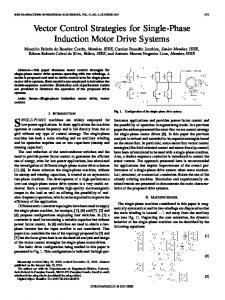
Fig. 7. Vector control Induction Motor Drive with neural network based space vector modulated VSI.
largest ni , ni+1 and their corresponding indexes (i.e. i and i+1) are selected by Kohonen’s Fig. 5. Modified Kohonen’s competitive layer based implementation of the space vector modulation technique for VSI.
4. PERFORMANCE
competitive network. The on duration ( Ti and Ti+1 ) of the two adjacent space vectors are computed. The space vector Vi and Vi+1 are selected according to the value of i and i+1. When adjacent vectors and on times are determined the procedure for defining the sequence for implementing the chosen combination is identical to that used in conventional space vector modulation as depicted in Fig. 6. The proposed scheme for vector control induction motor drive with neural network based space vector modulated VSI is shown in Fig. 7. (000)
VCn
(001)
(011)
(111)
(011)
(001)
(000)
1 0
VBn
1
0
VAn
1
0
t = kT s
S0
S1
T0
T1
S2 T3
S7
S2
T7
T3
"1" = V /2 ,"0" = -V /2 dc dc
S1 T1
S0 T0
t = (k + 1)T s
EVALUATION OF VECTOR CONTROLLED INDUCTION MOTOR DRIVE WITH NEURAL NETWORK BASED SPACE VECTOR PWM Modified Kohonen’s competitive layer based space vector PWM was integrated with the inverter for rotor flux oriented vector controlled induction motor drive. The inverter was operated at switching frequency of 10 kHz (i.e. Ts =0.1 ms). The parameters of the induction motor considered in this study are summarized in Appendix. The performance of vector control induction motor drive with neural network based space vector PWM is presented during starting, load perturbation and speed reversal. Fig. 8. shows time response of speed, current and duty cycle for no load condition for neural network based SVPWM and conventional SVPWM respectively. Fig. 9. shows time response of speed, current and duty cycle for load perturbation at 0.35 sec. to 0.55 sec. for neural network based SVPWM and conventional SVPWM respectively. Fig.10. shows time response of speed, current and duty cycle for speed reversal for neural network based SVPWM and conventional SVPWM respectively. Neural network based SVPWM vector control induction motor drive shows high level of performance during starting, speed reversal and load perturbation.
Fig. 6. Pulse patterns generated by space vector modulation in sector 1
581
Journal of Theoretical and Applied Information Technology © 2005 - 2008 JATIT. All rights reserved. www.jatit.org
(b) Conventional SVPWM induction motor drive.
(a) Neural Network based SVPWM induction motor drive.
(a) Neural Network based SVPWM induction motor drive.
(b) Conventional SVPWM induction motor drive.
Fig. 8. Time response of speed, currents and duty cycle for no-Load
Fig. 9. Time response of speed, currents and duty cycle for load perturbation at 0.35 sec. to 0.55 sec.
582
Journal of Theoretical and Applied Information Technology © 2005 - 2008 JATIT. All rights reserved. www.jatit.org
(a) Neural Network based SVPWM induction motor drive.
(b) Conventional SVPWM induction motor drive.
Fig. 9. Time response of speed, currents and duty cycle for speed reversal at constant load.
5.
CONCLUSION
Use of ANN based technique avoids the direct computation of non-linear function as in conventional space vector modulation implementation. The ANN based SVPWM can give higher switching frequency which is not possible by conventional DSP based SVPWM. Switching frequency can be easily extended up to 50 kHz with dedicated hardware ASIC chip. The results demonstrate the ability of the proposed scheme to improve the performance and robustness of the vector-control drives.
6.
APPENDIX
Nominal power Stator resistance
2.2KW 1.77 ohms
R r
Rotor resistance
1.34 ohms
X
Stator leakage reactance Rotor leakage reactance Mutual reactance
5.25 ohms
R s
X X
ls
lr m
0.025 Kg.m2 4
[1] Ned Mohan, Advanced electric drives analysis, control and modeling using Simulink. MNPERE Minneapolis, USA. [2] Peter Vas, Artificial- intelligence- based electrical machines and drives application of Fuzzy, Neural, Fuzzy-Neural and Genetic Algorithm based techniques. Oxford University press, London. [3] Keliang Zhou and Danwei Wang , “Relationship between space-vector modulation and three-phase carrier-based PWM: a comprehensive analysis”, IEEE Transaction on Industrial Electronics, Volume 49, Issue 1, Feb. 2002, pp.186 – 196. [4] Sun Jian and H. Grotstollen, “Optimized space vector modulation and regularsampled PWM: a reexamination” IEEE Industry Applications Conference, 1996, Volume 2, Oct. 1996 , pp. 956 – 963. [5] S.R. Bowes and Lai Yen-Shin, “The relationship between space-vector modulation and regular-sampled PWM” IEEE Transactions on Industrial
The parameters of induction motor are as follows: P
J Rotor inertia p Number of pole REFRENCES
4.57 ohms 139 ohms
583
Journal of Theoretical and Applied Information Technology © 2005 - 2008 JATIT. All rights reserved. www.jatit.org
Electronics, Volume 44, Issue 5, Oct. 1997, pp. 670 – 679. [6] Bai Hua, Zhao Zhengming, Meng Shuo, Liu Jianzheng and Sun Xiaoying, “Comparison of three PWM strategies-SPWM, SVPWM & one-cycle control” Fifth International Conference on Power Electronics and Drive Systems, 2003, Volume 2, Nov. 2003, pp. 1313 – 1316. [7] B.P. McGrath, D.G. Holmes and T. Meynard, “Reduced PWM harmonic distortion for multilevel inverters operating over a wide modulation range” IEEE Transactions on Power Electronics, Volume 21, Issue 4, July 2006, pp. 941 - 949. [8] C. Wang, B.K. Bose, V. Oleschuk and J.O.P Pinto, “Neural Network based space vector PWM of a three level inverter covering overmodulation region and performance evaluation on induction motor drive” in Proc. Conf. Rec. IEEE IECON, 2003, pp. 16. [9] A. Bakhshai, G. Joos, J. Espinoza and H. Jin, “Fast space vector modulation based on a neurocomputing digital signal processor” Applied Power Electronics Conference and Exposition, Conference Proceedings 1997, Volume 2, Feb. 1997, pp.872 - 878 . [10] A.R. Bakhshai, G. Joos, P.K. Jain and Jin Hua, “Incorporating the over modulation range in space vector pattern generators using a classification algorithm,” IEEE Transactions on Power Electronics, Volume 15, Issue 1, Jan. 2000, pp. 83 – 91.
584