1
A VLSI field-programmable mixedsignal array to perform neural signal processing and neural modelling in a prosthetic system Simeon A. Bamford1,3∗ , Roni Hogri2∗ , Andrea Giovannucci3 , Aryeh H. Taub2 , Ivan Herreros3 , Paul F.M.J. Verschure3,4 , Matti Mintz2 , Paolo Del Giudice1 1
Complex Systems Modelling Group, Istituto Superiore di Sanità, Rome,
[email protected]. 2
Psychobiology Research Unit, Dept. of Psychology, Tel Aviv University. 3
Laboratory for Synthetic, Perceptive, Emotive and Cognitive Systems, Universitat Pompeu Fabra, Barcelona. 4
Catalan Institute of Advanced Studies.
∗
Equal contributors - see Attributions and Acknowledgements for details. Abstract—A VLSI field-programmable mixed-signal array specialised for neural signal processing and neural modelling has been designed. This has been fabricated as a core on a chip prototype intended for use in an implantable closed-loop prosthetic system aimed at rehabilitation of the learning of a discrete motor response. The chosen experimental context is cerebellar classical conditioning of the eye-blink response. The programmable system is based on the intimate mixing of switched capacitor analogue techniques with low speed digital computation; power saving innovations within this framework are presented. The utility of the system is demonstrated by the implementation of a motor classical conditioning model applied to eye-blink conditioning in real time with associated neural signal processing. Paired conditioned and unconditioned stimuli were repeatedly presented to an anaesthetised rat and recordings were taken simultaneously from two precerebellar nuclei. These paired stimuli were detected in real time from this multi-channel data. This resulted in the acquisition of a trigger for a well-timed conditioned eye-blink response, and repetition of unpaired trials constructed from the same data led to the extinction of the conditioned response trigger, compatible with natural cerebellar learning in awake animals.
I. I NTRODUCTION Where brain functions are impaired through brain damage or through degeneration caused by ageing, it may be possible to develop prostheses which could interact with the brain in order to replace this functionality. While existing neural prostheses either provide input to the nervous system (e.g. cochlear prostheses [1], deep-brain stimulators [2] etc.) or take output from it (e.g. motor cortical prostheses [3]), a largely unmet challenge is the creation of devices that take input from the brain and provide output to it, in order to replace or supplement the functionality of a circuit internal to the brain, although software-based prototypes are appearing [4, 5]. The aim of the European ReNaChip project [6] was to provide a proof of concept for such a closed-loop prosthetic system. The cerebellum was chosen as a target brain area because its well-defined inputs and outputs facilitate physical interventions whilst its relatively simple internal structure have proved
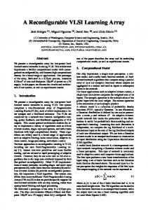
fertile grounds for neural modelling from Marr onwards [7]. Eye-blink conditioning was chosen as a well studied target behaviour against which success can be measured. It is intended that the replacement system should be biomimetic, i.e., its architecture and functionality should mimic the characteristics of the area which it replaces according to a neural model of the behaviour of the area. Whilst the system is not specifically intended for clinical application, there has been a focus on practical constraints such as miniaturisation and power constraints for implantability. The project has involved electrode design, neurophysiology, modelling of cerebellar learning, signal processing methods, real-time system integration and chip design. This article focuses on chip design, particularly how a field-programmable mixed-signal array is used to fulfil the computational requirements. Firstly, in sect. II, the target system is described, including: the eye-blink paradigm; electrode placements for recording and stimulation; signal processing methods for real-time extraction of stimulus related events from neural recordings; and the model of cerebellar function which allows on-line learning. Then in sect. III the chip prototype is introduced and its features explained. The key experiment by which the performance of the developed circuitry is demonstrated is the real-time acquisition and extinction of a learnt timed response based on in vivo recorded data, for which methods and results are presented in sect. IV and V, respectively. II. TARGET PROSTHETIC SYSTEM A. Eye-blink conditioning Eye-blink conditioning is a form of classical conditioning that is commonly investigated with the delay paradigm [8]. An auditory stimulus (conditioned stimulus - CS) and air-puff to the eye (unconditioned stimulus - US) are applied according to the timing scheme in fig. 1a (bottom), in which the CS onset precedes the US onset by an inter-stimulus interval (ISI) of a few hundred ms and the two stimuli then co-terminate. A US alone causes the subject, whether human or rodent, to blink; this is called an unconditioned response (UR). After many repetitions of these paired stimuli, however, the subject learns to blink in response to the CS, prior to the US, at an appropriate time to anticipate the aversive stimulus; this is called a conditioned response (CR). It is known that the cerebellum is necessary for this learning to occur [9]. The target structure for replacement, therefore, is a microcircuit of the cerebellum. The cerebellum has two inputs and one output, as shown in fig. 1c. Inputs related to all sensory stimuli come from the pontine nucleus (PN) while sensory inputs related to inherently aversive stimuli (US) also come from the inferior olive (IO). Both inputs arrive at the Purkinje cells (PU). Output from PU is inhibitory to the deep cerebellar nuclei (DN). A learnt timed response manifests itself as activation of specific DN cells, from where signals go to premotor nuclei including the red nucleus and on to motor nuclei, such as the facial nucleus (FN) from where, in the case of this paradigm, an eye-blink is elicited.
2
Amp Amp
Event detection
Cerebellar model
Event detection
300−3000Hz
Stimulator
PN Airpuff
IO
1
CS
PU
FN
White noise
2
PU PN
Rectified
DN
IO 3
CR 0.2−1.6Hz
Anaesthetised rat
US
FN
4
5
6
7
CS Thresholded
US 0.0
0.1
0.2 Time (s)
0.3
(a)
0.4
−0.5 0 0.5 Time relative to onset of CS (s)
1
(b)
Auditory stimulus Eye-blink (c)
Airpuff
W (d)
Figure 1: (a) System overview: electrodes in PN and IO bring signals to amplifiers; amplified signals are processed leading to detection of CS and US events, respectively (see b); the detected events are inputs to a model of cerebellar learning (see d); the output triggers a stimulator to elicit an eye-blink response via an electrode in FN; in a “paired” trial for CR acquisition, a white noise stimulus (CS) and an air-puff (US) occur in the sequence shown at the bottom, i.e. US starts 0.3 s after CS, and they co-terminate after another 0.1 s; (b) Event detection example for multi-channel data from PN encompassing a CS event: the period of the CS is shown as vertical lines at 0 s and 0.47 s; incoming data from the PN electrode is amplified, band-pass filtered (300-3000 Hz) and the 3 channels are summed together to yield the top trace; this is rectified (second trace), and then band-pass filtered (0.2-1.6 Hz) to yield the third trace; hysteretic thresholds, shown as two horizontal lines, are then applied to yield the detected digital event in the bottom trace; the delay of onset detection of ≈ 100 ms is partly explained by neural transduction through the auditory pathway and mainly by the time taken to aggregate information before making a decision; the hysteretic threshold captures the duration of the CS event (after the onset delay) without detecting false alarms from the smaller threshold incursions; magnitudes on y-axis are arbitrary. (c): Simplified cerebellar microcircuit. (d) Cerebellar learning model: CS onset (1) triggers slow reduction of PU activation; when this goes below a threshold (2) it triggers CR, and after a fixed delay (3) IO is inhibited; synaptic weight (W) rises during CS due to LTP; the US events shown here do not refer to the protocol in (a) but rather indicate how the learning model responds to paired stimuli with various timings; a US event prior to CS (4) does not trigger LTD but during CS (5) does cause a fixed amount of LTD (reduction of W); after CR is produced, US events still trigger LTD (6) until the IO inhibition (3) after which they do not (7); during CS, therefore, W reduces in response to US occurring before and slightly after CR, and otherwise increases.
The intended overall system is shown schematically in fig. 1a. Recording electrodes are inserted in PN, where a neural response to the CS can be detected, and in IO, where a response to the US can be detected. The signals from the recording electrodes are amplified and go through various stages of filtration (as detailed in the figure caption and sect. IV-B), resulting in detections of CS and US events. These are input to a model of cerebellar function, whose output may be a timed response to a CS event. This output (the modelled CR) triggers a stimulator which elicits an eye-blink (behavioural CR) through an electrode implanted in FN. The system is therefore meant to bypass and emulate the neural circuitry that implements learning and effects the appropriately timed response. The following sections provide more detail on the aforementioned parts of this system. B. Event detection The signals from the electrodes are treated as multi-unit; i.e., the aim is to detect energy related to a population of spikes rather than to identify spikes from particular neurons; an increase in energy is observed in response to the stimuli, which is typically sustained in the case of PN [10] and phasic in the case of IO. The signal is amplified (gain ≈10000×) and
filtered in the frequency band associated with spikes (typically 300-3000 Hz), resulting in traces of magnitude ≈0.1V RMS. For the multi-channel electrode in the PN, the signals are summed together according to a weighting calculated offline, based on the quality of event detection that can be obtained from each channel separately. Then signals are rectified and band-pass filtered to yield a measure monotonically related to the energy over a small window of time (the energy envelope), and a threshold is applied to yield onsets and offsets of detected events. The high cut-off frequency of the band-pass filter is a compromise between the need to detect events immediately to act on them in real-time, and the need to aggregate more information over a longer period to make better detections. The low cut-off frequency is not critical but removes long-term drifts in the background energy in traces, as can be observed in acute experiments with anaesthetised animals. For PN, where detections may last a few hundred ms, the band is on the order of 0.1-1 Hz (CS detection should at least occur prior to the minimum ISI that can be learnt, which might be≈150 ms [11]), whereas for IO, where the phasic response may be as short as 25 ms, the band is ≈1-10 Hz. The thresholding of the PN trace is hysteretic, so that given the typical pattern of response with a large phasic component followed by a smaller sustained component, the offset time
3
can be detected without lowering the threshold, which would increase false positive detections. Fig. 1b shows an example of this procedure (which is common for a range of biosignals [12, 13]). C. Cerebellar model The learning model of the system presented here is based on a biologically constrained model of the cerebellum and its role in classical conditioning [14, 15, 16]. Fig. 1d presents a simplified scheme. The time course of the CR depends on the total effective excitatory drive onto the PU cells that is adjusted through the interplay of long-term potentiation (LTP) caused by the CS and long-term depression (LTD) caused by the US in the presence of the CS. Learning through LTD causes the CS derived input to a specific PU to diminish. As a result this PU will start to pause in its response to a CS. Due to the absence of PU activity the DN is released from inhibition and a CR is triggered. LTD caused by coincident CS and US events incrementally reduces the input to the PU and brings forward in time the moment at which a CR is triggered. Over many pairings, the timing of the eye-blink will precede that of the US and will be considered a CR. The correct timing of the response is stabilised through a negative feedback from DN to IO which, once activated to deliver a CR, also blocks US signals from being conveyed to the cerebellum, thus preventing further LTD. The feedback delay of this loop is tens of ms [17], which serves to match peripheral delays in the production of an eye-blink. In the continued absence of paired trials, LTP caused by the CS alone will ultimately extinguish a previously learnt timed response. The real-time features of this model have been previously assessed using robotic experiments and key features of this model have already been implemented in an aVLSI form [16]. Further validation has been obtained by interfacing it directly to the brain [4]. The model is interpreted in this work as high-level, not concerned with details at the level of spiking transmission or molecular mechanisms of plasticity, and not necessarily indicative of the behaviour of individual PU cells but rather as an aggregate behaviour. Nevertheless the model contains some elements common to neuromorphic electronic design, such as decaying time courses (as in the activation of PU cells during the CS), events triggered by threshold crossings (as in the CR event caused by the reduction of PU to DN inhibition below a certain level), the need for the storage of a value representing (in this case aggregate) synaptic weight and integration of plasticity events on that value, based on relative timing of events (as in the application of LTP based on a CS event and the application of LTD based on the arrival of a US event during a CS event). III. C HIP DESIGN A. Prototype chip A chip prototype has been designed and fabricated to implement the cerebellar microcircuit replacement prosthesis described in sect. II. The design respects many of the constraints
of implantation, although the current prototype does not offer a standalone solution. The chip (fig. 2a) contains three cores, (1) a voltage bias generator; (2) low noise neural amplifiers; (3) a field-programmable mixed-signal array (FPMA). The FPMA core is capable of implementing event detection (sect. II-B) and the cerebellar model (sect. II-C) and is the focus of this article. Other cores are not used in this work; any voltage biases necessary are supplied externally, and the amplifier core (which would include the first stage of filtration in fig. 1b) is by-passed, with pre-amplified and pre-filtered signals brought to the inputs of the programmable array. Note that a complete solution would also contain a core for generating stimulation pulses, whereas this prototype can be used to trigger an external stimulator. This section introduces and describes the programmable core. A typical field-programmable gate array (FPGA) contains an array of digital logic primitives which are surrounded by a matrix of programmable interconnect such that primitives can be wired together by setting digital switches; thus arbitrary digital computers can be constructed. Such devices are commonly used especially in prototyping systems. The fieldprogrammable analogue array (FPAA) concept is similar except with analogue computational primitives. Various authors have attempted to use diverse primitives in FPAAs, including transistors [18] current-mode circuits [19], switched capacitors (SC) [20], and higher level compound blocks [21, 22]. The many different possible requirements of analogue circuits suggest a spectrum of different design choices from the choice of primitives upwards and dictate against the generality achievable with FPGAs, limiting application of a given FPAA architecture to a given application domain. It will be argued in sect. VI-B that, with certain design choices, neural signal processing and neural modelling is a promising domain for this technology. The core that has been created is a field-programmable mixedsignal array (FPMA), but not in the usual sense of an FPGA and an FPAA core on the same chip with a layer of analogue-to-digital and digital-to-analogue converters (ADCs and DACs) separating their domains [23, p. 71] [24]. Rather digital and analogue signals are mixed “intimately”, sharing the same routing resources, and a key novelty is the method of controlling currents to allow this mixing (sect. III-E). The general approach taken is to work with discrete-time voltage-mode signals by means of SC circuits; this is a common choice for academic and commercial designs alike [20, 25, 26, 27]. The SC technique emulates resistances by switching the terminals of capacitors; this standard technique will not be explained here. The primitives (hereafter “components”) are of 4 types: pulse generator (PGN), configurable switched capacitor (CSC), operational transconductance amplifier (AMP) and configurable logic block (CLB); schematics are shown in fig. 2b. They are laid out in an island-style topology [28], with relatively permissive routing which is not optimised for low path impedance. Configuration of components and routing is by the rowparallel programming of SRAM cells distributed throughout the chip. There are 500 components of the various types;
4
this is therefore a fine-grained design, (whereas most commercial designs have offered a small number of components [27, 26, 29]), and the intention is to operate with many small, low-quality components, using a combination of calibration and pooling of components to deliver accuracy where it is required. For details of the core architecture see fig 2c.
(a) The chip uses a 0.35 µm process (Austria Microsystems), and has dimensions 4.8×3.8 mm. Cores are indicated on the photo. Pulse Generator (PGN):
Amplifier (AMP):
Enable In+ In-
B. Switched capacitor optimisation
Out
Configurable Logic Block (CLB): In1 (H) In2 (H) In3 (L)
Out
Look-up table D
Clk
Flip-flop
MUX
Limitation of power consumption is a major concern for implantable hardware and a prominent reason for working with analogue circuitry. In the following 4 sections, key aspects of this design are described that limit power consumption and otherwise make it fit for the domain of neural signal processing and neural modelling. These aspects are: switched capacitor optimisation (sect. III-B); current control (sect. III-C); leakage limitation (sect. III-D); and the mixing of analogue and digital signals (sect. III-E). Then sect. III-F, shows how rectification is performed, as an example computation which utilises all components and which is part of the signal processing chain of sect. II-B.
Out
Configurable Switch Capacitor (CSC):
The choice of SC circuitry allows great flexibility but is not ideal for power consumption, since repetitive charging and discharging of clock nodes can pass significant current with respect to the charging and discharging of the voltage-mode signal nodes that they act on. Nevertheless there is much that can be done to limit power consumption. Firstly, CSCs are clocked by a single signal and each contain a state machine for locally generating a pair of non-overlapping pulses in response to a rising edge (fig. 2b). This halves the power used in charging and discharging clock nodes compared to transmitting the two non-overlapping clocks on separate wires. Secondly, clocks are not global but rather generated by PGNs and routed only to where they are needed. The CSCs take their clock signals from the programmable matrix, also allowing them to pass single packets of charge in response to irregular events generated elsewhere within the array; this has possible uses in neuromorphic modelling, a novelty which sets this design apart from other SC FPAAs, but which is not exploited in this article. The aforementioned state machine is insensitive to the slew rate of the clock, thus reducing the requirement for the strength of the driver of the clock signal, which needs to source and sink current only just fast enough to charge and discharge the clock node once per cycle. (The state machine is based on the slew-rate insensitive D-type flip-flop of [30]). This can reduce the effect of clock noise in the system, since clock nodes typically slew much more slowly than in digital systems, meaning that driven nodes onto which these signals are coupled may have much smaller transients as a result. Thirdly, PGNs can be enabled by routed digital signals, thus processes that are active with only a short duty cycle (there are many within the cerebellar model, see sect. IV-D) may consume much less power than if they were continuously clocked.
Polarity State machine: Rising edge to non overlapping pulses
Cap array
Switch config
Clk
(b) Simplified schematics of the 4 components types. The CLB (sect. III-E) is as in [30] with an additional high-starved input (“H”). The CSC (sect. III-B) has 2 switched inputs to each side of its capacitor and can work in lossless as well lossy modes [31], or as an analogue switch or a static capacitor; the capacitance is an array programmable by SRAM [as in 20, fig. 6], in the range ≈50 fF - 1.6 pF. “Polarity” explained in sect. III-F. For PGN see sect. III-B; For AMP see sect. III-D. Wire segment PGN
AMP
CSC
CLB
AMP
CSC
CLB
Switch block
PGN
Connection block
(c) Components are laid out in an island-style topology [28]. Each routing bus has 8 wires (only 4 are shown for clarity), wire segments span one row or column of the component array and the switch blocks connect each wire terminal to 5 others (relatively permissive [28, sect. 5.1.3]). Switches (shown as dots) are transmission gates (T-gates; i.e. an NMOS and a PMOS in parallel) each gated by a dedicated SRAM cell. Configuration of components and routing is by row-parallel programming of SRAM distributed throughout the chip; the chip is laced with 337 word lines and 410 bit-line pairs driven by standard programming circuitry in the periphery; these define a grid of possible SRAM locations of which ≈60,000 are occupied. Each 8-transistor SRAM/T-gate cell uses ≈ 54µm2 . The core has dimensions 1.6×2.9 mm; this area is dedicated to: routing switches 58%; components - 34%; and bias generators (sect. III-B) and decoupling capacitors - 8%. There are 500 components: 40 PGNs, 120 CSCs, 180 AMPs and 160 CLBs.
Figure 2: Chip design overview
5
C. Current control The signals involved in the initial stages of the chain of filters must pass signals of up to 3 kHz, implying a Nyquist rate of 6 kHz and a clock frequency for CSCs significantly higher (the core has been designed for frequencies up to ≈ 100 kHz). Later stages in the process have high cut-off frequencies on the order of just 1 Hz, and the cerebellar model of sect. II-C needs a slowly ramping signal representing PU activation (trace 2 of fig. 1d) which decreases over a period of order 1 s, for which clocked processes of order 10-100 Hz may be sufficient. There is therefore a range of greater than 3 orders of magnitude of different frequencies of operation and it should be possible to set the currents associated with these various processes appropriately so as not to waste power. The core is divided into 10 bands of components, each of which has associated bias currents which can be set to bias the AMPs, the CSCs’ state machines, and the CLBs (sect. III-E). It is intended that different circuitry operating at different speeds be placed within these bands, so that only those components with a high speed requirement are run at high power. The 24-bit programmable current generators of [32] have been reworked for SRAM programming. The currents are used both to bias components and to drive oscillators in the PGNs. The current of each generator can be individually altered over several orders of magnitude from a master current of 2 µA down to < 1 pA, producing oscillator frequencies from ≈ 100 kHz down to