sors by spraying a mixture of nonconductive polymers and carbon black particles ... [1, 2] employing carbon black and non-conducting polymers. Exposure to ...
AN INTEGRATED CHEMICAL SENSOR ARRAY USING CARBON BLACK POLYMERS AND A STANDARD CMOS PROCESS Jeffrey A. Dickson1, Michael S. Freund2, Nathan S. Lewis2, Rodney M. Goodman1 1
Department of Electrical Engineering 2 Department of Chemistry California Institute of Technology Pasadena, California 91125
even wearable chemical sensor arrays that rival the detection and discrimination capabilities of mammalian olfaction.
ABSTRACT We have developed a new chemical sensor array by combining polymer-based chemiresistors with a standard integrated circuit technology. We fabricated an array of addressable chemical sensor sites in a CMOS process, and then performed a post-processing step of electroless gold to create sensor contacts. We create sensors by spraying a mixture of nonconductive polymers and carbon black particles onto the sensor sites. We demonstrate that an array of diverse chemical sensors can perform discrimination of odors.
DESIGN AND FABRICATION The sensor consists of an array of individually addressable electrical contacts, on which a polymer/carbon black mixture is deposited. The sensor technology is well suited to integration with on-chip circuitry. The array allows each sensor to be individually addressed. Figure 1 shows the schematic of the unit sensor cell. The cell consists of a switch transistor and decoding logic. The availability of only two metals layers in the IC process required transistors at each sensor cell to perform decoding. This circuitry (M1-M4) decodes X and Y selection signals generated by shift registers on the periphery of the array. This selection signal controls a switch (M7) that toggles a current (Iin) through the resistive sensor. In this design only one sensor is energized at a time to reduce power consumption. To reduce noise and the switch resistance, transistor M7 occupies most of the sensor area. The decoding circuitry also selects a transmission gate (M5,M6,M8,M9) which passes the sensor voltage to a column output bus. This signal is amplified and transmitted off-chip for processing. The decoding circuitry is complicated because the sensor occupies one of two available metal layers in the fabrication process we used for this chip, precluding the use of a simplified bus scheme.
INTRODUCTION This paper describes the development of an array of chemical sensors. The sensors are based on the polymer approach of Lewis et al.[1, 2] employing carbon black and non-conducting polymers. Exposure to particular analytes causes the sensors to swell, which increases the electrical resistance. By employing different polymers we can create a large number of different broadly tuned sensors. Since they can be fabricated at room temperature and a change in resistance is easily measured, this technology is attractive for integration with active circuitry. This array is capable of chemical discrimination that does not require external excitation or complicated signal processing like optical sensing[3]. Unlike SAW devices, we can integrate large arrays on the same chip[4]. Applications including environmental monitoring, narcotic and explosives detection have demanding chemical sensing requirements. Our goal is to create small, inexpensive, low power and Iin M1
M2
M7
COL
M5 M8
Vout M3 M9 SENSOR
M4
M6
ROW
Figure 1 Schematic of three wire sensing cell. Transistors M1-M4 form a NAND gate to select the cell, M7 switches the current source on sensor resistor, and M5,M6,M8,M9 form a transmission gate to select the output on a column output line. The column output is buffered and passed off-chip.
Figure 2 Photograph of the integrated sensor chip, after post fabrication electroless gold plating and polymer deposition by airbrush. The chip contains 492 sensor sites arranged in a 41X12 array. On this test chip 209 sensor sites have been covered with one of eight different polymer based chemiresistors. Shift registers located along the left and bottom of the array select an individual sensor site, whose output is amplified and passed off chip. The chip is 0.5 cm by 0.25 cm. Figure 2 shows the 0.5 cm X 0.25 cm chip, with 492 sensors arranged as an array of 41 X 12 sites, fabricated in a 2.0 micron process through the MOSIS design service. The dark vertical bars on the chip are deposited chemical sensors, discussed later in the text. A close-up of the individual sensor sites its shown in Figure 3. There are two contacts to the sensor: one with the drive switch M7, and another connecting the sensor to signal ground. The ground terminal is laid out as a ring around the perimeter of the cell and is common to all sensors. The interior of each cell contains the drive contact for the sensor. The ring structure was motivated by difficulties encountered in early sensor deposition trials – the carbon black particles would aggregate along the perimeter of a deposited sensor, creating a low resistance path. Moreover, the ring structure allows us to experiment with depositing mixtures of sensor materials across the chip[5]. We deposit the sensor polymer between these two contacts, directly on top of the active circuitry. We make the sensors rectangular to increase the contact area for the interior contact, as well as to reduce contact noise and 1/f noise due to the non-uniform electrical field[6]. We use a standard commercial foundry for the fabrication of the integrated circuits. The top layer of Aluminum is used for the sensor contact. Unfortunately, the native aluminum oxide that forms on the contacts prevents depositing the sensors without a post-processing step. Since dedicated wafer runs are cost prohibitive for small prototyping runs, this step must be performed on the individual chip die returned from the foundry. This precludes the use of a conventional mask based approach, since it is difficult to use a resist mask on an individual die. To create suitable contacts we use an electroless Ni/Au process that requires no masking from Stapleton Technologies (Long Beach, California). This process can be performed easily on individual die with simple equipment and requires only seven procedures: four involving cleaning and surface preparation and
three plating steps. The surface preparation involves an acid zincate process to remove the native oxide and activate the aluminum surface. This is followed by the three plating steps. Nickel is plated first, followed by a two stages of gold plating: a monolayer process that plates the Nickel and then a build up stage that finishes the plating. Figure 3 shows three sensors, plated with 9 microns of Ni and 1 micron of Au. In addition to creating a nonreactive surface for the sensor contacts, the plating also creates wells that help constrain the sensor material during deposition.
Figure 3 Picture of three sensor sites after the electroless gold plating. The central bars are the switched output node of each individual sensor. The surrounding conductor is a common ground. The sensor material is deposited on top of the chip, forming the sensor between the central contact and the surrounding ground The sensors are a combination of a particular polymer and carbon black particles. To prepare the sensor material we combine 20 mg of Carbon Black and 80 mg of the polymer in powder form. The polymers and solvents are shown in Table 1. The Carbon Black we used is a furnace black from Cabot Co. (Billerica, MA). We place the mixture in an ultrasonic bath for a minimum of five min-
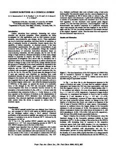
5
utes to suspend the carbon black particles before depositing the sensors. Solvent Toluene Toluene Toluene THF Acetone THF Ethanol THF
Voltage (V)
4
Polymer PEO PEVA p-Butadiene p-vinyl carbazole p-vinyl acetate p-capraclactone p-vinyl pyrrolidone p-4-vinyl phenol
3
R = 530 kOhm
2
1
0 0
4
6
8
10
Input Current (10E-6A)
Table 1 Listing of the eight polymers and the corresponding solvents used in the fabrication of the chemiresistors. To deposit the sensor material on the surface of the integrated circuit we employed an airbrush. A sheet of polyamide 50 microns thick is used as a physical mask to define the sensors. Apertures are cut in the polyamide using a computer-controlled laser. While other materials and processes are available to make this mask, the polyamide gaskets well to the surface of the chip. In addition, the ability to see through the polyamide allows us to position the mask accurately. We are able to create apertures as small as 50 microns using this technique, enabling us to spray individual sensor sites. We sprayed eight different polymers (Table 1) in columns two sensors (270 ? m) wide. Figure 4 shows a close-up of the sprayed chip, demonstrating the ability to fabricate small sensors on the chip. The spraying of the polymer allows us to create thin, uniform films of sensor material. Previously we used a direct deposition technique using a fine tip that resulted in uneven deposition and thick films.
2
Figure 5 Voltage vs. Current sweep of an individual sensor node, demonstrating its linear resistive nature. At