IEEE TRANSACTIONS ON CIRCUITS AND SYSTEMS—I: REGULAR PAPERS, VOL. 60, NO. 1, JANUARY 2013
11
An Order-Statistics Based Matching Strategy for Circuit Components in Data Converters Tao Zeng, Student Member, IEEE, and Degang Chen, Senior Member, IEEE
Abstract—Random mismatch errors in matching-critical circuit components cause variability in component parameters, which in turn degrade linearity performance and parametric yield of data converters realized by these components. Utilizing results from the area of order statistics, this paper introduces a novel random mismatch compensation theory called ordered element matching. By pairing a small parameter component with a large one, it effectively reduces the standard deviation of the mismatch errors by a factor of at least 6.5 in a reasonably sized component population. An order-statistics based outlier elimination strategy further improves the standard deviation and more importantly reduces the differential nonlinearity by a factor of 2 or more. Building on these, a new technique called complete-folding is developed, which selectively converts a unary-weighted array to a binary-weighted array and consequently reduces the differential nonlinearity and integral nonlinearity by another factor of more than 3 and 8, respectively. Monte Carlo simulations are performed in a high-resolution data converter design to quantitatively compare the matching performance achieved by complete-folding technique with state of the art. Significant improvements on linearity performance and design cost are obtained. Index Terms—Data converters, linearity, order statistics, random mismatch, yield.
I. INTRODUCTION
D
ATA converters are the interfaces for information flowing between the digital and real worlds. They play crucial roles in many electronic circuits and systems today. Analog-todigital converters (ADCs) covert an analog voltage or current into digital domain for further digital signal processing, whereas digital-to-analog converters (DACs) convert digital information into analog domain as representations of voltage, current, or electric charge to carry out real-world functions. Many ADCs [1]–[10] and DACs [11]–[20] rely on matched circuit components such as transistors, resistors, or capacitors to perform their data conversion tasks. However, the integrated-circuit (IC) fabrication technology invariably produces imperfectly matched circuit components. The imperfections lead to component parameters deviating from their designed values. The resulting errors contain a significant random part which is determined by the inherent matching properties of the fabrication process, and they are often termed as random mismatch. As IC technology continues to advance, motivated by Moore’s law, random mismatch becomes significantly worse due to shrink of device size Manuscript received February 17, 2012; revised April 09, 2012; accepted May 08, 2012. Date of current version January 04, 2013. This work was supported in part by Texas Instruments Inc. and the National Science Foundation. This paper was recommended by Associate Editor J. Li. The authors are with Department of Electrical and Computer Engineering, Iowa State University, Ames, IA 50011 USA (e-mail:
[email protected];
[email protected]). Digital Object Identifier 10.1109/TCSI.2012.2232991
and supply voltage [21]–[23]. Since it causes electrical property variations of the fabricated elements which result variability in circuit properties, random mismatch is considered as one of the major sources of error that degrades linearity performance and parametric yield of many analog and mixed-signal circuits and systems, especially of data converters. The variations in component parameters caused by random mismatch are random in nature, and thus they are modeled as random variables with mean of zero and standard deviation related to the physical area of matching-critical components [24]–[29]. In general, a factor of four augmentation in area corresponds to a factor of two reduction in standard deviation of the mismatch errors. Therefore, 1-bit linearity enhancement will lead to a quadruple of circuit area. Nevertheless, the maximum allowed area is limited by the available die size as growing number of circuits and systems are integrated into a single chip. Additionally, large device dimensions deteriorate parasitic capacitance effects which limit the achievable speed of data converters and in some cases increase the power consumptions [10], [30]. Besides increasing the area, many other techniques can be applied to compensate random mismatch errors in the matching-critical components for data converters. They can be divided into four categories, i.e., trimming, calibration, switching-sequence adjustment, and dynamic element matching (DEM). Each category is briefly discussed in the following paragraphs. Trimming compensates the random mismatch errors by regulating the component parameters at the wafer stage. It requires accurate test equipments to continuously measure and compare trimmed parameters with their nominal values. There are mainly two types of trimming. One is to change the physical dimensions of the circuit elements by applying laser beams [11], [19], whereas the other one is to connect/disconnect an array of binary-weighted small elements using fuses or MOS switches [29]. Both forms of trimming can be cost-ineffective in test time and equipments, and the achieved accuracy does not account for temperature and aging effects [31]. Calibration alleviates the random mismatch effect by feeding back either digital or analog correction signals to the data converters’ input or output after measuring errors based on an available reference. Calibration can be treated as an improved version of trimming since it characterizes errors on chip or board and continuously corrects them over different time and environments. Some calibration techniques have to be performed at circuit power-up or stand-by phase [11], [16], [17], while some can be done in background without any interference to the normal operation [5]–[7], [9], [10]. Yet, the obtained accuracy level is
1549-8328/$31.00 © 2012 IEEE
12
IEEE TRANSACTIONS ON CIRCUITS AND SYSTEMS—I: REGULAR PAPERS, VOL. 60, NO. 1, JANUARY 2013
limited by the resolution and accuracy of error measurement circuits and correction signals. Switching-sequence adjustment is commonly used in layout designs to compensate the systematic gradient errors [13], [14], [29]. In recent publications [18], [20], this method has been extended to compensate random mismatch errors in the data converters. It improves linearity performance by changing component switching sequence according to the parameter orders. That is to place an element having smaller parameter in neighbor with the one having larger parameter. However, this approach only improves the integral nonlinearity (INL), and the differential nonlinearity (DNL) remains unchanged which greatly limits the matching efficiency. DEM is another popular solution to the random mismatch errors for matching-critical components. It dynamically changes the positions of mismatched elements at different time so that the equivalent component at each position is nearly matched on a time average. Some examples of this technique can be found in [2], [3], [15], [32]–[34]. Among all of these, the popular algorithms are butterfly randomization [32], individual level averaging [33], and data weighted averaging [15], [34]. Unlike the static random mismatch compensation techniques, DEM translates mismatch errors into noise. However, the translated noise is only partially shaped where the in-band residuals could possibly affect the data converters’ signal-to-noise ratio (SNR) [35]. Furthermore, the output will be inaccurate at one time instant since DEM only guarantees matching on average, and thereby it cannot be implemented in some applications. In this paper, we introduce a novel random mismatch compensation theory called ordered element matching (OEM), which does not fall into any of the four categories mentioned above. It sorts the circuit components based on their parameter magnitudes, and then pairs and sums the complimentary ordered components. By doing so, it creates a new sample population with twice larger in magnitude but much smaller variations than those of the original sample population. Since random mismatch errors are modeled as random variables with certain statistical characteristics, a statistical analysis is performed to validate this theory. The statistics of the sorted and summed random variables can be obtained based on the theory of order statistics. The variation reduction factors are calculated by comparing the standard deviations of statistics between original and summed random variables. The OEM theory is derived based on the definition of quasimidranges in the subject of order statistics, where they are the half of the sum of complimentary ordered samples in a population [36]. Quasi-midranges sometimes serve as a fast estimation for the mean of a sample population; however, they are known to be sensitive to the outliers of parent distributions [36], [37]. This knowledge also holds for the OEM theory, and the standard deviations of those outlying summed random variables are shown to be substantially larger than the others in statistical analysis. Then, an outlier elimination strategy is proposed to omit a certain number of outlying elements in the original samples and thereby further reduces the parameter variations. More importantly, it considerably improves the DNL performance in a reasonably sized component population.
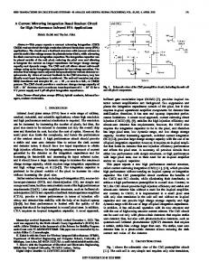
Based upon these, we develop a new matching technique called complete-folding, which can dramatically reduce both DNL and INL by selectively regrouping circuit elements according to their parameter orders and eventually transforming a unary-weighted array into a binary-weighted array. It has been demonstrated in [38] that this technique has a significant impact on linearity performance and parametric yield in a current-steering DAC design. In this work, statistical simulations are performed by using the complete-folding technique to justify the results obtained from the statistical analysis. This paper is organized as follows. Section II introduces the OEM theory in details along with statistical formulations using the theory of order statistics. Section III addresses the outlier elimination strategy and the ensuing standard deviation reduction based on statistical analysis. In Section IV, the basic functionality of complete-folding technique is illustrated, and meanwhile the circuit realization is briefly discussed. Section V presents the matching accuracy improvement in a current source array when both complete-folding and outlier elimination are applied. Comparisons are also made among the competing static random mismatch compensation techniques. Significant linearity enhancement and design cost reduction are observed. Finally, the paper is summarized in Section VI. II. ORDERED ELEMENT MATCHING Random mismatch errors in the matching-critical circuit components can severely degrade linearity performance and parametric yield of many data converters, because they cause random variations in the component parameters that lead to unpredictable circuit performance. The OEM theory is aiming at creating a new component population with significantly reduced variations according to the original component parameter orders. To facilitate the understanding of this new theory, Fig. 1 illustrates the matching process for a unary-weighted resistor array with sample size of 8. The rectangles in the figure denotes for the resistance values with random variations. The first step is to sort these resistors by their resistance values in the ascending order. All resistors are numbered from 1, 2 8 with their respective resistance. The second step is to pair the complimentary ordered resistors into one group. A series of paired resistors are organized as (1, 8), (2, 7), (3, 6), and (4, 5). The final step is to sum the two resistors within each pair and generate a new array of resistors with sample size of 4. The new resistors have resistance values that are twice as large as those in the original array, but their resistance variations are reduced considerably. This theory is also applicable to improve matching performance in the array of transistors or capacitors where the same procedure can be followed. In those cases, the rectangles in the figure would denote for drain currents and capacitance values, respectively. A. Statistical Formulation In order to quantify the amount of variation reduction by OEM, a statistical analysis is performed. Here, the random variations in the component parameters are modeled by a set
ZENG AND CHEN: AN ORDER-STATISTICS BASED MATCHING STRATEGY FOR CIRCUIT COMPONENTS IN DATA CONVERTERS
13
can be treated as normalized mismatch errors from the nominal value , and their statistical characteristics can be described by the probability density function (PDF) and cumulative distribution function (CDF), i.e., and , where (3) (4)
Fig. 1. The OEM procedure for a unary-weighted resistor array with sample size of 8.
of Gaussian distributed random variables. Gaussian distribution is used because: a) most engineers are more familiar with Gaussian distribution; b) Gaussian distribution is a good approximation for any random variables affected by a large number of intrinsic random variations, due to the central limit theorem; c) any other distributions can be approximated by Gaussian distribution if the mean is several standard deviations away from the distribution boundaries [39]. However, it should be pointed out that the following statistical analysis can be applied to any distributions, which indicates the OEM theory is even capable of compensating non-Gaussian mismatch errors. Considering the general cases, we take sample size of the original unary-weighted component array as 2n, where n is an integer number greater than 0. We will prove later that the variation reduction varies from population size selections. It should be also noticed random mismatch is the only considered source of error in this work. All other nonidealities in the matching-critical components such as gradient errors are assumed to be managed by the existing layout strategies [29]. Then, the parameter magnitude for each original circuit component can be expressed as: (1) where is the nominal parameter value, and and are the real parameter value and random mismatch error for the ith component, respectively. Random variables are assumed to be statistically independent and identically distributed (i.i.d.), and they follow Gaussian distribution with mean of 0 and standard deviation of , i.e., . On the other hand, random variables are also i.i.d. and follow Gaussian distribution with mean of and standard deviation of , i.e., . Our objective is to show the random variations can be significantly reduced by applying the OEM theory. To simplify the latter analysis, random variables are transformed into the standard Gaussian distribution according to: (2)
In the following analysis, we apply the OEM procedure to random variables , where they are sorted, paired and summed. The sorting step creates a series of ordered random variables, and the pairing and summing steps generate new random variables with sample size of n based on those ordered ones. The variation reduction factors are obtained by comparing the standard deviations between the original and summed random variables. B. Statistics of Ordered Components The first step of OEM is to rank the circuit components in the ascending order according to their parameter values. This is equivalent as sorting the random variables . Suppose are sorted in order of magnitude, and they are written as , then is called the ith order statistic [36]. To study the statistical characteristics of these ordered random variables , their PDFs and CDFs can be derived based on the theory of order statistics [40]:
(5) (6) and have the forms of (3) and (4), respecwhere tively. It is noted that the distribution functions for the ordered random variables are different from each other. For the ith order statistic , the expected value and variance can be obtained by computing the corresponding moments as formulated in [40]: (7) (8) (9) where r is an integer number greater than 0. It should be noticed the ordered random variables are no longer i.i.d. Instead, they become correlated after the sorting process. The covariance of the ith and jth order statistics ( and ) is denoted as , where
(10)
14
IEEE TRANSACTIONS ON CIRCUITS AND SYSTEMS—I: REGULAR PAPERS, VOL. 60, NO. 1, JANUARY 2013
Since the original population follows standard Gaussian distribution, we can derive two moment identities from (7), (8), and (9). They are given below:
Followed by this, the joint PDF of and can be derived by substituting in (14) with (15) as shown below:
(11) (12) The details of derivations can be found in [36] and [40]. Equation (11) indicates the expected values of the complementary order statistics ( and ) have the same magnitude but with opposite signs. Equivalently, they are symmetric at the mean value of original population, i.e., 0. On the other hand, according to (12), the variance should be the same for the complementary order statistics. Both equations will be used for the statistical analysis later when performing the pairing and summing steps.
(16) The marginal PDF of over :
is obtained by integrating out (16)
C. Statistics of Sum of Complementary Ordered Components The next steps of OEM are to pair and sum the complementary ordered components and generate a new population with sample size of n. This process can be viewed as the error compensation phase and it is as equivalent as adding the complementary order statistics from population in our analysis. The obtained new sample population is represented as , where (13) corresponds to the sum of the kth complementary order statistics. For example, represents the sum of minimum and maximum ( and ) in the original sample population. In addition, the sample size of the new population is reduced to n because of the pairing step. Intuitively, if we are adding the smaller and larger ordered values in a sample population, the sum tends to be twice as large as the population’s mean value. In our analysis, the sum will approach to 0, because the mean is normalized to 0. To provide the theoretical justification, we have to examine the statistical characteristics of the new random variables by obtaining their PDFs and CDFs. The first step is to find the joint PDF of the complementary order statistics, which can be derived from the joint PDF of two order statistics given in [36]:
(17) The CDF of
can be computed as: (18)
will have different distriFrom the derivations above, bution functions if k and 2n are assigned for different values. Consequently, the standard deviations of these new random variables will also be different. Then, when applying the OEM theory, the efficiency of the variation reduction will vary, depending on the order ranks and the original sample population size. The impact of these factors will be thoroughly addressed in the next subsection. The expected value and variance of are calculated by their corresponding moments as follows: (19) (20) (21) A direct way to obtain and is to combine (10), (11), (12), (13), (20), and (21) as illustrated below:
(22)
(23) (14) and where From (13), we have:
are given by (3) and (4), respectively. (15)
have expected Not surprisingly, all random variables value of 0. This is a very important observation, because it indicates the mismatch errors in the normalized sample population Z will be cancelled out by OEM. The same effect will also happen for mismatch errors in the original sample population
15
ZENG AND CHEN: AN ORDER-STATISTICS BASED MATCHING STRATEGY FOR CIRCUIT COMPONENTS IN DATA CONVERTERS
X. Yet, the expected values ’ will be different from (22), and they should be twice as large as the nominal parameter value . This can be derived based on (2) as follows:
(24) However, random mismatch errors cannot be completely compensated by OEM in a finite sample population. The variance of the residual errors is governed by (23). For the later analysis, we will use this knowledge to show the significant standard deviation improvement factors. Fig. 2. Standard deviations for statistics of new random variables after OEM in different sample population cases.
D. Standard Deviation Reduction Calculation The variation reduction factors can be obtained by comparing the standard deviations between random variables and . However, in order to have a fair comparison, we need to modify the random variables by multiplying a factor of 0.5. This is because the parameter magnitudes in the new sample population after OEM are actually doubled comparing to its original sample population as shown in (24). This should be taken into account in the standard deviation analysis even though the standard Gaussian transformation makes the doubling effect undetectable in the expected value analysis. The standard deviations of can be obtained by:
TABLE I AVERAGE VARIATION REDUCTION AFTER OEM POPULATION CASES
IN
DIFFERENT SAMPLE
(25) The standard deviations of random variables will always be unity since they follow standard Gaussian distribution. Here, we can calculate the variation reduction factors by taking the ratio of standard deviations of to standard deviations of , i.e.:
with opposite error signs are added. More details on this issue can be found in [37], [40]–[42]. The value of k that minimizes the standard deviations is roughly given by the ratio [40]: (27)
(26) As mentioned previously, the standard deviations of varies according to the order ranks (k) and the original sample population size (2n). Therefore, we pick different 2n values to investigate the impact on the variation reduction. Here, 2n is set to be 8, 16, 32, 64, 128, 256, and 512. From (21), (23) and (25), we calculate the standard deviations of for different population sizes and order ranks. The results are plotted and compared in Fig. 2. It is observed the new population size after OEM is halved in each case, and the standard deviations decrease as the original population size increases. When given a fixed sample population, the standard deviation first drops off as increasing the k values and then slightly bounces back once it reaches the minimum. The rebound near “n” is due to the fact that, in any random population, the number of components greater than the mean (positive errors) is inevitably different from the number of components less than the mean (negative errors), and therefore near “n” two components with the same error signs are added while a little before “n” two components
The variation reduction factors for each sample population varies with k, can be obtained by (26). Since the quantity we shall take its average value as the variation reduction in a given sample population. The obtained results are summarized in Table I. It is noticed the standard deviations of random mismatch errors are reduced significantly. To be quantitative, the variation reduction factor is more than 6.5 for a sample population size greater than 64. In addition, the reduction factor keeps growing with the increase of sample sizes, which indicates the OEM theory is more effective in a large sample population. On the other hand, it is shown in Fig. 2 that the standard deviations of in the lower ranks (small k values) are quite large compared to the others in a given sample population. They also have much less reduction when the sample size grows. As a result, these low ranked samples in population limit the overall standard deviation reduction factors. If a certain number of such samples can be excluded from the population, a better reduction can be achieved. In the following section, we will focus on outlier elimination strategy and its related statistical analysis.
16
IEEE TRANSACTIONS ON CIRCUITS AND SYSTEMS—I: REGULAR PAPERS, VOL. 60, NO. 1, JANUARY 2013
C. Standard Deviation Reduction Enhancement
III. OUTLIER ELIMINATION The standard deviation reduction factors by applying the OEM theory are considerably degraded due to the low rank samples in the new population . These samples are equivalent in representing the lower and upper tails of the ordered sample population. In other words, the OEM theory is very sensitive to the outlying values of the original sample population. To further boost the error compensation efficiency, we propose a systematic strategy to eliminate a certain number of those samples. The details of the outlier elimination strategy are explained in the following subsections. A. Outlier Definition As shown in Fig. 2, for a fixed sample population size the standard deviation of starts out at a large value, and drops quickly to a minimum, and then recovers slightly as continuously increasing the k value. Followed by this trend, we can use the last standard deviation value in , i.e., , as a reference to set the threshold for the outliers in . Hence, the outliers are defined as a sample collection from that satisfies the following condition: (28) where g is a control factor that determines the number of outliers. When , there is no outliers, because is the maximum standard deviation; when , all samples that have standard deviations greater than are removed from the sample population. A new variable q is introduced as the number of outliers in the population . The lower limit for q is 0, whereas the upper limit is determined by the case when . Therefore, the outliers in will always fall into the low rank categories. Suppose we have outliers with sample size of q in , they are simply the first q samples, i.e., . Recall (13), then the corresponding outliers in the ordered sample population are which represent the lower and upper tails of the original sample population. B. Outlier Elimination Strategy The outlier elimination strategy is to symmetrically chop off q samples at each end of the ordered population . In order to integrate the outlier elimination into the OEM procedure, we first still sort out the original component population according to their parameter orders. The next step is to omit q outliers at both tails of the ordered population. Followed by that, the pairing and summing steps take place. By cutting the outliers in the ordered sample population, we are able to create a new component population with much smaller variations. Here, the symmetrically truncated population can be expressed as , and the new population after the pairing and summing steps can be rewritten as , where (29)
As mentioned above, the maximum value for q is determined by (28) when . This case is referred as the maximum outlier elimination and will be used in the illustration of variation reduction enhancement. In order to provide reasonable comparisons, we shall keep the population size after the outlier elimination and OEM procedures 4, 8, 16, 32, 64, 128 and 256. Then, 2q samples are intentionally added in the original population Z to accommodate the sample truncation. The value of 2q is determined by repeating the maximum outlier elimination process in differently sized sample populations until the resulting population size matches the desired value. Followed by this procedure, the original population sizes 2n are taken to be 10, 20, 40, 82, 164, 326, and 652, whereas the corresponding outlier numbers 2q are 2, 4, 8, 18, 36, 70, and 140. It is interesting to notice the percentage of outlier numbers, i.e., , is about the same for all population cases which is 21% on average. This observation actually gives the upper limit of q as 0.21n. The variation reduction factors can be derived by using the same strategy as discussed in the previous section. The standard deviations have to be compared between random variables and . Intuitively, the standard deviations of should be equal to the standard deviations of the remaining random variables in where the first q samples are trimmed off. However, the true standard deviations are slightly different since the statistical characteristics of the original population have been modified by the sample truncations. We will come back to this problem in the following subsection. For the present stage, we consider the impacts of the sample truncations on the standard deviations by introducing a normalization factor f, where (30) The true standard deviations, denoted as , can be expressed by multiplying f to the standard deviations of the remaining , i.e., ,random variables in (31) The resulting standard deviations for different sample population sizes are calculated and compared in Fig. 3. It is clear that the standard deviations in each case are very close to uniformity after applying the maximum outlier elimination. Now, we can calculate the new variation reduction factors by taking the ratio of standard deviations of to the true standard deviations of : (32) The average reduction factors for different sample populations are concluded in Table II. Comparing to Table I, the variation reduction is enhanced by a factor of 1.5. From this observation only, the variation reduction enhancement by applying the outlier elimination strategy may not be so promising; however it shows dramatic improvements on the DNL performance which will be demonstrated later.
17
ZENG AND CHEN: AN ORDER-STATISTICS BASED MATCHING STRATEGY FOR CIRCUIT COMPONENTS IN DATA CONVERTERS
the order statistics of random variables from a doubly truncated standard Gaussian population V. It truncates the original population below a and above b, where (36) (37) The values of a and b can be easily obtained based on (4), (38) (39) Because the standard Gaussian population is truncated in a symmetric fashion, a and b are related by Fig. 3. Standard deviations for statistics of new random variables after maxin different sample population imum outlier elimination and OEM cases. TABLE II AVERAGE VARIATION REDUCTION AFTER MAXIMUM OUTLIER ELIMINATION AND OEM IN DIFFERENT SAMPLE POPULATION CASES
(40) (41) The PDF and CDF of the doubly truncated standard Gaussian population, i.e., and , can be obtained from [40]:
(42)
(43) The continuous variation reductions are accompanied by the cost of additional samples. By taking the ratio of the additional sample size to the original sample size as given in Table I, a 27% overhead is required for maximum outlier elimination. However, maximum outlier elimination is still optimal in the sense that: a) if fewer extreme components are thrown, the worst case mismatch after OEM is due to those extreme pairs and it is expected to be larger; and b) if more are thrown, the worst case mismatch is expected to be from pairs near “n.” Practically, one should choose the outlier number q by considering a trade-off between design effort and optimally utilizing the outlier elimination strategy. D. Statistical Analysis for Outlier Elimination The standard deviation reduction by outlier elimination is simply due to the symmetrical truncation in the ordered population . The amount of truncations can be defined as at the lower tail and at the upper tail, where (33) (34) (35) The sample population after outlier elimination, i.e., , can be treated as
The expected value
and variance
are obtained by: (44) (45)
Based on (40) and (41), we can simplify (44) and (45) as: (46) (47) The standard deviation enhancement factor C is just the standard deviation ratio between the original and truncated sample populations, which can be written as: (48) To verify (48), we consider the case of maximum outlier elimination. The outlier number q is approximately equal to 0.21n as mentioned previously. By substituting this relation in (33) and (34), we can calculate and to be 0.105 and 0.895, respectively. The corresponding a and b values are 1.2536 and 1.2536. The obtained new standard deviation for the truncated population is about 0.65, and the enhancement factor is around 1.54, which matches our comparison between Tables I and II.
18
IEEE TRANSACTIONS ON CIRCUITS AND SYSTEMS—I: REGULAR PAPERS, VOL. 60, NO. 1, JANUARY 2013
Fig. 4. (a) 1st single-folding and (b) 2nd single-folding for a 3-bit unary-weighted current source array.
IV. COMPLETE-FOLDING TECHNIQUE We have theoretically demonstrated the OEM theory is very effective to reduce the standard deviations of random mismatch errors in a matching-critical component population. Based on this theory, a new random mismatch compensation technique, called complete-folding, is developed. It generates a well matched binary-weighted array from a unary-weighted array according to the component parameter orders. A. Single-Folding Operation To understand the functionality of complete-folding technique, we have to first consider single-folding operation. Here, a current source array is taken as an example. Single-folding operation is directly based on the OEM theory, in which a similar sequence of sorting, pairing and summing procedure is performed. The only difference is that an odd number of original samples are adopted, rather than the even number used in the previous derivation. Fig. 4(a) illustrates the three steps of single-folding operation for a 3-bit unary-weighted array that has 7 current sources in total. The rectangle in the figure denotes for the current value of each current source with random mismatch error. At the beginning, all current sources are sorted in the ascending order according to their magnitudes. Then, the complementary ordered current sources are paired, and the current source in the middle is left alone. Finally, two current sources in each pair are summed together, and the single current source is moved to the end of the new array. By doing so, we have generated a new unary-weighted current source array with sample size of 3, and their current values are approximately twice as large as the last single current source. More importantly, the random variations in current values are reduced significantly. The new current source array actually represents a segmentation of 2-bit unary-weighted and 1-bit binary-weighted. In general, by applying the single-folding operation, an N-bit unary-weighted array can be converted into a segmentation of (N-1)-bit unary-weighted and 1-bit binary-weighted. B. Complete-Folding Operation If single-folding operation is continuously applied to the new unary-weighted array, eventually the N-bit unary-weighted array becomes an N-bit binary-weighted array. The entire
folding process is therefore named as complete-folding. In other words, complete-folding is to implement (N-1)-time single-folding in an N-bit unary-weighted array. In the previous example of a 3-bit current source array, only 2-time single-folding is required to accomplish the complete-folding process. Fig. 4(b) shows the second single-folding operation. It is noted that only three current sources are left at the end, and they are differed by a factor of 2. Furthermore, the parameter variations are continuously diminishing compared to the results in the first single-folding operation. C. Matching Performance Improvement The resulting variation reductions by complete-folding technique can be understood with the help of the OEM theory. In the single-folding operation, the remaining single component represents the median of the N-bit unary-weighted array, where its expected value is the same as the expected value of the entire population. This feature is clearly addressed by our previous statistical analysis. The N-bit unary-weighted array contains 2n-1 elements, where . The normalized error population Z has the same amount of random variables and it follows standard Gaussian distribution. After the sorting process, the median of the population can be expressed as . From the moment identities given in [40], the expected value of is: (49) Hence, the middle ranked component statistically possesses the least error to the design value of all components. On the other hand, all other summed components also show much smaller parameter variations because of the OEM operation. As a result, the new segmented array exhibits superior matching accuracy compared to that of the original unary-weighted array. Followed by this, each single-folding operation brings some variation reduction, because the produced new sample population can be approximated by a Gaussian distribution [42]. However, it should be pointed out the most matching improvements are given by the very first number of single-folding operations within the complete-folding mechanism. This is not surprising because, as the folding process continues, the sample size under the treatment keeps shrinking and the resulting improvement factor becomes rather small, as shown in Table I.
ZENG AND CHEN: AN ORDER-STATISTICS BASED MATCHING STRATEGY FOR CIRCUIT COMPONENTS IN DATA CONVERTERS
19
understanding of the specific circuits where complete-folding is utilized. V. STATISTICAL SIMULATION RESULTS
Fig. 5. Block diagram of a circuit realization for complete-folding technique.
D. Outlier Elimination Integration In order to further improve the matching accuracy, the outlier elimination strategy is integrated into the complete-folding technique. In practice, a certain number of additional components are introduced into the original component array, and then those largely defected components are omitted during the first single-folding operation. The corresponding outlier numbers for maximum outlier elimination can be determined from Table II. For a better conceptual illustration, a 7-bit unary-weighted component array is set as an example. This array originally contains 127 components. After adding 36 extras, the sample size becomes 163. Based on the outlier elimination strategy, the first and last 18 ordered components are omitted to ensure the obtained new sample size is the same as the original one. Once this process is finished, the complete-folding process is performed. It is noticed a significant enhancement in the variation reduction can be achieved for the first single-folding operation as shown in Table II. E. Implementation To implement the complete-folding technique, two important functions have to be realized. One is to obtain the ranks of component parameters, and the other one is to make the routing to each component fully addressable. A simple block diagram for a potential circuit realization is given in Fig. 5. In this approach, every two components in the N-bit unary-weighted array are compared by either voltage or current through a comparator. The output is used in a digital processing block for component sorting and pairing operations. Then, each component is assigned to an appropriate address via a register bank. The same address code obtained by different components indicates the fact that they have been summed together for the purpose of reducing random variations. The digital processing block can be easily implemented if an efficient sorting algorithm is applied. Meanwhile, thanks to the binary-weighted operation, there are only N possible routing addresses for the N-bit component array. Therefore, the width of the register bank is only bits. On the other hand, the depth of the register bank is determined by the total number of components, i.e., . When the complete-folding is applied to a reasonably sized component array with presented system blocks, the digital complexity can be easily managed. Nevertheless, this circuit realization might not be the best choice in every data converter design. A better implementation could be found once one has a thorough
A number of statistical simulations are carried out to test the efficiency of the complete-folding technique that is cooperated with the OEM theory. In this work, an N-bit unary-weighted current source array is used to conduct the simulations, where N may vary in the different simulation cases. This component array can be treated as the building block of the most significant bits (MSBs) in a 14-bit data converter design. It is well known that the static performance of a data converter strongly depends on the linearity of MSBs. Therefore, the matching performance of this component array plays a key role in determining the ultimate performance potential and design cost of the data converter. In the following discussions, the unit of LSB (least significant bit) always refers to the LSB at the 14-bit level. It is also important to know random mismatch is the only considered source of error in these simulations. Other sources of errors in a current source array such as gradient errors and errors due to finite output impedance are assumed to be managed by the existing design techniques. To compensate gradient errors, each current source can be divided into 4 or more subunits so that special layout strategies can be applied. To compensate errors due to finite output impedance, one can use cascode transistors, or if voltage headroom is a concern, one can implement the design technique presented in [43]. A. Single-Folding Without Outlier Elimination In this subsection, the linearity improvements by applying single-folding to the N-bit MSB array are investigated, where N is taken as 3, 4, 5, 6, 7, 8, and 9. For each N, 10 000 MSB arrays are randomly generated based on a relative standard deviation of the unit current source . This standard deviation can be arbitrarily chosen (e.g., 1%), because our primary goal is to examine the linearity improvement factors, which are defined as the average ratio of the DNL and INL before and after applying single-folding. Fig. 6(a) and (b) present the DNL and INL distributions for 10 000 randomly generated 7-bit MSB arrays in a 14-bit data converter design before and after single-folding operations with . Clearly, both DNL and INL distributions become narrower. It is also worth mentioning the 7-bit unary-weighted MSB array is now transformed into a segmentation of 6-bit unary-weighted and 1-bit binary-weighted. For other N values, the DNL and INL distributions follow the same trends as the case. Table III summarizes the DNL and INL improvement factors for all simulated cases. From the theoretical perspective, the single-folding is straightly based on the OEM theory. Therefore, the DNL improvement factors shown in Table III are expected to represent the standard deviation improvement factors given in Table I. However, they are actually quite different from each other. This is because the DNL after single-folding operation is dominated by the outlying summed components in the new segmented array. As shown in Fig. 2, those components have much larger standard deviations than the others, and as a result their improvement factors will be much less than the average
20
IEEE TRANSACTIONS ON CIRCUITS AND SYSTEMS—I: REGULAR PAPERS, VOL. 60, NO. 1, JANUARY 2013
TABLE IV DNL AND INL IMPROVEMENTS AFTER MAXIMUM OUTLIER ELIMINATION AND SINGLE-FOLDING IN DIFFERENT MSB ARRAYS
Fig. 6. DNL and INL distributions for 10 000 randomly generated 7-bit MSB : (a) original, (b) after arrays in a 14-bit data converter design with single-folding, (c) after maximum outlier elimination and single-folding. TABLE III DNL AND INL IMPROVEMENTS AFTER SINGLE-FOLDING IN DIFFERENT MSB ARRAYS
factors shown in Table I. Meanwhile, the INL performance after single-folding also becomes appealing because of the fact that it is associated with the DNL improvements. B. Single-Folding With Maximum Outlier Elimination So as to enhance the linearity performance, maximum outlier elimination strategy is integrated into the single-folding operation, where extra components are added to the original component array. The number of extra components added in each case is obtained from Table II, i.e., 2, 4, 8, 18, 36, 70, and 140. All other simulation setups are kept the same as the previous subsection. Fig. 6(c) shows the new DNL and INL distributions for 10 000 randomly generated 7-bit MSB arrays after integrating maximum outlier elimination strategy. A considerable amount of improvements in both linearity distributions can be observed compared to Fig. 6(b). Table IV concludes the DNL and INL improvement factors in different simulations. It is illustrated that the DNL and INL improvement factors are significantly enhanced by integrating the maximum outlier elimination strategy. For MSB arrays whose resolutions are greater than 5, the DNL performance is enhanced at least by a factor of 2. Meanwhile, it is also interesting to notice the DNL improvement factors perfectly match the calculated standard deviation
improvement factors as given in Table II. This is anticipated because the maximum outlier elimination strategy has made all the components close to uniformity after the single-folding operation, and their standard deviations are almost the same as shown in Fig. 3. Therefore, the DNL improvements are directly related to the average standard deviation improvements. C. Complete-Folding With Maximum Outlier Elimination By embedding the maximum outlier elimination strategy into the complete-folding technique, it is able to further increase the linearity performance of the MSB array. We shall illustrate this point by performing a statistical simulation, where N is set to be 7. Followed by the general process for complete-folding, we employ the 6-time single-folding to the 7-bit MSB array. In addition, 36 extra current sources are added, but only 127 current sources are used when the maximum outlier elimination process is completed. For the purpose of studying the linearity improvements by complete-folding, we intentionally break up the entire process into 6 steps. Fig. 7 shows the DNL and INL distributions of 10 000 randomly generated 7-bit MSB arrays after each singlefolding with . Table V summarizes the linearity improvement factors after each single-folding operation compared to the original static accuracy. Noticeably, each single-folding improves the overall DNL and INL; however, the improvement factors become less significant after each single-folding. The greatest improvement factors are attributed by the first three single-folding operations. Comparing to the linearity performance by single-folding and outlier elimination, complete-folding and outlier elimination improves DNL and INL by another factor of 3 and 9, respectively. All of these observations justify our previous statistical analysis. D. Matching Performance Comparisons With State of the Art Complete-folding with maximum outlier elimination has shown promising potential for compensating random mismatch errors in the matching-critical components. Here, we will compare our technique with the other two leading techniques in the literature. The first technique being considered is called self-calibration [17]. It uses an accurate calibration ADC (CALADC) to digitally characterize the data converter’s output errors and feeds back analog correction signals to the output by a calibration DAC (CALDAC). The second technique is called switching sequence post adjustment (SSPA) [18]. It places a component having small error in neighbor with the one having
ZENG AND CHEN: AN ORDER-STATISTICS BASED MATCHING STRATEGY FOR CIRCUIT COMPONENTS IN DATA CONVERTERS
21
Fig. 8. Yield estimation for the 7-bit LSB binary-weighted array with different linearity conditions.
Fig. 7. DNL and INL distributions of 10 000 randomly generated 7-bit MSB arrays in 14-bit data converter design after each single-folding with . TABLE V DNL AND INL IMPROVEMENTS AFTER EACH SINGLE-FOLDING IN A 7-BIT UNARY-WEIGHTED MSB ARRAY
large error. Outlier elimination is also used in this technique for better matching performance. In the following discussion, each technique mentioned above is implemented into the MSB array and the corresponding area
reduction for the 14-bit data converter is derived from Monte Carlo simulations. More specifically, we will consider a 14-bit current-steering DAC as an example, which possesses 7-7 segmentation, i.e., 7-bit unary-weighted MSB array and 7-bit binary-weighted LSB array. The desired yield of this 14-bit DAC is set to be 99.7% with and . In order to achieve such matching performance without employing any techniques, the standard deviation of a unit LSB current source has to be at most 0.42%. In our simulations, we conservatively assume both MSB and LSB arrays contribute to a half of the total error budget (0.5LSB) and they are uncorrelated. We use a sufficiently large circuit area for the LSB array to achieve the desired matching accuracy. Fig. 8 presents the yield estimations by Monte Carlo simulations for the 7-bit LSB array under different linearity conditions. In order to achieve 99.7% yield with and , the standard deviation of the unit LSB current source has to be at most 1.5%. On the other hand, we apply different techniques to the 7-bit MSB array. Monte Carlo simulations are performed for each case. Before jumping into the simulation results, it is worth mentioning the different setup for each technique. In the self-calibration case, both errors from CALADC and CALDAC are limited to 0.25LSB, where CALADC is set to have 16-bit resolution and accuracy and CALDAC has 8-bit resolution [17]. Moreover, 36 extra current sources are added for both SSPA and complete-folding techniques. Again, only 127 current sources are used by the end of outlier elimination process. Fig. 9(a) and (b) illustrates the yield estimations for the 7-bit MSB array by applying the three different techniques with and . It is shown that for a given standard deviation, complete-folding technique achieves the best yield compared to SSPA and self-calibration techniques. In particular, the achieved performance is orders of magnitudes better than that using SSPA technique. Based on those, we can obtain the corresponding standard deviations of the unit MSB current source for a yield of 99.7% within the desired linearity conditions. The results are concluded in
22
IEEE TRANSACTIONS ON CIRCUITS AND SYSTEMS—I: REGULAR PAPERS, VOL. 60, NO. 1, JANUARY 2013
TABLE VII CURRENT SOURCE AREA COMPARISON BY DIFFERENT TECHNIQUES FOR A 14-BIT CURRENT-STEERING DAC
The area of additional current sources are included in the MSB area calculation.
Fig. 9. Yield estimations for the 7-bit MSB unary-weighted array with (a) and (b) by separately applying self-calibration, SSPA and complete-folding techniques. TABLE VI MAXIMUM STANDARD DEVIATIONS OF UNIT CURRENT SOURCE TO ACHIEVE 99.7% YIELD WITH DIFFERENT LINEARITY CONDITIONS IN A 7-BIT MSB UNARY-WEIGHTED ARRAY BY DIFFERENT TECHNIQUES
reference to obtain area reduction factor for each technique. Evidently, the complete-folding technique achieves the largest area reduction factor, which is about 773! In addition, complete-folding technique will have major advancements in the circuit realization. Compared to self-calibration technique, complete-folding shifts most of the implementation circuitry into the digital domain which makes it compatible with IC technology scaling. On the other hand, complete-folding exhibits much less digital complexity than SSPA technique because of the full binary-weighted operation, where the binary-to-thermometer decoding is completely eliminated. Furthermore, complete-folding technique can also relax the area associated with the component interconnections in circuit layout. As we mentioned before, the systematic gradient errors are managed by sophisticated layout strategies where each component is divided into 4 or more subunits for proper placement and interconnection. In the cases of self-calibration and SSPA techniques, the analog area is reduced, which gives small gradient errors and thus leads to relaxed layout sophistication. In contrast, complete-folding technique further reduces the analog area which results even smaller gradient errors. Most importantly, this technique can be applied to non-Gaussian mismatch errors as mentioned in the statistical analysis. Therefore, both local random mismatch errors and the small residual gradient errors can be simultaneously handled and there is no need for special layout strategies. Based upon above, complete-folding features simplicity and compactness of its circuit implementation, and a significant analog circuit area reduction by using this technique can be anticipated in many high-resolution high-accuracy data converter designs. VI. CONCLUSION
Table VI. Again, complete-folding technique shows significant advantages compared to the other two techniques. To be more instructive, we convert both standard deviations of LSB and MSB arrays for different techniques into the total area requirement for a 14-bit DAC. The calculated results are included in Table VII. represents the area for the unit LSB current source when we employ large area to compensate random mismatch errors, and the corresponding total area serves as a
In this paper, we have theoretically shown that the OEM theory together with the outlier elimination strategy are very effective for compensating random mismatch errors presented in a circuit component population. A new matching technique complete-folding is developed, where it utilizes the OEM theory multiple times to convert a poorly matched unary-weighted component array to a very well matched binary-weighted array. For the same yield requirement in a 14-bit DAC design, complete-folding shows a spectacular area reduction compared to state of the art.
ZENG AND CHEN: AN ORDER-STATISTICS BASED MATCHING STRATEGY FOR CIRCUIT COMPONENTS IN DATA CONVERTERS
Many data converters are particularly susceptible to the component variability caused by random mismatch errors which often plays a key role in determining the ultimate performance potential and production cost. Multi-bit sigma-delta modulator ADC, SAR (successive approximation register) ADC, currentsteering DAC, and resistor-string DAC are just a few examples where a very well matched circuit component array is required for the success of their data conversion tasks. By applying the OEM theory to these data converter designs, all the process dependent mismatch errors can be eliminated and as a result, the analog area requirement is greatly reduced. REFERENCES [1] J. L. McCreary and P. R. Gray, “All-MOS charge redistribution analog-to-digital conversion techniques—Part I,” IEEE J. Solid-State Circuits, vol. 10, no. 6, pp. 371–379, Dec. 1975. A/D converter incorpo[2] B. H. Leung and S. Sutarja, “Multibit rating a novel class of dynamic element matching techniques,” IEEE Trans. Circuits Syst. II, Analog Digit. Signal Process., vol. 39, no. 1, pp. 35–51, Jan. 1992. [3] E. Fogelman, I. Galton, W. Huff, and H. Jensen, “A 3.3-V single-poly CMOS audio ADC delta-sigma modulator with 98-dB peak SINAD and 105-dB peak SFDR,” IEEE J. Solid-State Circuits, vol. 35, no. 3, pp. 297–307, Mar. 2000. [4] G. Promitzer, “12 bit low-power fully differential switched capacitor noncalibrating successive approximation ADC with 1 MS/s,” IEEE J. Solid-State Circuits, vol. 36, no. 7, pp. 1138–1143, Jul. 2001. [5] K. El-Sankary and M. Sawan, “A digital blind background capacitor mismatch calibration technique for pipelined ADC,” IEEE Trans. Circuits Syst. II, Exp. Briefs, vol. 51, no. 10, pp. 507–510, Oct. 2004. [6] S. T. Ryu, S. Ray, B. S. Song, G. H. Cho, and K. Bacrania, “A 14-b linear capacitor self-trimming pipelined ADC,” IEEE J. Solid-State Circuits, vol. 39, no. 11, pp. 2046–2051, Nov. 2004. [7] M. Taherzadeh-Sani and A. A. Hamoui, “Digital background calibration of capacitor-mismatch errors in pipelined ADCs,” IEEE Trans. Circuits Syst. II, Exp. Briefs, vol. 53, no. 9, pp. 966–970, Sep. 2006. [8] J. Craninckx and G. Van der Plas, “A 65 fJ/conversion-step 0-to-50 MS/s 0-to-0.7 mW 9 b charge-sharing SAR ADC in 90 nm digital CMOS,” in IEEE ISSCC Dig. Tech. Papers, Feb. 2007, pp. 246–247. [9] Y. S. Shu and B. S. Song, “A 15-bit linear 20-MS/s pipelined ADC digitally calibrated with signal-dependent dithering,” IEEE J. SolidState Circuits, vol. 43, no. 2, pp. 342–350, Feb. 2008. [10] W. Liu, P. Huang, and Y. Chiu, “A 12-bit, 45-MS/s, 3-mW redundant successive-approximation-register analog-to-digital converter with digital calibration,” IEEE J. Solid-State Circuits, vol. 46, no. 11, pp. 2661–2672, Nov. 2011. [11] J. J. Price, “A passive laser-trimming technique to improve the linearity of a 10-bit D/A converter,” IEEE J. Solid-State Circuits, vol. SSC-11, no. 6, pp. 789–794, Dec. 1976. [12] D. W. J. Groeneveld, H. J. Schouwenaars, H. A. H. Termeer, and C. A. A. Bastiaansen, “A self-calibration technique for monolithic highresolution D/A converters,” IEEE J. Solid-State Circuits, vol. 24, no. 6, pp. 1517–1522, Dec. 1989. [13] J. Bastos, A. M. Marques, M. S. J. Steyaert, and W. Sansen, “A 12-bit intrinisic accuracy high-speed CMOS DAC,” IEEE J. Solid-State Circuits, vol. 33, no. 12, pp. 1959–1969, Dec. 1998. [14] G. A. M. Van der Plas, J. Vandenbussche, W. Sansen, M. S. J. Steyaert, random walk and G. G. E. Gielen, “A 14-bit intrinsic accuracy CMOS DAC,” IEEE J. Solid-State Circuits, vol. 34, no. 12, pp. 1708–1718, Dec. 1999. [15] R. E. Radke, A. Eshraghi, and T. S. Fiez, “A 14-bit current-mode DAC based upon rotated data weighted averaging,” IEEE J. Solid-State Circuits, vol. 35, no. 8, pp. 1074–1084, Aug. 2000. [16] A. R. Bugeja and B. S. Song, “A self-trimming 14-b 100-MS/s CMOS DAC,” IEEE J. Solid-State Circuits, vol. 35, no. 12, pp. 1841–1852, Dec. 2000. [17] Y. Cong and R. L. Geiger, “A 1.5-V 14-bit 100-MS/s self-calibrated DAC,” IEEE J. Solid-State Circuits, vol. 38, no. 12, pp. 2051–2060, Dec. 2003.
23
[18] T. Chen and G. Gielen, “A 14-bit 200-MHz current-steering DAC with switching-sequence post-adjustment calibration,” IEEE J. Solid-State Circuits, vol. 42, no. 11, pp. 2386–2394, Nov. 2007. [19] D. Marche, Y. Savaria, and Y. Gagnon, “Laser fine-tuneable deep-submicrometer CMOS 14-bit DAC,” IEEE Trans. Circuits Syst. I, Reg. Papers, vol. 55, no. 8, pp. 2157–2165, Sep. 2008. [20] Y. Tang, J. Briaire, K. Doris, R. Van Veldhoven, P. C. W. Van Beek, H. J. A. Hegt, and A. H. M. Van Roermund, “A 14 bit 200 MS/s DAC with , and across the whole Nyquist band enabled by dynamic-mismatch mapping,” IEEE J. Solid-State Circuits, vol. 46, no. 6, pp. 1371–1381, Jun. 2011. [21] P. G. Drennan and C. C. McAndrew, “Understanding MOSFET mismatch for analog design,” IEEE J. Solid-State Circuits, vol. 38, no. 3, pp. 450–456, Mar. 2003. [22] A. J. Annema, B, Nauta, and R. Van Langevelde, “Analog circuits in ultra-deep-submicron CMOS,” IEEE J. Solid-State Circuits, vol. 40, no. 1, pp. 132–143, Jan. 2005. [23] P. R. Kinget, “Device mismatch and tradeoffs in the design of analog circuits,” IEEE J. Solid-State Circuits, vol. 40, no. 6, pp. 1212–1224, Jun. 2005. [24] J. B. Shyu, G. C. Temes, and K. Yao, “Random errors in MOS capacitors,” IEEE J. Solid-State Circuits, vol. SSC-17, no. 6, pp. 1070–1076, Dec. 1982. [25] J. B. Shyu, G. C. Temes, and F. Krummenacher, “Random error effects in matched MOS capacitors and current sources,” IEEE J. Solid-State Circuits, vol. SSC-19, no. 6, pp. 948–956, Dec. 1984. [26] K. R. Lakshmikumar, R. A. Hadaway, and M. A. Copeland, “Characterization and modeling of mismatch in MOS transistors for precision analog design,” IEEE J. Solid-State Circuits, vol. SSC-21, no. 6, pp. 1057–1066, Dec. 1986. [27] W. A. Lane and G. T. Wrixon, “The design of thin-film polysilicon resistors for analog IC applications,” IEEE Trans. Electron Devices, vol. 36, no. 4, pp. 738–744, Apr. 1989. [28] M. J. M. Pelgrom, A. C. J. Duimaijer, and A. P. G. Welbers, “Matching properties of MOS transistors,” IEEE J. Solid-State Circuits, vol. 24, no. 5, pp. 1433–1439, Oct. 1989. [29] A. Hastings, The Art of Analog Layout. Englewood Cliffs, NJ: Prentice-Hall, 2000. [30] Y. Lin, D. Chen, and R. Geiger, “Yield enhancement with optimal area allocation for ratio-critical analog circuits,” IEEE Trans. Circuits Syst. I, Reg. Papers, vol. 53, no. 3, pp. 534–553, Mar. 2006. [31] F. Maloberti, Data Converters. Dordrecht, The Netherlands: Springer, 2007. [32] L. R. Carley, “A noise-shaping coder topology for 15+ bit converters,” IEEE J. Solid-State Circuits, vol. 24, no. 2, pp. 267–273, Apr. 1989. [33] F. Chen and B. H. Leung, “A high resolution multibit sigma-delta modulator with individual level averaging,” IEEE J. Solid-State Circuits, vol. 30, no. 4, pp. 453–460, Apr. 1995. [34] R. T. Baird and T. S. Fiez, “Linearity enhancement of multibit A/D and D/A converters using data weighted averaging,” IEEE Trans. Circuits Syst. II, Analog Digit. Signal Process., vol. 42, no. 12, pp. 753–762, Dec. 1995. [35] J. Yu and F. Maloberti, “A low-power multi-bit modulator in 90-nm digital CMOS without DEM,” IEEE J. Solid-State Circuits, vol. 40, no. 12, pp. 2428–2436, Dec. 2005. [36] H. A. David and H. N. Navaraja, Order Statistics, 3rd ed. Hoboken, NJ: Wiley, 2003. [37] W. J. Dixon, “Estimates of the mean and standard deviation of a normal population,” Ann. Math. Stat., vol. 28, no. 2, pp. 806–809, Sep. 1957. [38] T. Zeng and D. Chen, “New calibration technique for current-steering DACs,” in Proc. IEEE Int. Symp. Circuits Syst., May 2010, pp. 573–576. [39] G. Casella and R. L. Berger, Statistical Inference, 2nd ed. Pacific Grove, CA: Duxbury Press, 2001. [40] J. K. Patel and C. B. Read, Handbook of the Normal Distribution, 2nd ed. New York: Marcel Dekker, 1996. [41] F. Mosteller, “On some useful “inefficient” statistics,” Ann. Math. Stat., vol. 17, no. 4, pp. 377–408, Dec. 1946. [42] R. T. Leslie and D. Cuplin, “Distribution of quasimidranges and associated mixtures,” Technometrics, vol. 12, no. 2, pp. 311–325, May 1970. [43] T. Zeng and D. Chen, “Output impedance linearization technique for current-steering DACs,” in Proc. IEEE Int. Symp. Circuits Syst., May 2010, pp. 3357–3360.
24
IEEE TRANSACTIONS ON CIRCUITS AND SYSTEMS—I: REGULAR PAPERS, VOL. 60, NO. 1, JANUARY 2013
Tao Zeng (S’10) received the B.S. degrees in mathematics and electrical engineering and the M.S. degree in electrical engineering from Iowa State University, Ames, in 2008 and 2010, respectively. He is currently pursuing the Ph.D. degree in electrical engineering at the same university. From January to August 2010, he was with Texas Instruments Inc., Tucson, as a design co-op working on a high-speed opamp product. During summer 2011, he was a design intern with Linear Technology Corp., Boston, involving a high-precision opamp design. His current research interests are nonlinearity compensation techniques for high-speed and high-resolution data converter designs. Mr. Zeng graduated magna cum laude for his B.S. degrees, and received the Research Excellence Award for his M.S. degree.
Degang Chen (S’90–M’92–SM’02) received the B.S. degree in instrumentation and automation from Tsinghua University, Beijing, China, in 1984 and the M.S. and Ph.D. degrees in electrical and computer engineering from the University of California, Santa Barbara, in 1988 and 1992, respectively. From 1984 to 1986, he was with the Beijing Institute of Control Engineering. From March to August 1992, he was the John R. Pierce Instructor of Electrical Engineering with the California Institute of Technology, Pasadena. Then, he joined Iowa State University, Ames, where he is currently a Professor with the Department of Electrical and Computer Engineering. He was with the Boeing Company in summer 1999, Dallas Semiconductor-Maxim in summer 2001 and Texas Instruments Inc. in summers 2011 and 2012. His current research interests are in the area of VLSI design and testing, with emphasis on low-cost high-accuracy testing, built-in-self-test and test-based self-calibration of analog, mixed-signal and RF circuits. Dr. Chen received the Best Paper Award at the 1990 IEEE Conference on Decision and Control, the Best Transaction Paper Award from the ASME Journal of Dynamic Systems, Measurement, and Control in 1995, and an SRC technology invention reward in 2005. He was the A. D. Welliver Faculty Fellow with the Boeing Company in 1999.