AbstractâLinear regression is a technique widely used in digital signal processing. It consists on finding the linear function that better fits a given set of samples.
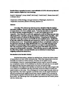
Area-Efficient Linear Regression Architecture for Real-Time Signal Processing on FPGAs Pablo Royer
´ Miguel Angel S´anchez
Marisa L´opez-Vallejo
Carlos A. L´opez Barrio
Dpto. de Ingenier´ıa Electr´onica, ETSI Telecomunicaci´on, Universidad Polit´ecnica de Madrid Ciudad Universitaria s/n, 28040 Madrid, Spain {proyer,masanchez,marisa,barrio}@die.upm.es
Abstract—Linear regression is a technique widely used in digital signal processing. It consists on finding the linear function that better fits a given set of samples. This paper proposes different hardware architectures for the implementation of the linear regression method on FPGAs, specially targeting area restrictive systems. It saves area at the cost of constraining the lengths of the input signal to some fixed values. We have implemented the proposed scheme in an Automatic Modulation Classifier, meeting the hard real-time constraints this kind of systems have.
I. I NTRODUCTION TO L INEAR R EGRESSION Following Moore’s Law, current nanometer technologies have allowed extraordinary integration densities in digital circuits. This has specifically favoured Field-Programmable Gate Arrays (FPGAs), which offer a flexible solution for hardware implementation at a suitable low cost [2]. The flexibility of FPGAs allows the implementation of different generations of a given application and provides space to designers to modify implementations until the very last moment, or even correct mistakes once the product has been released. Furthermore, even though FPGAs are not as efficient as ASICs in terms of performance, area or power, it is true that nowadays they can provide better performance than general purpose CPUs or digital signal processor (DSP) based systems. This fact, in conjunction with the enormous logic capacity allowed by today’s technologies, makes FPGAs an attractive choice for implementation of complex digital systems. Moreover, due to the inclusion of digital signal processing capabilities [3], FPGAs are now expanding their traditional prototyping roles to help offload computationally intensive digital signal processing functions from standard processors. In this context, the implementation of complete signal processing systems in FPGAs has become a reality. FPGAs allow for true parallel processing by supporting multiple simultaneous threads of execution. Typically, the system throughput of many signal processing algorithms can be improved by exploiting concurrency in the form of parallelism and pipelining [4]. However, the complexity of most signal processing algorithms makes the design of this kind of systems complicated and error prone. In this work we have focused on a linear regression method that has been widely used in many signal processing applications, such as [5]–[7]. We have designed an FPGA-oriented architecture that efficiently implements a general linear regression method. The design has been conceived targeting Xilinx devices and with very hard area and performance constraints that other implementations did not meet [8]. The main goals of the proposed architecture are the following: • To make the best use of available resources in order to leave as much free space as possible for other important computations required by the particular signal processing system. • To allow real-time processing: working at the highest possible frequency and with a high degree of parallelism. This work was funded by the CICYT project DELTA TEC2009-08589 of the Spanish Ministry of Science and Innovation.
Fig. 1. Example of a linear regression function and the values from which it is calculated.
The proposed architecture exploits the existence of DSP blocks in current FPGAs to reduce the required distributed logic and provide high performance1 . We have validated our linear regression model by including this module in an Automatic Modulation Classifier (AMC). AMCs identify the modulation format of transmitted signals by observing the received data samples, which are corrupted by the noise and fading channels. AMC plays an important role in civilian and military applications such as software-defined radio, cognitive radio, intelligent modem, dynamic spectrum management, interference identification, electronic surveillance and electronic warfare [9], [10]. The structure of the paper is the following. First, the equations required to compute a general linear regression are formulated. Next, we present the proposed scheme in Section III while the implementation details are provided in Section IV. Finally, experimental results are presented and some conclusions are drawn. II. L INEAR R EGRESSION E QUATIONS As explained, we are searching the linear function that better fits a given set of samples as in figure 1, that is, the coefficients a and b that minimize the mean squared error (MSE): M SE =
N −1 X
(di − a · i − b)2
(1)
i=0
where di is the ith input value (i ∈ {1..N }), a is the slope and b the value at index 0 of the linear regression function. This is achieved using the derivatives: 1 In
particular, we have focused on the Xilinx Virtex-5 SX FPGAs.
i
M SE
N −1 X
=
d2i
N −1 X
2
+a
i=0
+N b2 + 2ab
2
i − 2a
i=0 N −1 X
i − 2b
i=0 N −1 X
i=0
∂M SE ∂a
=
a
2a
b
i=0 N −1 X
i=0 N −1 X
i=0
i=0
=
2N b + 2a N −1 X
=
N −1 X
idi + 2b
idi ACC
di
N −1 X
=
N
N −1 X
i /
i
(3)
i−2
N −1 X
di = 0
a
i=0
i=0 N −1 X
÷ N
b
i −
di
i=0
÷ N
i=0 N −1 X
2
i=0 N −1 N −1 X X
=
i=0 N −1 X 2
2
i /N
(4) Fig. 2.
i
N −1 X i=0 N −1 X
! i ! i
i=0 i=0 N −1 N −1 X X
i −
i −
i=0
di
idi
(5) ! i
i=0 i=0 ! N −1 N −1 X X
i
i=0
i
Example of basic a and b coefficients computation.
results, subtract them and finally a division is performed. Although some operations of this scheme can be performed in a more efficient way, it gives an idea of the workload required to compute a and b coefficients as a direct application of equations 5 and 6. The basic scheme can be significantly improved if the sequence length can be constrained. In order to do that, we can rewrite the equations for the a and b coefficients to separate the part of the equation that depends on the input data, and the part that only depends on the length of the input sequence:
(6)
i=0
=
III. P ROPOSED S CHEME As seen in equations 5 and 6, the coefficients depend on both the input data and the number of input values that is considered. Regarding the input data, two summations are required, one for the values themselves and another one for the values multiplied by their indexes. Concerning the number of values, two more summations are performed, one for the indexes themselves and another one for the squared indexes. In hardware summations are computed by means of accumulators. A fully flexible architecture, that can accept any number of input data, will require to compute the accumulation of the indexes and the squared indexes either as an actual accumulation or with the appropriated formula once we know the final N as in equations 7 and 8, what involves additions or accumulations, and multiplications.
i=0 N −1 X
i
i=0
i 2
=
N2 N − 2 2
=
N3 N2 N − + 3 2 6
� N −1 X N P P · idi N i2 − i i i=0 � � N P −1 X i P 2 P P − · di N i − i i i=0 � � N P 2 −1 X i P 2 P P di · N i − i i i=0 � � N P −1 X i P P P − · idi 2 N i − i i i=0 �
a
which will be used as base in our hardware implementation.
N −1 X
b
!
i=0
N −1 X
ACC
DIVISION
i=0
di − a
idi −
MACC
PRODUCTS AND SUBTRACTIONS
In the end we have:
a
MACC
(2)
i=0
i=0 ! N −1 X 2
!
i=0 N −1 X
i=0
d
i=0
N −1 X
i2 − 2
idi − b
=
∂M SE ∂b
N −1 X
N −1 X
(7)
(8)
In addition, as the denominator in equations 5 and 6 depends on the input, a division is required, that supposes a significant area increase. An example of a basic scheme that performs the linear regression is shown in figure 2, the first stage uses accumulators (ACC) and multiply-accumulators (MACC). The following stages multiply the
b
=
P
(9)
(10)
PNow thePcomputation of a and b is performed by multiplying di and idi –that needed to be calculated in any case– by four constants and then subtracted. The block diagram of the new scheme is now as shown in figure 3, where the number of constants depends on the input sequence lengths we have to consider, and the rate of three or four2 constants per length. IV. I MPLEMENTATION The main advantage of the scheme in figure 3 is that the constants can be stored in a ROM. Even if these constantsPdependP on the value of N we have bypassed the need of computing i and i2 and the division in the hardware, as all these operations are now performed previously at design time. In addition, more area can be saved if we only need to take into account some particular sequence lengths. 2 Two of the values are equal but may be stored with a different binary representation.
i
d
A MACC
B
ACC
X
0 M A:B
0
Y
P
0
C
Z
Fig. 4. MACC
a
Internal architecture of the Virtex-5 DSP48E Slice [3]
Constants
A
b
B Fig. 3.
0 M A:B
0
X
Y
P
Proposed scheme for a and b coefficients computation.
C In our case, we are using a linear regression model for an Automatic Modulation Classifier (AMC). In particular, the linear regression is used in the computation of the key statistics for the detection of phase modulations. The input data is a two sample (phase data) per clock cycle signal of which we do not know the length. To process it, the signal is split into packets of 256 samples that are input to the linear regression module. For long signals this scheme is accurate as at most 255 samples are lost. But for shorter ones, the part of the signal that is lost is not negligible anymore: in some cases even the full signal could be discarded. To avoid this problem we introduce a second linear regression model that takes shorter packets of 128 samples, that halves the maximum number of samples that can be lost, using the scheme explained in section III. The double model is implemented sharing most of the hardware: only new constants have to be stored in the ROM, the rest of the hardware remains unchanged an is limited by the longest model. Our linear regression implementation would be able to deal with any value of N . Nevertheless, there are other limiting modules in the system that impose the restriction of sequence lengths that are powers of two. A. Xilinx DSP48E-based Operators The scheme proposed in figure 3 uses mainly ACCs and MACCs, that makes the Xilinx embedded DSP48E very appropriated for the implementation. A simplified representation of the Xilinx DSP48E architecture [3] is shown in Figure 4 (for instance, internal registers are not drawn). It consists on a 25x18 signed multiplier (ports A and B) followed by a 3-input 48-bit ALU that can be set up as an accumulator. The inputs of the ALU are selected by three multiplexers. If we choose the output of the multiplier only two inputs are allowed, otherwise, if the multiplier is not used, the juxtaposition of A and B ports can be used as a 48-bit input. Other signals that can be input to the ALU are the 48-bit port C or the registered output of the ALU, P. For the implementation of the linear regression two basic operators are required:
0 Z
Fig. 5.
Implementation of a 2-input accumulator using a DSP48E.
ACC We use a DSP48E configured as a 2-input accumulator to P perform the di operation (see figure 5). The two inputs are connected to ports A:B and C, loading the X and Y multiplexers respectively. The output P is connected to the multiplexer Z. P MACC 1 For the idi accumulation shown in Figure 6, three DSP48E are required, two of them performing the multiplications with the samples in ports A and their corresponding indexes in ports B, here the ALU is not required so it is set to add zero. Then, the third DSP48E performs the two-input accumulation. Depending on the area requirement of the design, alternative implementations are possible, like using two DSP48E with one external adder. MACC 2 The following stage, the computation of a and b, is also implemented using one DSP48E. The results of the previous stages (connected to port A) are multiplied by the corresponding constants stored in the ROM (connected to port B) and subtracted by using the ALU. As we only use one DSP48E a and b are calculated one at a time. The implementation is shown in figure 7. B. Accumulators Bit-width Instantaneous phase is the system input (AMC), ranging from −π to π and represented as an 8-bit signed value. We can deduce the integer bits required for the variables in the datapath. The values we are using are unwrapped phases, that can take any value unlike instantaneous phase. The unwrapped phase is inferred from the instantaneous phase as shown in figure 8 to remove phase jumps. Due to the way it is calculated, the most the unwrapped phase can change between two consecutive samples is π so the unwrapped phase
A B
0 M A:B
di
X
Y
0
di,max = π + 2π × i
P A
0
C
Z
A B
0 M A:B
B
C
X
A:B
0
X
Y
P
0 Z
Y
0
0 M
5π 3π π
P
0
C
0
Z
Fig. 9.
1
TABLE I ROM CONTENTS coeff.
B
C
0 M A:B
0
X
a b
Y
i
Maximum unwrapped decimated phase achievable.
Fig. 6. Implementation of a 2-input multiply-accumulator using three DSP48E.
A
3
2
factor P idi P di P idi
128 model 5.7224 · 10−6 · 234 3.6337 · 10−4 · 228 3.0887 · 10−2 · 222 3.6337 · 10−4 · 228
256 model 7.1527 · 10−7 · 237 9.1196 · 10−5 · 230 1.5534 · 10−2 · 223 9.1196 · 10−5 · 230
P variables can reach are computed as:
0 Z
X
di
255 X (2i + 1)π
=
±
= =
±65536π 255 X ± i(2i + 1)π
=
±11152000π
i=0
Fig. 7.
How to calculate the a and b coefficients using one DSP48E.
X
idi
(11)
i=0
will range from −512π to 512π and will require 9 + 8 = 17 bits. The reason behind this is that we take 512-sample packets that are then decimated: we only take even samples resulting in 256-sample packets. As the unwrapped and decimated phases di cannot reach the maximum value until the end of the packet, P according P to figure 9, the maximum and minimum values that the di and idi intermediate
di
π -π Fig. 8. Unwrapped phase, and instantaneous phase (dashed) from which it is inferred.
(12) P so we need p8 + log2 65536q = 24 integer bits to represent di P and p8+log2 11152000q = 32 integer bits to represent idi . Since the instantaneous phase only has integer bits, neither the unwrapped phase nor the summations have fractional bits. Those results correspond to the 256-sample model, the same procedure is used to obtain the results for the 128-sample model. C. ROM Constants P P The idi and di accumulations have to be multiplied by one of the constants stored in the ROM. Then the results are subtracted two by two to obtain the a and b coefficients. As we are using the DSP48E multiplier to perform this operation we have to choose between the 18-bit or the 25-bit input. The best selection is to use the 18-bit input for the constants stored in the ROM and the 25-bit input for the results of the accumulations. The reason behind this is that since the constants do not depend on the input and are calculated during the implementation, we can make sure that the 18 bits that we are using are significant. On the other hand, the number of significant bits of the results of the accumulations depend on the input data, and some of the bits may not be meaningful. So it is better to use the multiplier largest input for these values. Table I shows the values of these constants as well as the number of bits they have to be shifted to be represented as an 18-bit integer with all the bits being significant.
D. Aligning the products P The idi accumulation is represented with more than 25 bits, that is the maximum input the multiplier we are using can manage. So the lowest bits have to be discarded, that is 7 bits for the 256 model. The error produced by this truncation will be calculated later. We have to make sure that the two results of the multiplication of one of the constants on table I by one of the accumulations are aligned so that they can be subtracted. P P We discard the 7 lowest bits of idi and leave di as it is: X −7 37 −7 7.1527 · 10 · 2 × idi · 2 X −5 30 −9.1196 · 10 · 2 × di = a256 · 230 −2
23
−9.1196 · 10−5 · 230
1.5534 · 10
·2
= b256 · 223
(13) ×
X
di
×
X
idi · 2−7 (14)
If we share the hardware for more than one model, there are two alternative architectures at this point: 1) For the first option, the accumulations are switched by a different amount of bits depending on the model. With this scheme we obtain the highest precision, as least bits as possible are discarded, at the cost of a larger area. 2) For the second option, the results of the accumulations are input directly to the multiplier without taking into account the model they come from. With this scheme we obtain the smallest area since the number of discarded bits does not depend on the model, avoiding the need of a multiplexer. On the other hand we obtain a lower precision since we discard more bits than necessary. This gets worse if we use models shorter than 128. Another minor cause why we loose precision is by the constants stored in the ROM that use less significant bits than they could to keep the results aligned. E. Results Bit-width The a and b coefficients depend on several factors that are also dependent on one another. Therefore it would be difficult to deduce their range from the equations used to calculate them. But knowing that a represents the slope of the interpolated linear equation and that the most the unwrapped phase can grow on a single step is π, after the decimation –we keep only one sample out of two so the maximum growth is doubled– we can say the a will range from −2π to 2π and therefore will have 9 integer bits. a has 30 fractional bits, as can be deduced from P the equation 13. However due to the bits that are discarded from idi not all these bits are meaningful. After discarding bits, the maximum error that the resulting value may have is one unit, from how the a coefficient is calculated, this error at the input becomes an error of 7.1527 · 10−7 · 237 = 9.8306·104 at the output, that is 16.6 bits. We can say that the coefficient a can be represented with 9 integer bits with at least 13 fractional bits, this corresponds to a resolution of 7.2275 · 10−7 · π. The range of b depends on the indexes we take since b is the value that the interpolated function takes for i = 0. In our case, with i ranging from 0 to 255 it seems that the highest value that b can take is ±128π that corresponds to a pyramid-shaped input function as shown in figure 10. This corresponds to 15 integer bits for the 256 model. From equation 14, b will have 23 fractional bits. But again not all these bits are meaningful. As for a we can calculate the highest error
di 255π 128π π 0
i 128
255
Fig. 10. The input data (dashed) and the corresponding interpolated function (continuous) y = b with the highest possible value for b.
as 9.1196 · 10−5 · 230 = 9.7921 · 104 or 16.6 bits for the 256 model. The coefficient b can be represented with 15 integer bits and at least 6 fractional bits, with a resolution of 9.2512 · 10−5 · π. Although from the number of fractional bits, it seems that coefficient b is less accurate than a, the fact that a is a slope that will be multiplied by an index makes the error to increase while b is a constant that is always added without any scaling and the error remains constant. The constants stored in the ROM also lead to an error due to the rounding that is made to make them fit in an 18-bit representation. This results in a random error as it depends on the input. This error should be calculated with simulations. F. Control The input interface consists on two ports to receive the samples at the rate of two per clock cycle as explained before, and two control signals, one in charge of indicating when a new sequence starts, and the other indicating the length of the sequence and therefore the model —256 or 128 samples— that has to be applied. The control resets the accumulators when a new sequence starts and counts the number of samples received, when the expected number of samples have been processed it loads the results of the accumulators. With those results a second state machine is started that uses the appropriated constants depending on the model to infer the coefficients of the linear regression. As soon as a sequence has been input a new one can start, achieving a continuous flow of input blocks. This way the first stage is computing the accumulation while the next stage computes the coefficients of the previous sequence. The latency of the first stage depends on the number of samples, while the second stage has a fixed latency that depends on the implementation, in our case five cycles. The latency of the second stage is the one that would limit the minimum number of samples of a sequence. V. R ESULTS Three schemes proposed in previous sections have been implemented in a Xilinx Virtex5 XC5VSX95T-2 FPGA obtaining the results presented in table II. All the results presented in this section include both the area of the data-path as well as the control logic in charge of counting the number of samples, loading the results when the the expected length of the input signal has been received and starting the computation of the coefficients. The implemented schemes have consisted on: • A linear regression using only the 256-sample model.
TABLE II R ESULTS Model 256 256 & 128
Discarded bits depend on the model same for both models
Area 66 sl. & 5 dsp 89 sl. & 5 dsp 70 sl. & 5 dsp
Freq. 458 MHz 385 MHz 439 MHz
A linear regression using both 128 and 256-sample models, discarding different amounts of bits from the initial summations depending on the model as explained in section IV-D-1. • A linear regression using both 128 and 256-sample models, discarding the same bits from the initial summations as explained in section IV-D-2. The number of samples could have been any other and would have only meant a change in the constants stored in the ROM and in the sample counter. There is no restriction in the hardware that implies a power of two number of samples. The base of the three implementations is the one that only has the 256-sample model. All the arithmetic computation is carried out by the 5 DSP48E, the 66 slices are due to the ROM and the control: mainly P an index P counter and a multiplexer to choose which summation ( di or idi ) is input the the DSP48E that calculates the a and b coefficients. The estimated frequency this implementation can achieve is 458 MHz. Adding the 128-model to the previous implementation does not increase the number of required DSP48E as the arithmetic computation is the same, the difference is made in the state machine –that has to be aware of the model we are using– and in the ROM –that has to store more coefficients. The implementation with a double model (128 and 256 samples) and discarding the same amount of bits from the summations results on an increase of the area of only 4 slices (6.1%). The estimated maximum frequency remains almost the same: 439 MHz. The implementation of the double model but discarding the least significant bits as possible from the summations leads to a larger area: 89 slices, an increase of 27% relative to the other doublemodel implementation. This increase is due to the multiplexers that choose which summation is input to thePDSP48E that computes P the coefficients, from two inputs (one for idi and one for di ) in P the P previous implementation to four inputs (two for idi and two for di ) as each summation has to be input with a different shifting depending on the model. The maximum frequency achievable by this implementation is also decreased when compared with the other implementations: 385 MHz, as the critical path is in the new four input multiplexer. This can be solved, if necessary, by introducing new registers. Only one DSP48E is used to compute coefficients a and b from the different summations, this is done as a subtraction of two products for each of the coefficients. As a consequence, the minimum input •
signal length would be one that lasts 4 clock cycles. In our case, at the rate of two sample per cycle this corresponds to an 8-sample length signal. VI. C ONCLUSION The coefficients obtained by a linear regression are widely used in many signal processing applications. For instance, linear regression is the base of the calculation of the statistics an AMC computes to infer the modulation that a signal has, as well as to determine some of the parameters of this modulation. The linear regression hardware does not represent a large area when compared to the vast resources current FPGAs provide. However, as the number of these modules a digital signal processing system can be made of, decreasing their area can and improving their working frequency results in a great enhancement of the whole system. In this work we have proposed FPGA-oriented architectures for the implementation of different linear regressions, showing that large area savings can be achieved if we reduce the possible input signal lengths to some unconstrained predefined values. Furthermore, experimental results show that hard real time constraints can be met when using these modules in a complex AMC system. R EFERENCES [1] R. Tessier and W. Burleson, “Reconfigurable computing for digital signal processing: A survey,” The Journal of VLSI Signal Processing, vol. 28, no. 1, pp. 7–27, 2001. [2] T. Todman, G. Constantinides, S. W. O. Mencer, and W. L. P. Cheung, “Reconfigurable computing: architectures and design methods,” IEE Proc. Computers and Digital Techniques, vol. 152, no. 3, pp. 193–207, March 2005. [3] Xilinx Corporation, “Virtex-5 FPGA XtremeDSP Design Considerations,” http://www.xilinx.com/support/documentation/user guides/ ug193.pdf, September 2008. [4] K. Parhi, Digital Signal Processing Systems-Design and Implementation. John Wiley & Sons, 1999. [5] S. Tretter, “Estimating the frequency of a noisy sinusoid by linear regression (Corresp.),” Information Theory, IEEE Transactions on, vol. 31, no. 6, pp. 832–835, 1985. [6] J. Grajal, O. Yeste-Ojeda, M. S´anchez, M. Garrido, and M. L´opezVallejo, “Real Time FPGA Implementation of an Automatic Modulation Classifier for Electronic Warfare Applications,” in 19th European Signal Processing Conference, 2011. [7] D. Yang, H. Li, G. Peterson, and A. Fathy, “Compressed sensing based UWB receiver: Hardware compressing and FPGA reconstruction,” in Information Sciences and Systems, 2009. CISS 2009. 43rd Annual Conference on. IEEE, pp. 198–201. [8] D. Yang, G. Peterson, H. Li, and J. Sun, “An FPGA implementation for solving least square problem,” in 2009 17th IEEE Symposium on Field Programmable Custom Computing Machines. IEEE, 2009, pp. 303–306. [9] E. Azzouz and A. Nandi, “Automatic modulation recognition–I,” Journal of the Franklin Institute, vol. 334, no. 2, pp. 241–273, 1997. [10] O. Dobre, A. Abdi, Y. Bar-Ness, and W. Su, “Survey of automatic modulation classification techniques: classical approaches and new trends,” Communications, IET, vol. 1, no. 2, pp. 137–156, 2007.