1This work in supported in part by Qualcomm, SRC grant, NSF 1147388,. 0903432 and by DoE ... ory technologies to improve the bandwidth of caches with.
Bandwidth-Aware Reconfigurable Cache Design with Hybrid Memory Technologies Jishen Zhao, Cong Xu, Yuan Xie Computer Science and Engineering Department, Pennsylvania State University {juz138,czx102,yuanxie}@cse.psu.edu Abstract—In chip-multiprocessor (CMP) designs, limited memory bandwidth is a potential bottleneck of the system performance. New memory technologies, such as spin-transfer torque memory (STT-RAM), resistive memory (RRAM), and embedded DRAM (eDRAM), are promising on-chip memory solutions for CMPs. In this paper, we propose a bandwidth-aware reconfigurable cache hierarchy (BARCH) with hybrid memory technologies. BARCH consists of a hybrid cache hierarchy, a reconfiguration mechanism, and a statistical prediction engine. Our hybrid cache hierarchy chooses different memory technologies to configure each level so that the bandwidth provided by the overall hierarchy is optimized. Furthermore, we present a reconfiguration mechanism to dynamically adapt the cache space of each level based on the predicted bandwidth demands of different applications, which is guaranteed by our prediction engine. We evaluate the system performance gain obtained by our method with a set of multithreaded and multiprogrammed applications. Compared to traditional SRAM-based cache designs, our proposed design improves the system throughput by 58% and 14% for multithreaded and multiprogrammed applications, respectively.1
I. I NTRODUCTION One critical bottleneck for chip-multiprocessor (CMP) performance scaling is the widening gap between the increasing bandwidth demand created by processor cores and the limited bandwidth provided by off-chip memories [1]–[3]. Due to such limitation, memory-demanding applications with a large working set spends additional cycles on off-chip memory accesses, and thus decreases the parallelism. In addition, even moderately memory-demanding applications will reach the bandwidth limitation as the number of cores scales up [4]. Consequently, memory bandwidth becomes one of the most important factors that influence high performance system design. Various techniques can be found in recent computing systems and research work to address the memory bandwidth challenges. High performance computing systems such as NVIDIA’s Tesla [5] rely on extremely high main memory bandwidth provided by the graphics DDR (GDDR) memory to satisfy the demand of large number of processor cores. However, GDDR memory runs at high clock rates and consumes more power than conventional DRAM modules. It is undesirable for either general purpose or high performance computing systems to improve their computing performance by simply sacrificing power efficiency. With the emerging 3D integration technology, memories can be stacked on top of processor cores to provide high memory bandwidth [6]. 1 This work in supported in part by Qualcomm, SRC grant, NSF 1147388, 0903432 and by DoE under Award Number DE-SC0005026.
However, the placement of through-silicon-vias (TSVs) and the thermal problem are still open questions for 3D IC design. Caching is known to be the most effective approach to reduce memory access latency. Proper cache hierarchy design can also help mitigate the increasing pressure to off-chip memory bandwidth. With an extensive study on limited pin bandwidth in multiprocessor systems, Burger et al. concluded that on-chip cache with more levels would improve the system performance [2]. Rogers et al. explored the requirements of on-chip cache hierarchy and optimization techniques due to scaling of processor core numbers [3]. Both studies show that exploring on-chip memory hierarchy in a manner focusing on bandwidth optimization will benefit future computing systems in terms of performance scaling. On-chip memory with fast random access, high storage density, and non-volatility becomes possible as the emergence of various new memory technologies, such as spin-transfer torque memory (STT-RAM), phase-change memory (PCRAM), and resistive memory (RRAM). These new memory technologies have been proposed to be promising solutions for on-chip caches [7]. In this paper, we propose a novel bandwidthaware reconfigurable cache hierarchy (BARCH) to enhance system performance of CMPs with these emerging memory technologies. Our goal is to improve the memory system with regard to bandwidth optimization by devising a hybrid cache hierarchy. The contributions we present in this paper include: • Demonstration of the feasibility of using emerging memory technologies to improve the bandwidth of caches with large capacities. • A bandwidth-aware hybrid cache hierarchy with optimized overall bandwidth. The hybrid cache design is motivated by the observation that one memory technology may provide higher bandwidth than others in certain range of capacities, but not a single memory technology maintains the highest bandwidth over the entire range of capacities. • A run-time cache reconfiguration mechanism that dynamically adapts the cache space of each level according to the bandwidth-demanding variations of applications. • A probability-based prediction engine that facilitates the reconfiguration mechanism. The prediction engine estimates the bandwidth demand of an application based on statistical history information stored in a pattern table. II. BACKGROUND AND R ELATED W ORK Memory bandwidth The bandwidth problem of multicore processors has drawn much attention recently. Yu et al.
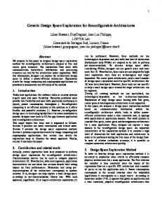
Fig. 1. Overview of the hardware configuration. (a) Configuration of reconfigurable hybrid cache hierarchy. (b) The overall bandwidth-capacity curve of the hybrid cache hierarchy (a generic case of Figure 3).
proposed a last level cache (LLC) partitioning algorithm to minimize bandwidth requirement to off-chip main memory [8]. Cache resources were allocated for the target workload in a way to reduce the overall system bandwidth requirement by considering memory bandwidth demand for each task. One key insight in their work was that cache miss rate information might severely mis-represent the actual bandwidth demand of a workload. Thus the overall system performance and power consumption might be inappropriately estimated. However, they only focused on LLC (L2 cache). Our design target is the overall on-chip memory hierarchy, which provides more design dimensions and flexibility. Furthermore, the cache partition in [8] was determined offline, and remained fixed during run-time. We will present a reconfiguration mechanism to dynamically adapt the space of each cache level to the demand of different applications. Emerging memory technologies STT-RAM is the subsequent technology of magnetic RAM (MRAM). STT-RAM employs Magnetic Tunnel Junction (MTJ), which contains two ferromagnetic layers and one tunnel barrier layer, as its binary storage. RRAM is another emerging non-volatile memory. In RRAM, a normally insulating dielectric is conducted through a filament or conduction path generated by applying a sufficiently high voltage. The filament may be reset or set by applying an appropriate voltage. One concern for non-volatile memories is their endurance. The endurance of STT-RAM is larger than 1015 [9]. The endurance of RRAM is in the range of 105 to 1010 [10]. Therefore, STT-RAM is a practical solution for cache design, while RRAM is feasible for LLC with low write intensity. Large amount of recent research focused on exploring new memory technologies to balance between latency, bandwidth, and cost. Various memory technologies - SRAM, eDRAM [9], and STT-RAM [11] were explored as L3 caches to improve system performance and power consumption. These studies mainly focused on reducing the latency gap between L2 cache (LLC) and external memory. However, the bandwidth bottleneck issue was not addressed in all these work. Reconfigurable cache A number of proposals have been made for reconfigurable cache designs targeted at performance
optimization [12], [13]. In Ranganathan et al.’s study, cache memory resources are dynamically divided into multiple partitions used for different processor activities, e.g., instruction reuse [12]. A recent work proposed to adapt the cache hierarchy topologies to workload cache access behaviors at run-time [13]. Both studies explore the performance benefits by minimizing memory access latency, and do not consider memory bandwidth requirement. The insight of our study is that design optimization targeting at minimizing the demanded off-chip memory bandwidth can boost system performance in terms of instruction execution throughput. Predictor design Efficient application behavior predictions are critical to performance of reconfigurable architectures. Zhou et al. monitored memory access patterns and estimated memory behavior of workloads for energy efficient memory allocation [14]. Kim et al. [15] proposed to examine cache miss at each time interval, and reconfigure cache partitioning based on current memory access pattern. However, their approach cannot track long term and variable memory access patterns. Duesterwald et al. described different statistical and table based predictors for within- and across-metric predictions of performance monitoring information [16]. They showed that the table-based predictor generally outperforms the other predictors they tested. Sarikaya et al. described an optimal prediction technique based on a predictive least squares minimization [17]. Recently, they showed the benefit of statistical metric modeling for tracking varying pattern history lengths and modeling long term patterns [18]. In this work, we employ a prediction engine which consists of multiple-level statistical predictors to facilitate the on-chip memory reconfiguration. III. BANDWIDTH -AWARE R ECONFIGURABLE C ACHE H IERARCHY While many design methods involved with new memory technologies endeavor to reduce the off-chip memory access latency, our work focuses on decreasing off-chip bandwidth demand by employing hybrid on-chip memory hierarchy and reconfiguration. Figure 1(a) depicts an overview of our BARCH design. We examine different memory technologies in terms of read and write access latencies, dynamical energy, and bandwidth under dynamic energy constraint. The bandwidth-
4 2 0
Capacity
eDRAM
STT-RAM
RRAM
8 6 4 2 0
(b)
Capacity
SRAM
STT-RAM
RRAM
eDRAM
4 2 0 -2 -4
64KB 128KB 256KB 512KB 1MB 2MB 4MB 8MB 16MB 32MB 64MB 128MB 256MB 512MB 1GB
6
(a)
SRAM
ln ( D y n a m ic E n e r g y ) , n J
RRAM
ln ( La t e n c y ) , n s
STT-RAM
64KB 128KB 256KB 512KB 1MB 2MB 4MB 8MB 16MB 32MB 64MB 128MB 256MB 512MB 1GB
eDRAM
64KB 128KB 256KB 512KB 1MB 2MB 4MB 8MB 16MB 32MB 64MB 128MB 256MB 512MB 1GB
ln ( R e a d La t e n c y ) , n s
SRAM 8
(c)
Capacity
Fig. 2. Latency and dynamic energy of different memory technologies. (a) Read latency. (b) Latency with 40% of write intensity. (c) Dynamic energy with 40% of write intensity.
capacity curves of different memory technologies are shown in Figure 1(b). In a given range of capacities, one memory technology may provide the highest bandwidth. However, we cannot find a single memory technology that always maintain the highest bandwidth over the whole range of capacities. Based on this observation, we employ hybrid memory technologies in BARCH. At each level of cache, we select the memory technology which provides the highest bandwidth within a specific capacity range. The overall bandwidth-capacity curve of BARCH is maintained to be the highest across the whole capacity range, shown in the solid curve in Figure 1(b). In order to integrate different memory technologies in a single processor, 3D memory stacking technique [9] may be employed. Since this paper focuses on studying the architectural design to overcome the memory bandwidth bottleneck, we will not discuss the detailed implementation method. In addition, we dynamically adapt the cache hierarchy according to the bandwidth demand of different applications. The total cache space at each level is partitioned to a set of fast ways and slow ways. During run-time, we examine the bandwidth demand of individual application at each execution time interval. Cache space at each level is tailored according to the bandwidth demand. In order to facilitate the reconfiguration, we design a statistical prediction engine to collect the bandwidth demands of applications at the end of each execution time interval, and predict the bandwidth demands for the next time interval. Rather than conventional last value or history table based predictors, we present a probabilitybased statistical predictor which can achieve high accuracy with small performance and area overhead. A. Hybrid Cache Hierarchy First of all, we examine the latency, dynamic energy, and bandwidth of different memory technologies including SRAM, STT-RAM, RRAM, and eDRAM. Since PCRAM has serious endurance issue, we do not consider it as an on-chip memory candidate. We use NVsim [19], a circuit level performance, energy, and area estimation tool, to evaluate different memory technologies. Latency The read and write latencies of the two NVMs, STTRAM and RRAM, are asymmetric. The write latency is much higher than read. Therefore, we consider the read and write latencies separately. The read latency (dr ) is evaluated using
the following equation: dr = dHti + dwl + dbl + dcomp + dHto
(1)
where dHti and dHto are H-tree input and output delays that determined by the RC delay of global wires, dwl is decoder and word-line delay, dbl is bit-line and sense amplifier delay, dcomp is comparator delay related to the read noise margin of memory cell that is affected by off/on resistance ratio, and dHto is H-tree output delay. Figure 2(a) illustrates the read latency of different memories as a function of memory capacity with both x- and y-values in log scale. Sensing delay dominates the read latency of the two NVMs at small capacities. Therefore, STT-RAM and RRAM do not show any advantages in read latency. When H-tree delay unveils at large capacities, RRAM (with the smallest cell size) becomes faster than other memory technologies. The read latency of SRAM will increase rapidly after 128MB due to the large area. The write latency of NVMs is dominated by the write pulse width. We evaluate the write pulse of 10ns, 20ns, and 100ns for STTRAM and RRAM. When the cache size is small (less than 4MB), the write latency of the two NVMs are much higher than SRAM and eDRAM. As the capacity grows to larger than 128MB, the write latency of SRAM becomes higher than the NVMs again due to the large area. Fortunately, the write intensity of most applications is lower than 40%. We inject 40% of write intensity, and obtain the latency curves of different memory technologies as shown in Figure 2(b). The curves meet each other at different capacities. The key observation is that the latency benefit of STT-RAM, eDRAM and RRAM starts to show at large capacities. We examine the latency curves with other write intensities, and observe similar pattern. Dynamic energy Figure 2(c) demonstrates the dynamic energy of different memory technologies with 40% write intensity. The first crossing point locates between SRAM and STTRAM at the capacity around 2MB. STT-RAM consumes lower dynamic energy than SRAM after this crossing point. The crossing point between SRAM and eDRAM is around the capacity of 16MB. The dynamic energy of RRAM keeps high until hits the curve of the SRAM at the capacity of 1GB. Bandwidth under energy constraint We estimate the read and write bandwidths that can be provided by different memory technologies based on our latency and dynamic energy evaluations. The access power of a cache is approximately
STT-RAM
RRAM
eDRAM
15 10 5 0
64KB 128KB 256KB 512KB 1MB 2MB 4MB 8MB 16MB 32MB 64MB 128MB 256MB 512MB 1GB
ln ( B W ) , M B /s
SRAM
Capacity
Fig. 3. Bandwidth-capacity curves of different memory technologies under dynamic energy constraint (with 40% of write intensity).
√ proportional to bandwidth × capacity [20]. Figure 3 shows the bandwidth curves estimated under the energy constraint based on this relationship. In this figure, the curves meet each other at different memory capacities. For example, the curves of SRAM and STT-RAM cross each other at around 2MB, and eDRAM provides the highest bandwidth after 16MB. Therefore, a single technology can provide the highest bandwidth within a given range of memory capacity. Based on our evaluation of latency, energy, and bandwidth of different memory technologies, we select SRAM, STT-RAM, and eDRAM to construct our hybrid cache hierarchy. We discard RRAM due to its high dynamic energy and low endurance. As shown in Figure 1(a), the baseline CMP system consists of multiple cores, where the L1 caches are private to each core and the lower level caches are shared by the cores. With the bandwidth-capacity curves of various memory technologies, we can optimize the bandwidth provided by the cache hierarchy with hybrid memory technologies. To achieve this goal, we configure the cache hierarchy based on the following factors: a) Number of levels: Figure 1(b) is a sketch of Figure 3. In our case, “Mem Tech” 1, 2, and 3 are SRAM, STTRAM, and eDRAM respectively. We can observe two crossing points (SRAM and STT-RAM, STT-RAM and eDRAM) of the bandwidth-capacity curves, dividing the capacity range into three regions. Based on this observation, we configure the shared cache hierarchy as three levels. Each level of cache is implemented with the memory technology that provides the highest bandwidth in a specific capacity range. As a result, the overall bandwidth-capacity curve of the shared cache hierarchy is the solid curve (“Hybrid”) in Figure 1(b). b) Memory technology of each level: At each cache level, we select the memory technology providing the highest bandwidth within the range of capacities between the two crossing points in bandwidth-capacity curve. In our case, SRAM, STT-RAM, and eDRAM are selected as the L2, L3, and L4 caches respectively. c) Capacity of each level: The total capacity of each level is determined by the crossing point of the bandwidth curve of two memory technologies. For example, the overall capacity of SRAM/L2 is 2MB, since the curves of SRAM and STT-RAM meet between the capacities of 2MB and 4MB. The total capacity of STT-RAM/L3 is 16MB. We limit the capacity of eDRAM/L4 to be 64MB to avoid high area and energy
overhead. Each level of cache is configured to be multiple banks the same way as the conventional cache design. The goal of such design is to leverage different memory technologies to configure an on-chip memory system with optimal available bandwidth at different capacities. The on-chip memory system will therefore always keep high bandwidth over the whole range of capacities. B. Reconfiguration Although the above hybrid memory configuration maintains the optimal provided bandwidth over the whole range of capacities, it does not guarantee the best performance of different applications with a variety of bandwidth demands. Smaller caches provide higher bandwidth. However, the smaller the capacity, the less proportion of the working set can be fit into such limited cache space. As a result, the application may create very high bandwidth demand to the next level of cache. Consequently, we reconfigure the each level of caches at runtime adaptive to the bandwidth demands and the working set sizes of different applications, and balance the available and demanded bandwidth at each cache level. In order to reconfigure the cache spaces, we further divide the overall cache space at each level into a set of fast ways and slow ways, which are defined as “partitions”. The faster partitions will provide higher bandwidth, but smaller capacities. During system initialization, we configure the cache system to provide the highest available bandwidth. Only the fastest partitions are activated. The rest of the cache space is sent into drowsy state [21]. During run-time, we re-adjust the cache capacities, and activate the slower partitions according to the demand bandwidth of specific applications. The bandwidthcapacity curve of the hybrid cache hierarchy appears to be monotonically decreasing as depicted in Figure 1(b). At a specific time point, the demanding bandwidth of an application at each cache level can be mapped to a single point on the curve. Accordingly, we can reconfigure each level of cache to the available size that is the closest to the capacity point corresponding to the demanded bandwidth. Reconfiguration is applied at the end of each evaluation time interval. The length of the time interval can be fixed, or depends on the operating system context switch. At the end of a time interval, we determine the upper bound of the capacity at cache level-i (sui ) by mapping the demand bandwidth (DBW) of a specific application to the hybrid cache hierarchy’s bandwidth-capacity curve, i.e., sui = f −1 (DBWi ) where f (x) represents the bandwidth-capacity relationship of the hybrid cache hierarchy. DBW is measured by miss per second at previous level of cache, i.e., Cm Bl /t where Cm and Bl are number of cache miss and cache line size respectively. DBWi is generated using the prediction engine, which will be presented in section III-C. In theory, higher bandwidth provided by the memory system increases both the throughput and power consumption of computing systems. Therefore, we define a lower bound to the capacity of cache level-i as sli = f −1 (DBWi ∗ (1 + σ)), where σ is a pre-defined threshold to constrain the provided bandwidth with limited power overhead. The capacity of cache level-i (si ) is thus
Algorithm 1 Statistical prediction algorithm Input: The new demand bandwidth sample w˜i in time interval i. Output: The prediction of demand bandwidth wi+1 in the next time interval i + 1. 1: Normalize the new sample to one of quantization bins as wi ; i−1 i 2: Update the two counters c(wi−2 ) and c(wi−2 ) with wi ; 3: if !hitPattern(s ← wi−l+1 ..wi ) then 4: Add an new entry s into pattern table; i−1 i 5: p(s) ← calcP robability(s, c(wi−2 ), c(wi−2 ); 6: else i−1 i 7: p(s) ← calcP robability(s, c(wi−2 ), c(wi−2 ); 8: end if 9: k ← indexOf M axP robability(p) 10: wi+1 ← patternT able[k][l]
selected in the range of sli ≤ si ≤ sui . In addition, one or more partitions at cache level-i can be configured to become level-i.5 as shown in Figure 1(a). This may happen when the demand capacity at cache level-(i+1) is detected to be smaller than the available free space at level-i. In this case, the primary miss path at level-i is re-directed to level-i.5. Our reconfigurable design exploits set associativity in conventional cache organizations. One merit of such design is the trivial modification to existing cache architecture, since the division of ways already presents in a conventional cache organization. An n-way set associative cache consists of n data and tag arrays. We divide the each level of cache into partitions of fast ways and slow ways at the granularity of the k-ways, where k is determined by the available capacity range of the cache level. Reconfiguration will not affect the bits of the address fields that are used as tag, index, and block offset bits. Modifications to the conventional cache architecture include: • Memory status vector A set of memory status vectors are stored in each level of cache. A single 2-bit entry in the vector represents the current status of the corresponding partition (active, drowsy, or configured as level-i.5). • Input and output paths The input and output data paths are duplicated to accommodate multiple active partitions in a single cache level. • Additional multiplexors Additional wiring and multiplexors at address decoders and tag comparators are also required to support the reconfiguration. C. Prediction Engine Memory reconfiguration relies on accurate predictions of bandwidth demand of a workload to address the dynamically varying application characteristics. Conventional last value or table based predictors can model neither long range patterns of an application nor patterns with variable lengths. In this work, we employ a statistical predictor to support the BARCH design. The basic idea of the predictor is similar to the nGram models, which are typically used by speech and natural language processing [22]. The n-gram models are usually formulated as a probability distribution p(s) over a sequence of strings s, and attempt to reflect how frequently s occurs as a sentence. Prediction on a reasonable combination of strings is then generated based on the probability distribution. Our predictor employs the same basic idea, but with significantly
TABLE I P REDICTION ACCURACY FOR DIFFERENT WIDTHS OF THE PATTERN TABLE
Benchmark canneal facesim streamcluster astar bwaves gamess GemsFDTD lbm mcf perlbench wrf zeusmp
Width of Pattern Table 10 9 8 34% 34% 33% 30% 21% 19% 44% 42% 40% 100% 100% 37% 100% 100% 31% 100% 100% 100% 100% 100% 100% 100% 100% 56% 100% 100% 97% 100% 100% 100% 100% 100% 100% 100% 100% 100%
12 100% 98% 100% 100% 100% 100% 100% 100% 100% 100% 100% 100%
7 31% 15% 33% 31% 35% 100% 100% 62% 49% 100% 100% 100%
different implementation details. While language modeling is built from a set of previous collected training sentences with finite lengths, our statistical model needs to be able to dynamically generate predictions based on a continuous sequence of metrics. In addition, we can only implement limited resolution for the metrics. Therefore, we need to normalize the demanded bandwidth values with a limited number of quantization bins. In our model, each demanded bandwidth (DBW) sample obtained in a time interval is analogous to a string in language, and a given length (the “order”) of samples is stored in a table as a pattern. At each time interval, the prediction engine will update the pattern table with the new DBW sample, and calculate probability of the updated pattern. Using the chain rule, the probability of a pattern s of length l can be calculated without loss as the product of conditional probabilities as the equation shown below. p(s) = p(w1 )p(w2 |w1 )...p(wl |w1 ...wl−1 )
(2)
where wl is the DBW sample obtained in current time interval, and w1 through wl−1 are the preceding l − 1 DBW samples. Equation 2 can be represented as p(s) =
l Y
p(wi |w1 ...wi−1 )
(3)
i=1
In n-gram models, we make the approximation that each conditional probability only depends on the preceding n − 1 samples and obtain the following equation. p(s) =
l Y
i−1 p(wi |wi−n+1 )
(4)
i=1 i−1 in which wi−n+1 denotes the sequence of wi−n+1 ...wi−1 . In order to compute the result of Equation 4, an estimation of i−1 of p(wi |wi−n+1 ) can be generated using maximum likelihood estimation (MLE). In n-gram models, the widely-used largest n is n=3, and induces a trigram model. We evaluate the prediction accuracy with different n values, and demonstrate
Fig. 4. Components of prediction engine and the prediction control flow. (a) Components of the prediction engine include the pattern table, the probability vector, and an array of counters. (b) The control flow of the prediction engine.
that the trigram model can achieve reasonable high accuracy. Therefore, we adopt n=3 in our predictor. Each conditional probability is calculated using MLE in Equation 5. i−1 pˆ(wi |wi−n+1 )=
i c(wi−2 ) i−1 c(wi−2 )
(5)
where c(wab ) is the number of times that the sequence wa ..wb appears in preceding samples. The bandwidth demand of the next time interval is predicted to be the last value in the pattern with the highest probability. Figure 4(a) shows the hardware components of our prediction engine, which includes a pattern look-up-table, a probability vector, and a set of counters. The prediction algorithm is described in Algorithm 1. The predictor can catch a pattern of different lengths. As shown in Figure 4(a), all the shaded entries in the pattern table can be prediction candidates. If the predictor cannot match a pattern of the maximum available length, it will try to match the patterns with lower orders. 1) Prediction accuracy: Table I lists the accuracy of the prediction engine applied to both multithreaded and singlethreaded benchmarks. The DBW values are normalized using 20 quantization bins. Based on our evaluation, the primary parameter that affect the prediction accuracy is the width (order) of the pattern table. By storing longer patterns, the predictor is less likely perturbed by a single deviated sample. As illustrated in Table I, our predictor achieves almost 100% accuracy with the order of 12. Multithreaded applications, such as canneal, facesim, and streamcluster, tend to favor higher orders than single-threaded benchmarks. Even with the order of 9, the predictor is still 100% accurate with 9 out of 12 benchmarks. 2) Storage overhead: Wider pattern tables lead to higher prediction accuracy, but also incur more storage and performance overhead. To balance between the prediction accuracy and the overhead, we configure the width of the pattern table at each cache level to be 12, which guarantees almost 100% prediction accuracy with most of the applications. Each probability entry is a 64-bit floating point value. The counter
array is 3-byte wide. The lengths of the pattern table and counter array are fixed to 240. The storage overhead at each cache level is listed in Table II. The prediction engine requires only 6KB of storage at each cache level. TABLE II S TORAGE OVERHEAD OF THE PREDICTION ENGINE .
Component Pattern Table Probability Vector Counter Vector
Width 12-byte 8-byte 3-byte
Length 240 240 240
Storage 3KB 2KB 1KB
3) Computational overhead: The computational complexity of our prediction algorithm is O(ql), where q is the number of quantization bins. The computational time of generating a prediction is bounded by the size of the pattern table and the limited quantization bins. The overall computational overhead is constrained to be on the order of microseconds. Therefore, the prediction algorithm can be implemented by operating system during context switch without explicit performance overhead. IV. E XPERIMENTS In this section, we show experimental results for system performance improvement with the our novel BARCH design. A. Experimental Setup We use Simics [23] as the simulator to run our experiments. It is configured to model a four-core CMP. Each core is inorder, and is similar to UltraSPARC III architecture. Since our design focuses on shared on-chip memories, we fix the private L1 caches to be 16KB and SRAM-based. Table III lists the detailed parameters. We simulate both multithreaded and multiprogrammed workloads. We selected the multithreaded applications with large working sets from PARSEC benchmark suite [24], which consists of emerging workloads designed to represent nextgeneration shared-memory programs for CMPs. Multithreaded
hybrid.fix
hybrid.rfg
Throughput Increase
2.5 2 1.5 1 0.5 0 CL
FS
SC
MG
SW
WW
geomean
Fig. 5. Performance improvement of multithreaded applications, evaluated in terms of throughput, i.e., the number of executed instructions per second.
benchmarks from SPEC OMP2001 [25] are also evaluated. The multiprogrammed workloads are selected from SPEC CPU2006 benchmark suite [26]. Since the performance of different memory technologies are closely related to read and write intensities, we selected some workloads that vary in the L2 cache write intensity (Write%) and peak demand bandwidth (PDBW), which are listed in Table IV. We evaluate the shared cache hierarchy in four different cases: pure SRAM-based L2 cache with fixed capacity (SRAM.fix), hybrid L2/L3/L4 caches with fixed maximum available capacity at each level (hybrid.fix), hybrid reconfigurable caches (hybrid.rfg), and hybrid reconfigurable caches with workload partition (hybrid.par). SRAM.fix is the baseline. The case of hybrid.par is only applied to multiprogrammed workloads. With hybrid.par, we partition the shared cache space according to the specific demanding bandwidth of each individual application in a workload set. The metric we evaluate is the throughput, which is the executed instructions per second. With PARSEC multithreaded applications, we evaluate the result obtained within the region of interest (ROI) defined in each benchmark source code. With SPEC OMP2001 and SPEC CPU2006 applications, we warm up the caches with 500 million instructions and then evaluate the next 1 billion cycles. B. Results In this section, we show our experimental results and explain the reasons leading to these results. Multithreaded applications Figure 5 shows the results of throughput improvement with multithreaded benchmarks, where throughput is the number of executed instructions per second. Throughput of each configuration is compared to the case when only SRAM-based L2 cache is present in TABLE III BASELINE CMP CONFIGURATION .
No. of cores Configuration Private L1 Shared caches Main memory
4 1GHz, in-order, 14-stage pipeline SRAM, 64B line, size 64KB SRAM/STT-RAM/eDRAM/RRAM, 64B line, 1 to 3 levels, size of 512KB to 64MB 4GB
CMP system. As illustrated in Figure 5, hybrid.fix does not help much to improve the performance of most multithreaded applications. With large capacity at each level, the provided bandwidth of the cache hierarchy is also fixed in a low level. Many multithreaded applications do not require large caches. Smaller cache sizes are sufficient to accommodate their working sets. With hybrid.rfg, we tailor the cache capacities according to the demand of each application. The results show that hybrid.rfg improves the throughput of all the evaluated benchmarks. The geometric mean of the performance improvement achieves 58%. Multiprogrammed applications With multiprogrammed applications, each processor core executes one benchmark workload. Figure 6 illustrates the performance improvement of different cache hierarchy configurations. The configurations of hybrid.fix and hybrid.rfg do not improve the throughput. In fact, both configurations result in performance degradation with most of application sets. One possible reason leading to the performance degradation of hybrid.fix is that the multiprogrammed applications have high bandwidth demand. The provided bandwidth of hybrid.fix is maintained in a relatively low level. With hybrid.rfg, a factor to affect the performance is the reconfiguration time. The reconfiguration controller consumes additional cycles at each time interval. Another reason that leads to the performance degradation of both hybrid.fix and hybrid.rfg is contention between the working sets of different applications. The only configuration that improves throughput is hybrid.par. The primary benefit of hybrid.par is to minimize contention. At each time interval, each application is partitioned to a separate cache space according to individual requirement. If all the applications in a multiprogrammed workload have stable working sets, the partition is also stable. Different applications are less likely to compete with each other for cache space. Another benefit is that the cache hierarchy is reconfigured to fit each individual application rather than the whole application set. Different from multithreaded applications, which have relatively balanced requirement with each thread, different applications in a multiprogrammed workload set have different bandwidth demand. It is unfair to tune the cache hierarchy according to the overall bandwidth demand. Rather than global tuning the cache hierarchy, reconfiguring each partition with individual applications is much more flexible. Overall, the geometric mean of throughput improvement with hybrid.par is 14%. Based on the experimental results, hybrid.par can be selected as reconfiguration scheme with multiprogrammed applications. V. C ONCLUSION In this work, we propose a bandwidth-aware reconfigurable cache hierarchy (BARCH) design method, which consists of the hybrid cache hierarchy, the reconfiguration method, and the prediction engine. The hybrid cache hierarchy leverages different memory technologies to provide an optimized bandwidthcapacity curve to the on-chip memory system. Based on such hybrid cache hierarchy, we dynamically reconfigure the cache space at each level adaptive to the demands of different
TABLE IV C HARACTERISTICS OF SELECTED BENCHMARKS . I’06 AND F’06 REPRESENT THE SPEC CPU2006 INTEGER AND FLOATING POINT BENCHMARKS RESPECTIVELY.
Benchmarks canneal facesim streamcluster mgrid swim wupwise astar bwaves gamess GemsFDTD lbm mcf wrf zeusmp
Benchmark Suite PARSEC PARSEC PARSEC SPEC OMP2001 SPEC OMP2001 SPEC OMP2001 I’06 F’06 I’06 F’06 F’06 I’06 F’06 F’06 hybrid.fix
hybrid.rfg
Write% 31.4% 30% 0.6% 3.6% 3.6% 4% 38% 24.5% 28.4% 30.5% 42.2% 26.2% 25.1% 5.5%
PDBW 791 MB/s 572 MB/s 552 MB/s 562 MB/s 643 MB/s 536 MB/s 4.1 GB/s 2.5 GB/s 1.1 GB/s 2.6 GB/s 3.9 GB/s 1.8 GB/s 2.6 GB/s 3 GB/s
hybrid.par
Throughput Increase
1.4 1.2 1 0.8 0.6 0.4 0.2 0 M1
M2
M3
M4
M5
M6
M7
M8 geomean
Fig. 6. Performance improvement with multiprogrammed applications, evaluated in terms of throughput, i.e., the number of executed instructions per second.
applications. We also present an accurate statistical prediction engine to facilitate such reconfiguration. We evaluate the proposed design method with both multithreaded and multiprogrammed workloads. Experimental results show that reconfigurable hybrid cache leads to 58% and 14% performance improvements to multithreaded and multiprogrammed applications, respectively. R EFERENCES [1] S. A. McKee, “Reflections on the memory wall,” in Proceedings of the Conference on Computing Frontiers, 2004, p. 162. [2] D. Burger, J. R. Goodman, and A. K¨agi, “Memory bandwidth limitations of future microprocessors,” in Proceedings of the International Symposium on Computer Architecture, 1996, pp. 78–89. [3] B. M. R. et al, “Scaling the bandwidth wall: challenges in and avenues for cmp scaling,” in Proceedings of the International Symposium on Computer Architecture, 2009, pp. 371–382. [4] J. Huh, D. Burger, and S. W. Keckler, “Exploring the design space of future CMPs,” in Proceedings of the International Conference on Parallel Architectures and Compilation Techniques, 2001, pp. 199–210. [5] E. Lindholm, J. Nickolls, S. Oberman, and J. Montrym, “Nvidia tesla: a unified graphics and computing architecture,” IEEE Micro, vol. 28, pp. 39–55, 2008. [6] G. Sun, X. Wu, and Y. Xie, “Exploration of 3D stacked L2 cache design for high performance and efficient thermal control,” in Proceedings of the International Symposium on Low Power Electronics and Design, 2009, pp. 295–298. [7] G. Sun, X. Dong, Y. Xie, J. Li, and Y. Chen, “A novel architecture of the 3D stacked MRAM L2 cache for CMPs,” in Proceedings of the International Conference on High-Performance Computer Architecture, 2009, pp. 239–249. [8] C. Yu and P. Petrov, “Off-chip memory bandwidth minimization through cache partitioning for multi-core platforms,” in Proceedings of the Design Automation Conference, 2010, pp. 132–137. [9] X. Wu, J. Li, L. Zhang, E. Speight, R. Rajamony, and Y. Xie, “Hybrid cache architecture with disparate memory technologies,” in Proceedings
Abbreviation CL FS SC MG SW WW M1 M2 M3 M4 M5 M6 M7 M8
Application Sets canneal facesim streamcluster mgrid swim wupwise sphinx3+astar+lbm+zeusmp wrf+GemsFDTD+bwaves+mcf perlbench+milc+gamess+sphinx3 sphinx3+wrf+perlbench+astar gamess+milc+perlbench+mcf mcf+milc+lbm+gamess perlbench+lbm+astar+milc zeusmp+bwaves+wrf+mcf
of the International Symposium on Computer Architecture, 2009, pp. 34–45. [10] K.-H. Kim, S. Hyun Jo, S. Gaba, and W. Lu, “Nanoscale resistive memory with intrinsic diode characteristics and long endurance,” Applied Physics Letters, vol. 96, no. 5, pp. 1–3, 2010. [11] G. Sun, X. Dong, Y. Xie, J. Li, and Y. Chen, “A novel architecture of the 3D stacked MRAM L2 cache for CMPs,” in Proceedings of the International Symposium on High Performance Computer Architecture, 2009, pp. 239–249. [12] P. Ranganathan, S. Adve, and N. P. Jouppi, “Reconfigurable caches and their application to media processing,” in Proceedings of the International symposium on Computer Architecture, 2000, pp. 214–224. [13] S. Srikantaiah, E. Kultursay, T. Zhang, M. Kandemir, M. Irwin, and Y. Xie, “MorphCache: a reconfigurable adaptive multi-level cache hierarchy,” in Proceedings of the International Symposium on High Performance Computer Architecture, 2011, pp. 231–242. [14] P. Zhou, V. Pandey, J. Sundaresan, A. Raghuraman, Y. Zhou, and S. Kumar, “Dynamic tracking of page miss ratio curve for memory management,” in Proceedings of the International Conference on Architectural Support for Programming Languages and Operating Systems, 2004, pp. 177–188. [15] S. Kim, D. Chandra, and Y. Solihin, “Fair cache sharing and partitioning in a chip multiprocessor architecture,” in Proceedings of the International Conference on Parallel Architectures and Compilation Techniques, 2004, pp. 111–122. [16] E. Duesterwald, C. Cascaval, and S. Dwarkadas, “Characterizing and predicting program behavior and its variability,” in Proceedings of the International Conference on Parallel Architectures and Compilation Techniques, 2003, p. 220. [17] R. Sarikaya and A. Buyuktosunoglu, “Predicting program behavior based on objective function minimization,” in Proceedings of the International Symposium on Workload Characterization, 2007, pp. 25–34. [18] R. Sarikaya, C. Isci, and A. Buyuktosunoglu, “Runtime workload behavior prediction using statistical metric modeling with application to dynamic power management,” in Proceedings of the International Symposium on Workload Characterization, 2010, pp. 1–10. [19] C. Xu, X. Dong, N. P. Jouppi, and Y. Xie, “Design implications of memristor-based RRAM cross-point structures,” in Proceedings of the Design, Automation and Test in Europe Conference, 2011, pp. 1–6. [20] G. Sun, C. Hughes, C. Kim, J. Zhao, C. Xu, Y. Xie, and Y.-K. Chen, “Moguls: a model to explore memory hierarchy for throughput computing,” 2011, pp. 377–388. [21] K. Flautner, N. S. Kim, S. Martin, D. Blaauw, and T. Mudge, “Drowsy caches: simple techniques for reducing leakage power,” in Proceedings of the International Symposium on Computer Architecture, 2002, pp. 148–157. [22] S. F. Chen and J. Goodman, “An empirical study of smoothing techniques for language modeling,” in Proceedings of the Annual Meeting on Association for Computational Linguistics, 1996, pp. 310–318. [23] P. S. Magnusson, M. Christensson, J. Eskilson, D. Forsgren, G. Hallberg, J. Hogberg, F. Larsson, A. Moestedt, and B. Werner, “Simics: a full system simulation platform,” IEEE Transactions on Computer, vol. 35, no. 2, pp. 50–58, 2002. [24] C. Bienia, S. Kumar, J. P. Singh, and K. Li, “The PARSEC benchmark suite: characterization and architectural implications,” in Proceedings of the International Conference on Parallel Architectures and Compilation Techniques, 2008, pp. 239–249. [25] SPEC OMP, “SPEC OMP2001, http://www.spec.org/omp/.” [26] SPEC CPU, “SPEC CPU2006, http://www.spec.org/cpu2006/.”