Jun 12, 2009 - width to SSD is often limited, so only a few flash chips on ..... other workloads are mostly dominated by sequential IOs. Although not described ...
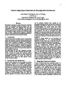
FTL Design Exploration in Reconfigurable High-Performance SSD for Server Applications Ji-Yong Shin†‡ Xiong-Fei Cai†
Zeng-Lin Xia† Ning-Yi Xu† Rui Gao† ‡ Seungryoul Maeng Feng-Hsiung Hsu†
†
‡
Hardware Computing Group Microsoft Research Asia Beijing, China, 100190 {zlxia, ningyixu, ruigao, xfcai, fhh} @microsoft.com
Korea Advanced Institute of Science and Technology Daejeon, Korea, 305-701 {jyshin, maeng} @camars.kaist.ac.kr
ABSTRACT
1. INTRODUCTION
Solid-state disks (SSDs) are becoming widely used in personal computers and are expected to replace a great portion of magnetic disks in servers and supercomputers. Although many high-speed SSDs are present in the market, both the design of hardware architecture and the details of the flash translation layer (FTL) are not well known. Meanwhile, in the systems requiring high-end storages, specially tuned SSDs can perform better than the generic ones, because the applications in such environment are usually fixed. Based on the architectural design of our reconfigurable high-performance SSD prototype and by using a trace-driven simulator, we explore the key factors and tradeoffs that must be considered when designing a customized FTL. FTL related issues, such as data allocation, cleaning, and wear leveling, are analyzed in detail presenting suitable design decisions for different workload characteristics. The experimental result shows that the figures for the performance metrics will vary from several percent to more than tens of times among each other depending on the decision made for designing each FTL functionality.
Recent advancement of NAND-flash based solid-state disks (SSD) is expected to impact greatly on the future of storage subsystems [7, 1]. The reason for this is SSDs provide superior features, such as higher performance and lower power consumption, compared to magnetic disks. However, to utilize SSDs a variety of design criteria must be considered. Specifically, design of the flash translation layer (FTL) must be carefully reviewed. Even with the same hardware organizations, the performance and the lifetime of each SSD can significantly differ depending on the FTL design. In addition, the performance of flash memory-based devices is highly workload sensitive [1], making the design decision for FTL more crucial. In the environments that require high-end storages, such as in servers and supercomputers, applications are likely to be fixed. Thus, FTL design for specific applications will leverage the performance of the system. However, to the best of our knowledge there hasn’t been any research publication focusing on the application specific FTL design in SSDs for high-performance environment. In this paper, we analyze the key factors and tradeoffs for customizing FTL regarding workload characteristics in a high performance SSD (HPSSD) environment, and propose guidelines for FTL design decisions. Efforts have made to utilize NAND flash memories in areas requiring high performance storages. The overall bandwidth of generic SSDs in the market is usually bounded by the host-to-SSD interface, such as SCSI, PATA, and SATA. Thus, multiple chips in the SSDs will usually share a flash channel, or a bus connecting flash chips and flash controller, and the channels will collectively have similar bandwidth to the interface. However, high-end SSDs for enterprise servers [8] take advantage of a host-to-SSD interface with gigabytes of bandwidth. Acceleration platforms using NAND flash chips [27, 18], employ independent channels per flash chips to gain maximum parallelism. Accordingly, we define the HPSSD as SSDs with high-bandwidth host-to-SSD interface as large as several gigabytes per second and tens or hundreds of flash chips and channels that can be parallelized to fully utilize the interface. Yet, in research using the acceleration platforms, very generic FTLs are used, and for most of the SSDs in the market the designs of FTLs are kept as the manufacturers’ intellectual properties.
Categories and Subject Descriptors B.1.4 [Microprogram Design Aids]: Firmware engineering; B.3.3 [Performance Analysis and Design Aids]: Simulation
General Terms Design, Measurement and Performance
Keywords NAND flash memory, FTL design, solid state disk, high performance SSD
Permission to make digital or hard copies of all or part of this work for personal or classroom use is granted without fee provided that copies are not made or distributed for profit or commercial advantage and that copies bear this notice and the full citation on the first page. To copy otherwise, to republish, to post on servers or to redistribute to lists, requires prior specific permission and/or a fee. ICS’09, June 8–12, 2009, Yorktown Heights, New York, USA. Copyright 2009 ACM 978-1-60558-498-0/09/06 ...$5.00.
338
Operation Page read to register Page write from register Block erase Page register access through flash channel
Table 1: Timing parameters for NAND flash chips chips in Table 1. SLC chips are used to take advantage of the high performance and endurance in IO intensive environments.
2.2
NAND Flash Chip Organization and Operations )ODVK�&KLS
3ODQH
3ODQH
Characteristics of NAND Flash Memory
���
3ODQH
3DJH
���
3ODQH
%ORFN 3DJH
'LH
%ORFN 3DJH 3DJH 3DJH�5HJLVWHU &DFKH�5HJLVWHU
Figure 1: Flash chip organization The capacities of flash chips used in this paper are 4GB and 8GB. Although they share the same latencies for the basic operations, the internal organizations of the chips are different. Figure 1 shows the general organization of a flash chip. A NAND flash chip consists of dies which contains several planes. Within a die planes can be interleaved only when the same types of commands are issued together. A die is an independent unit that has its own ready/busy and chip-enable signals. The dies in a chip can execute different operations from each other in an interleaved manner. The difference between the two chips is that the 4GB chip consists of 2 dies while the 8GB chip consists of 4 dies. The rest of the organizational settings used in this paper are summarized in Table 2. For most of NAND flash chips interleaved plane and die commands, and read and write for copy commands are supported. The interleaved commands provide parallelism within a chip, and the read and write for copy commands enable a page to be copied within a plane without utilizing the flash channel. Page size Pages per block Blocks per plane Planes per die Dies per chip
NAND Flash memory consists of multiple blocks which are composed of pages. Flash blocks must be erased before data is written and the blocks wear out as they are being erased. The unit of read and write operations is a page while that of erase is a block, with the latencies for each operation differing depending on the manufacturer. There are two types of NAND flash memories: single level cell (SLC) and multi level cell (MLC). The capacity of MLC doubles that of SLC, but SLC has lower operational latency and higher endurance. The erase count that a block in SLC can endure is typically 100K, while it is 10K in MLC. In this paper, we used a configuration of SLC NAND flash
3ODQH
'LH
2. BACKGROUND AND RELATED WORK 2.1
Time required 25 μs 250 μs 500 μs 100 μs
���
Previous research has focused mostly on FTLs in limited resource environments, such as embedded devices or low cost SSDs. In particular, considering the limited size of random access memory (RAM), the focus has been on log-based block mapping algorithms [20, 21, 14, 24]. Because highoverhead block merge operations are involved, they perform worse than page mapping algorithms. In addition, bandwidth to SSD is often limited, so only a few flash chips on shared channels are employed [1, 17]. Thus, not many ways to manage wear level and to maximize parallelism among a large number of independent chips as in HPSSDs are studied. Throughout our work we have discovered some tradeoffs in designing FTLs for HPSSDs. The experimental results show that, different from the embedded flash storage environments utilizing few flash chips, tradeoff lies between gaining high performance and reducing the number of erase operations for longer lifetime of SSDs. Introducing wide striping-based allocation in unit of page or greedy-based dynamic methods may maximize parallelism, but high locality of write, which reduces the number of erase operations, can be achieved when large striping units than a page size are used for allocations. By introducing a novel concept of wear leveling cluster we also have verified the tradeoffs between achieving even wear level in a large area and gaining high performance. Considering the workload characteristics, sequential IO intensive workloads benefits from wide striping based allocation methods, while random IO intensive workloads run better on dynamic based allocations. When the data and requests are distributed evenly within a SSD, hot/cold data separation can help reduce the cleaning overhead. When data are skewed, however, proposed load balancing can resolve the situation with low overhead. The experimental results collectively show that the workload characteristics and the corresponding design decisions for each FTL functionality changes the figures of the performance metrics from several percent to more than thousands of percent. The rest of the paper is organized as follows. Background information about NAND flash memory, reconfigurable HPSSD (RHPSSD), which provides the base architecture for HPSSD in this paper, and related works will be introduced in Section 2. Section 3 will provide the exploration of design considerations in FTL. Section 4 will present the evaluation work regarding the discussions in the previous section. Our study will be summarized in Section 5, and finally a conclusion will be given in Section 6.
4GB Chip 4KB 64 4096 2 2
8GB Chip 4KB 64 4096 2 4
Table 2: Internal organizational settings of NAND flash chips Open NAND flash interface (ONFI) 2.0 [23] compliant flash chips provide cache mode operations using cache registers. If each plane has only one page register, flash channel operation and plane access operation cannot be pipelined, because the page register must be exclusively available to the either operation. However, introducing the cache register
339
important, because each module contributes to the parallel performance. Although the RHPSSD might not be the standard design for HPSSDs, we expect that most HPSSDs will have similar high level organizations.
and the cache mode commands enables the both operations to be executed independently.
2.3
Role of FTL
The primary role of FTL is to provide abstraction of the flash memory characteristics to the host machine: maintaining an address mapping table, cleaning the blocks for reuse, and conducting wear leveling are some of the basic functions. As employing multiple NAND flash chips as in SSDs becomes common, FTL should also consider the parallelism and the load balancing of requests among flash modules such as chips, dies, and planes.
2.4
2.5
Agrawal et al. [1] have studied the tradeoffs that lie in SSDs focusing on the different organization of flash chip arrays and corresponding basic FTL issues. However, we fix the SSD architecture to the extreme to gain the highest performance, and concentrate on the detailed analysis and tradeoffs in each FTL functionality considering the workload characteristics. Park et al. [24] proposed a dynamically reconfigurable FTL in a block mapping scheme, but the focus of the work was reducing the number of erase operations using different block mapping algorithms without considering the multichip environments. In this paper, page mapping is used, FTL related issues in multi-chip environments are covered more comprehensively, and concerns of statically reconfiguring FTL are studied. Data allocation to multiple chips in SSDs are very similar to the issues studied in the RAID [25] system. The adaptive striping method for a flash chip with banks, or dies employing one plane each, has been investgated by Chang and Kuo [4]. Different from our paper the investigation involved only one chip with multiple banks and posed passive measures to deal with load imbalance among banks. There were also approaches to optimize the array of disks in accordance with workload characteristics, such as in HP AutoRAID [31] and by using RAID configuration tools [33]. Yet, SSDs do not have moving mechanical parts, and cleaning and wear leveling operations distinguishes the factors that must be considered.
Reconfigurable High Performance SSD
The discussion about the FTL design in the rest of the paper will be based on the architecture of the RHPSSD prototype that we have designed and are currently testing. In our RHPSSD, PCI Express is used as the host-to-SSD interface. A total of 4GB/s uplink and downlink provides sufficient bandwidth to fully utilize tens of flash chips in parallel. The high level view of the SSD prototype is shown in Figure 2. The SSD has a FPGA between the PCI Express bus and the flash channels. The FPGA is where the FTL and the flash channel controllers are implemented. FTL can be implemented and utilized as software by adding a general purpose processor on the FPGA or as hardware by using HDL code. This flexibility makes our prototype reconfigurable and facilitates the FTL to be customized. The flash-channel controllers are independently implemented in FPGA for each channel to maximize parallelism. Each flash chip possesses an independent flash channel and is placed on a daughter board that can be disconnected from the main board of the RHPSSD. There are more than 30 flash chips on the daughter board and the bandwidth between the daughter and the main board is sufficient enough to utilize all the flash channels at the same time. RHPSSD also has a large amount of RAM that can be utilized by the FTL. Although the RAM can be used as cache buffers, we leave using it as the buffer for future work.
3. EXPLORATION OF DESIGN CONSIDERATIONS FOR SPECIALIZED FTL 3.1
Daughter Board Flash chip
Flash chip
Flash chip
Flash chip
Flash chip
Flash chip
Flash chip
Flash chip
Flash chip
Flash CH Ctlr Flash CH Ctlr
Flash chip
Flash chip
...
...
... Flash CH Ctlr
...
Flash CH Ctlr
FTL
Page Mapping Algorithms
Taking advantage of abundant RAM in the RHPSSD architecture, we focus on page mapping methods. Logical pages in flash memories are not stored in a fixed position. A Concept of allocation pool is used to limit the assignable physical locations of logical pages to physical flash modules. Within the allocation pools logical pages are assigned to physical pages in runtime. Depending on the size of the allocation pool and the allocation policy the performance of SSD can vary. Because a plane is the smallest unit that can process a page request, we set the minimum allocation pool as plane and the maximum as SSD in this paper. Thus, we define allocating page addresses statically to planes as static allocation and using larger allocation pools as dynamic allocation since a logical page can be allocated to any plane within the pool in runtime.
Random Access Memories
FPGA
Related Work
Flash chip
PCI EXPRESS
Figure 2: High-level view of reconfigurable highperformance SSD
3.1.1
Compared to the generic SSDs the performance of RHPSSD will be greatly affected by the algorithms used to keep the chips busy. Wear leveling is considered more important than in the generic ones, because RHPSSD is likely to be placed under IO intensive environments. Additionally, maintaining even wear level among flash modules is
Static Allocation
Utilizing a static allocation can be very convenient if the allocation can distribute the requests evenly to each plane, because flash modules will be automatically parallelized and the wear levels among the modules will be balanced. However, an improperly skewed distribution of requests to few
340
However, most methods for identifying data’s hotness or coldness are on the basis of history based prediction. They work well with most cases, but depending on the workload characteristics or the allocation policies the prediction may lead to misclassification of data, further degrading the cleaning performance.
flash modules can rather degrade the overall performance. Organization and properties of flash chips, and workload characteristics must be considered before determining how to allocate the addresses. Taking these into account, there can be a variety of striping-based allocation methods. Although the plane is the unit that will be in charge of processing each stripe, striping the addresses to planes can be carried out in different sequences presenting different performances. Striping the address in a fine grain manner to gain parallelism may seem to result in good performance, but considering the wear leveling and cleaning operation the choice may not always be optimal. A small striping unit may not benefit from spatial locality within blocks and result in more valid page migrations during cleaning operations. This can again do harm to the lifetime of SSD because increased page migrations causes more erase operations.
3.1.2
3.3
Dynamic Allocation
As studied earlier in the RAID systems, workloads with small and random IO access patterns will not benefit much from using static striping-based allocation, because small requests cannot usually take advantage of parallel operations and the requests may be skewed to a small number of disks [22, 11, 9]. Dynamically allocating the requests to storages can be a potential solution, but again the amount of data in each storage location can be imbalanced. For example, if write requests are skewed to only a few storage devices, the devices will be full and no longer capable of receiving new data. Then the storage system will lose parallelism and from a SSD point of view the wear leveling will also be harmed. One of the easiest ways to avoid the load imbalance in dynamic allocations is migrating data to storage devices with relatively more free space [28]. For SSDs migrating cold pages to the flash module with a small number of valid pages will balance the number of hot and cold data in each flash module and will likely benefit the wear leveling at the same time. Considering planes as disks the flash modules in an allocation pool can be considered as an IO system in charge of distributing the request dynamically to planes. When the allocation pool is set to a large unit it will have more flexibility to assign the requests, but unless a larger degree of freedom is managed in a very intelligent way high performance will not always be guaranteed.
3.2
Wear leveling
Wear leveling and cleaning operations cannot be separated from each other, because cleaning will wear out the blocks. Consequently, wear leveling algorithms are commonly triggered during cleaning or write operations [16, 5, 3]. There have also been studies on triggering wear leveling algorithms periodically [32], but it is not desirable to use periodic measures in environments, where it is difficult to predict when the flash modules will be idle. Following Pareto’s 80/20 rule, there are usually blocks of data that have rare access frequencies. Wear leveling usually involves migrating this data to the blocks with less remaining lifetime. Because migrating a block of pages requires tens of reads and writes, it can degrade the IO response time. Here we introduce a concept of wear leveling cluster. The cluster is similar to the allocation pool. The wear leveling algorithms will balance the lifetime of blocks only within the same cluster. Thus, the remaining lifetime of blocks from different cluster can have large gaps. When the cluster is large, the lifetime of blocks will be distributed evenly in SSD, but the maintenance overhead can be larger than using smaller cluster. The wear leveling cluster must be smaller than or equal to the allocation pool, because logical pages cannot be moved to the outside of the allocation pool. Therefore, when static allocations are used, the wear level of different flash modules can vary greatly, so selecting the static allocation with an even distribution of erase operations is necessary. In contrast, the size of the cluster can be selected for dynamic allocations depending on the size of allocation pool. The performance and wear leveling goal of the SSD must be considered to determine the size of the cluster.
4.
IMPLEMENTATION AND EVALUATION
In this section simulation-based evaluation of the issues discussed in the previous section and a more detailed analysis of FTL matters will be presented.
4.1
Simulation Environment
Our simulation environment was built after extensive modification of the DiskSim [10] based SSD simulation plugin [26]. Cache mode operation, a module aging flash chips, and various FTL functionalities that are discussed in the following sections were added. The aging module carries out write requests similar to each workload’s IO pattern until the cleaning operation is triggered in all planes before simulation starts. This module enables us to simulate an aged SSD, where there are few clean blocks to write and requires cleaning operations to secure writable blocks. Although SSD without aging shows better performance, the aging configuration reflects a more realistic situation. The base FTL follows the design of [2]. Other fixed configurations besides the latencies in Table 1 are summarized in Table 3. The amount of over-provisioned region and cleaning thresholds were fixed because the effect of controlling the former was already studied [1], and the latter does not
Cleaning and Hot/Cold Data Separation
Because the erase operation is conducted in a unit of blocks, valid pages in a block to be erased must be moved to another location. Thus, an important consideration for cleaning operations is to minimize the operational latency by reducing the number of page migrations so as not to delay the IO requests. Selecting the block with the minimum number of valid pages for cleaning is one of the most commonly used cleaning policies. It would be the best if we can find blocks with no valid pages, but it is not always the case. However, separating hot and cold data can facilitate reducing the number of page migrations [6, 12, 19]: blocks with only hot pages are likely to be full of invalid pages in the near future, while blocks with only cold pages are likely to maintain the number of valid pages.
341
Postmark (22GB) IOzone (16GB) WebDC (234GB) Overall Read Write Overall Read Write Overall Read Write IOPS 126.944 105.581 21.363 102.058 45.129 56.928 331.085 190.934 140.152 Avg. inter arrival time (ms) 8.006 9.625 41.798 6.752 15.502 11.958 3.032 5.247 7.163 Total data requested∗ 27,682K 17,455K 10,227K 642,110K 414,512K 227,598K 382,528K 161,109K 221,419K ∗ Data request per millisecond 56.444 35.591 20.853 54.961 35.480 19.481 42.131 17.744 24.387 Avg. req size∗ 444.635 337.092 976.150 538.527 786.180 342.203 127.251 92.934 174.002 TPC-C (154GB) SQL (223GB) Exchange (478GB) Overall Read Write Overall Read Write Overall Read Write IOPS 3,635.196 2,348.523 1286.673 61.872 39.617 22.255 90.519 49.740 40.779 Avg. inter arrival time (ms) 0.275 0.426 0.777 20.904 32.295 58.117 11.056 20.110 24.542 Total data requested∗ 112,108K 41,483K 70,625K 37,939K 11,230K 26,709K 1,836K 835K 1,001K ∗ Data request per millisecond 59.647 22.071 37.576 12.388 3.667 8.721 2.039 0.927 1.112 Avg. req size∗ 16.408 9.398 29.204 200.221 92.560 391.876 22.525 18.638 27.268 ∗ in unit of number of 512B disk sectors
Table 4: Workload characteristics Parameter Over-provisioning Cleaning threshold Use of cache mode operation Use of read and write for copy operation Use of interleaved plane operation Use of interleaved die operation Flash chips per flash channel Number of flash channels and chips per SSD
Value 13% 5% true true true true 1 36
other workloads are mostly dominated by sequential IOs. Although not described in the table, the requests in IOzone shows a very high locality compared to others. The majority of the logical pages in IOzone are accessed more than 32 to 40 times while those in others are accessed less than 16 to 32 times. Flash Chip 0 Die 0 Die 1 P0 P1 P0 P1 0 4 8 12 1 5 9 13 2 6 10 14 3 7 11 15
Table 3: Fixed configurations of SSD in simulations affect the performance much when SSD is aged. For high performance, the special operations supported by the chip are used as default when they can be issued. The SSDs are configured to hold 36 chips with independent channels. Other varying configurations will be introduced in each of the following subsections.
4.2
(a)
No striping
Flash Chip 0 Die 0 Die 1 P0 P1 P0 P1 0 4 1 5 8 12 9 13 16 20 17 21 24 28 25 29
Workload Analysis
(c)
The disk traces of workloads used in the experiments are as follows: Postmark [15], IOzone [13], WebDC, TPC-C [30], SQL, and Exchange. Postmark, IOzone, TPC-C, and Exchange traces are the same ones used [1], which we received from the authors. Postmark and IOzone are IO-intensive file system benchmarks, where the traces were gathered by running the benchmarks on workstation-class PCs. TPCC is a database benchmark for comparing the performance of online transaction processing and Exchange is a workload collected from a Microsoft Exchange server. WebDC is taken from running a highly IO-concentrated algorithm used to classify massive data collected from the web. SQL was obtained by running SQLIOSim [29], a software simulating IO behavior of Microsoft SQL Server 2005. SQLIOSim was configured to simulate a server with over 200 users on a 40GB database. Some of the characteristics of the traces are summarized in Table 4. The amount of the minimum address spaces necessary for the workloads are shown next to their names. Depending on the address space required, we used the configuration of one 144GB SSD with 4GB chips, one 288GB SSD with 8GB chips, and two 288GB SSDs with 8GB chips. IO operations per second (IOPS) of each trace and the amount of data requested per millisecond show how much IO stress leans toward the storage. Postmark, IOzone, WebDC, and TPC-C show highly IO intensive behavior compared to SQL and Exchange. Considering the request size, TPC-C and Exchange are random workloads. SQL shows a similar proportion of random and sequential IO requests and the
Flash Chip 1 Die 0 Die 1 P0 P1 P0 P1 16 20 24 28 17 21 25 29 18 22 26 30 19 23 27 31
Flash Chip 1 Die 0 Die 1 P0 P1 P0 P1 2 6 3 7 10 14 11 15 18 22 19 23 26 30 27 31
Die-wise striping from SSD point of view
Flash Chip 0 Die 0 Die 1 P0 P1 P0 P1 0 1 2 3 4 5 6 7 8 9 10 11 12 13 14 15
Flash Chip 1 Die 0 Die 1 P0 P1 P0 P1 16 17 18 19 20 21 22 23 24 25 26 27 28 29 30 31
(e) Plane-wise striping within sequentially allocated chip Flash Chip 0 Die 0 Die 1 P0 P1 P0 P1 0 1 8 9 2 3 10 11 4 5 12 13 6 7 14 15
Flash Chip 0 Die 0 Die 1 P0 P1 P0 P1 0 1 2 3 8 9 10 11 16 17 18 19 24 25 26 27
(b)
Plane-wise striping from SSD point of view
Flash Chip 0 Die 0 Die 1 P0 P1 P0 P1 0 4 2 6 8 12 10 14 16 20 18 22 24 28 26 30
(d)
Flash Chip 1 Die 0 Die 1 P0 P1 P0 P1 4 5 6 7 12 13 14 15 20 21 22 23 28 29 30 31
Flash Chip 1 Die 0 Die 1 P0 P1 P0 P1 1 5 3 7 9 13 11 15 17 21 19 23 25 29 27 31
Chip-wise and then die-wise striping from SSD point of view
Flash Chip 0 Die 0 Die 1 P0 P1 P0 P1 0 2 1 3 4 6 5 7 8 10 9 11 12 14 13 15
Flash Chip 1 Die 0 Die 1 P0 P1 P0 P1 16 18 17 19 20 22 21 23 24 26 25 27 28 30 29 31
(f) Die-wise and then plane-wise striping within sequentially allocated chip
Flash Chip 1 Die 0 Die 1 P0 P1 P0 P1 16 17 24 25 18 19 26 27 20 21 28 29 22 23 30 31
(g) Plane-wise striping within sequentially allocated die
Figure 3: Striping-based static allocation methods
4.3 4.3.1
Different Allocation Methods Striping-Based Static Allocations
For each workload, we tested seven different static allocations described in Figure 3. All the methods are based on striping except for (a), which simply allocates logical page addresses sequentially to each plane. (b), (c), and (d) are striping the addresses from a viewpoint of SSD: (b) is striping addresses to each plane not considering the die or chip; (c) is striping to dies first and again to each plane; and (d) is striping to each chip first, then to dies and finally to planes.
342
�����
� ��� � ��� �
D�EORFN E�EORFN F�EORFN G�EORFN H�EORFN I�EORFN J�EORFN D�SDJH E�SDJH F�SDJH G�SDJH H�SDJH I�SDJH J�SDJH
����
�� �� �� �
D�EORFN E�EORFN F�EORFN G�EORFN H�EORFN I�EORFN J�EORFN D�SDJH E�SDJH F�SDJH G�SDJH H�SDJH I�SDJH J�SDJH
� � � � D�EORFN E�EORFN F�EORFN G�EORFN H�EORFN I�EORFN J�EORFN D�SDJH E�SDJH F�SDJH G�SDJH H�SDJH I�SDJH J�SDJH
�� �� � �
D�EORFN E�EORFN F�EORFN G�EORFN H�EORFN I�EORFN J�EORFN D�SDJH E�SDJH F�SDJH G�SDJH H�SDJH I�SDJH J�SDJH
����
�� �� �� � �
�� � D�EORFN E�EORFN F�EORFN G�EORFN H�EORFN I�EORFN J�EORFN D�SDJH E�SDJH F�SDJH G�SDJH H�SDJH I�SDJH J�SDJH
D�EORFN E�EORFN F�EORFN G�EORFN H�EORFN I�EORFN J�EORFN D�SDJH E�SDJH F�SDJH G�SDJH H�SDJH I�SDJH J�SDJH
�
1RQ�$JHG
$JHG
(DFK�