Full-motion video display. Portable Functions ..... Ultra Low Power System Design. Technology .... on VLSI Circuits),. [
Basics of Low Power Circuit and Logic Design
Anantha Chandrakasan Massachusetts Institute of Technology
High Performance Processors Microprocessor Power (source ISSCC)
Power (Watt)
30
20
10
0 75
Basics of Low Power Circuit and Logic Design
80
85 Year
90
© Anantha Chandrakasan 1997
95
2
Portable Devices Required Portable Functions
Battery (40+ lbs)
■
Radio transceiver
■
Modem
■
Voice I/O
■
Pen Input
■
Text/Graphics Processing
■
Text/Graphics display
■
Video decompression
■
Full-motion video display
How to get 8 hours of operation ??? Basics of Low Power Circuit and Logic Design
© Anantha Chandrakasan 1997
3
Nominal Capacity (Watt-hours / lb)
Battery Trends 50
Rechargable Lithium
40 Ni-Metal Hydride 30 20 Nickel-Cadmium 10 0
65
70
75
80 Year
85
90
95
(from Jon Eager, Gates Inc. , S. Watanabe, Sony Inc.) Basics of Low Power Circuit and Logic Design
© Anantha Chandrakasan 1997
4
Where Does Power Go in CMOS?
Dynamic or switching currents ➟ Charging and discharging parasitic capacitors
Short-circuit or direct-path currents ➟ Direct path between supply rails during switching
Leakage currents ➟ Reverse bias diode leakage ➟ Sub-threshold conduction
Static currents
Basics of Low Power Circuit and Logic Design
© Anantha Chandrakasan 1997
5
Dynamic Power of a CMOS Gate Vdd E0->1 = CLVdd2
A1 AN
PMOS NETWORK
isupply
Vout NMOS NETWORK
CL
Vdd T T E 0 → 1 = ∫ P ( t )dt = V dd ∫ i supply ( t )dt = V dd ∫ C L dV out = C L • V dd 2 0 0 0 T T Vdd 1 2 E cap = ∫ P cap ( t )dt = ∫ V out i cap ( t )dt = ∫ C L V out dV out = --- C • V dd 2 L 0 0 0
Basics of Low Power Circuit and Logic Design
© Anantha Chandrakasan 1997
6
Modification for Circuits with Reduced Swing Vdd Vdd Vdd -Vt CL
E 0 → 1 = C L • V dd • ( V dd – V t )
Can exploit reduced swing to lower power (e.g., reduced bit-line swing in memory) Basics of Low Power Circuit and Logic Design
© Anantha Chandrakasan 1997
7
Physical Capacitance of an Inverter
Capacitance, fF
50.0
Cjunction + Cgate
40.0
30.0
Cjunction
20.0
Cgate
10.0
0.0 0.8
1.0
1.2
1.4
1.6
1.8
2.0
VDD
Important to account for capacitive non-linearities in power estimation Basics of Low Power Circuit and Logic Design
© Anantha Chandrakasan 1997
8
Node Capacitance is a Function of Voltage
Switched Capacitance, fF
110 100
LCLR
90 80 TSPCR 70
C2MOS
60 50 0.8
0.9
1.0
1.1
1.2
1.3
1.4
1.5
VDD, V
Basics of Low Power Circuit and Logic Design
© Anantha Chandrakasan 1997
9
Node Transition Activity and Power Consider switching a CMOS gate for N clock cycles E N = C L • V dd 2 • n ( N ) EN : the energy consumed for N clock cycles n(N): the number of 0->1 transition in N clock cycles EN 2 n(N ) P avg = lim -------- • f clk = lim ------------- • C • V dd • f clk N → ∞ N N→∞ N L α0 → 1 =
n(N ) lim ------------N→∞ N
P avg = α 0 → 1 • C • V dd 2 • f clk L
Basics of Low Power Circuit and Logic Design
© Anantha Chandrakasan 1997
10
Factors Affecting Transition Activity, α0->1 “Static” component (does not account for timing) ➟ Type of Logic Function (NOR vs. XOR) ➟ Type of Logic Style (Static vs. Dynamic) ➟ Signal Statistics ➟ Inter-signal Correlations
“Dynamic” or timing dependent component ➟ Circuit Topology ➟ Signal Statistics and Correlations
Basics of Low Power Circuit and Logic Design
© Anantha Chandrakasan 1997
11
Type of Logic Function: NOR vs. XOR Example: Static 2 Input NOR Gate
A
B
Out
0
0
1
0
1
0
1
0
0
1
1
0
Assume: p(A=1) = 1/2 p(B=1) = 1/2 Then: p(Out=1) = 1/4 p(0→1) = p(Out=0).p(Out=1) = 3/4 × 1/4 = 3/16
Truth Table of a 2 input NOR gate
α0->1 = 3/16
Basics of Low Power Circuit and Logic Design
© Anantha Chandrakasan 1997
12
Type of Logic Function: NOR vs. XOR Example: Static 2 Input XOR Gate
A
B
Out
0
0
0
0
1
1
1
0
1
1
1
0
Assume: p(A=1) = 1/2 p(B=1) = 1/2 Then: p(Out=1) = 1/2 p(0→1) = p(Out=0).p(Out=1) = 1/2 × 1/2 = 1/4
Truth Table of a 2 input XOR gate
α0->1 = 1/4
Basics of Low Power Circuit and Logic Design
© Anantha Chandrakasan 1997
13
Type of Logic Style: Static vs. Dynamic Vdd
Vdd A
CLK
B
A
A
B
B
CL
CL CLK
Power is only dissipated when Out=0! STATIC NOR
DYNAMIC NOR
α0->1 = 3/16
N0 3 α 0 → 1 = -------- = --N 4 2
Basics of Low Power Circuit and Logic Design
© Anantha Chandrakasan 1997
14
Another Logic Style: Dynamic DCVSL Vdd
Vdd
OUTB
OUT
I
IN INB I
Guaranteed transition for every operation! α0->1 = 1
Basics of Low Power Circuit and Logic Design
© Anantha Chandrakasan 1997
15
Influence of Signal Statistics on α0->1
B 0.2 2 P0->1 0.1 .1
p0->1
A
1 0.8 0.6 PB 0.4
0 0
A
B
CL
0
1
0.2 0.4 PA 0.6
pa
0.2 0.8
pb
0
10
1
p1 = (1-pa) (1-pb) p0->1 = p0 p1 = (1-(1-pa) (1-pb)) (1-pa) (1-pb)
α0->1 is a strong function of signal statistics Basics of Low Power Circuit and Logic Design
© Anantha Chandrakasan 1997
16
Inter-signal Correlations A
C
C
A Z
Z
B
B
(a) Logic circuit without reconvergent fanout
(b) Logic circuit with reconvergent fanout
p0->1 = (1- pa pb) pa pb = 3/16
pZ = p(C=1|B=1) • p(B=1) p0->1 = 0
Need to use conditional probabilities to model inter-signal correlations! CAD tools required for such analysis Basics of Low Power Circuit and Logic Design
© Anantha Chandrakasan 1997
17
“Dynamic” or Glitching Activity in CMOS
Cin
Add0
Add1
Sum Output Voltage, Volts
S0
Add2
Add14
S2
S14
S1
4.0
Add15 S15
4 S15
6 2.0
3
S10
Cin 5 S1
2
0.0 0
5
10
Time, ns
α0->1 can be > 1 due to glitching! Basics of Low Power Circuit and Logic Design
© Anantha Chandrakasan 1997
18
Glitch Reduction Using Balanced Paths F
A0 A1
A2
A3
A4
A5
A6
A7
Ripple A0 A1 A2 A3
F
A4 A5
Lookahead
A6 A7
Basics of Low Power Circuit and Logic Design
© Anantha Chandrakasan 1997
19
Comparison of Adder Topologies Power-Delay-Product-1 16 bit
32 bit
64 bit
Ripple Carry
3.09
0.81
0.27
Carry Lookahead
10.0
3.54
1.76
Carry Bypass
5.45
2.39
0.99
Carry Select
4.44
2.08
1.00
Conditional Sum
3.82
1.23
0.42
Logic Transition Histogram
from [Callaway92] (VLSI Signal Processing, V)
Basics of Low Power Circuit and Logic Design
© Anantha Chandrakasan 1997
20
Glitching at the Datapath Level A B C
A
+
D
B
+
+
C
+
+
Tree vs. Chain
D
+
(A + B) + (C + D)
(A + B) + C + D
Inputs Normalized # of Transitions Tree
Chain
4
1
1.45
8
1
2.5
Can be reduced by reducing the logic depth and balancing signal paths Basics of Low Power Circuit and Logic Design
© Anantha Chandrakasan 1997
21
Short-circuit Component of Power Vdd
Vin
Vout CL
IVDD (mA)
0.15
0.10
0.05
0.0
1.0
2.0 3.0 Vin (V)
Basics of Low Power Circuit and Logic Design
4.0
5.0
© Anantha Chandrakasan 1997
22
Short-Circuit Current vs. Load Capacitance
from [Veendrick84] (IEEE Journal of Solid-State Circuits, August 1984)
Basics of Low Power Circuit and Logic Design
© Anantha Chandrakasan 1997
23
Minimizing Short-circuit Power 0.5
∆E / E(tRin=0)
0.4 0.3
Device Sizes: W/LP = 7.2µm/1.2µm W/LN = 2.4µm/1.2µm Vdd = 5V
0.2 0.1 0.0 0.0
Vdd = 3V 0.5
1.0 tRin/tRout
1.5
2.0
Keep the input and output rise/fall times the same (< 10% of Total Consumption) from [Veendrick84] (IEEE Journal of Solid-State Circuits, August 1984)
If Vdd < Vtn + |Vtp| then short-circuit power can be eliminated! Basics of Low Power Circuit and Logic Design
© Anantha Chandrakasan 1997
24
Reverse Biased Diode Leakage GATE
p+
+
p
N Reverse Leakage Current +
V - dd
IDL = JS × A JS = 1-5pA/µm2 for a 1.2µm CMOS technology Js double with every 9oC increase in temperature Basics of Low Power Circuit and Logic Design
© Anantha Chandrakasan 1997
25
Subthreshold Leakage Component 10-2 10-3 10-4 10-5
ID, A
10-6
VT = 0.1V
VDS=1V ID
VT = 0.4 V
10-7 10-8
VGS +-
10-9 10-10 10-11 10-12
0
0.1
0.2
0.3
0.4
0.5
0.6
0.7
0.8
0.9
1.0
VGS, V
Leakage control is critical for low-voltage operation Basics of Low Power Circuit and Logic Design
© Anantha Chandrakasan 1997
26
Static Power Vdd
Istat Vout
Vin=5V
CL
Pstatic = p(In=1).Vdd . Istat
• Not a function of switching frequency
Basics of Low Power Circuit and Logic Design
© Anantha Chandrakasan 1997
27
Ultra Low Power System Design System
Design partitioning, Power Down
Algorithm
Complexity, Concurrency, Locality, Regularity, Data representation
Architecture
Concurrency, Instruction set selection, Signal correlations, Data Representation
Circuit/Logic
Transistor Sizing, Logic optimization, Activity Driven Power Down, low-swing logic, adiabatic switching
Technology
Threshold Reduction, Advanced packaging
Lower Supply Voltage and Switched Capacitance Basics of Low Power Circuit and Logic Design
© Anantha Chandrakasan 1997
28
Signal Processing Attributes Throughput constrained computing - 30ms refresh rate requirement for video - Optimize power supply voltages
Time-varying computational requirements - Adaptive signal processing techniques
4000
Speech Data
“water all year” 2000
0
-2000
-4000
Time Basics of Low Power Circuit and Logic Design
Transition Probability
Knowledge of signal statistics 0.7 0.6
Sign-extension
0.5 0.4 0.3 0.2 0.1 0.0
0
5
10
15
Bit Number © Anantha Chandrakasan 1997
29
Energy Efficiency Metric: Fixed Throughput Example: Video Compression
P = (Σ (NiCiVdd2)) fsample Energy/Sample
fsample is fixed For this mode (most DSP applications), minimizing energy/sample is both Energy and Power Efficient
Basics of Low Power Circuit and Logic Design
© Anantha Chandrakasan 1997
30
Energy Efficiency Metric: Max Throughput Process Queue
from [Burd95] (HICSS 95)
Energy/operation Power ETR ≡ ------------------------------------- = ------------------------------------2Throughput Throughput A lower ETR (higher efficiency) indicates lower energy for constant throughput, or higher throughput for constant energy
Other metrics such as E x D, see [Horowitz94], (1994 Symposium on Low-power Electronics) Basics of Low Power Circuit and Logic Design
© Anantha Chandrakasan 1997
31
NORMALIZED DELAY
Supply Voltage Scaling 7.5 7.0 6.5 6.0 5.5 5.0 4.5 4.0 3.5 3.0 2.5 2.0 1.5 1.0
multiplier
2.0µm technology
clock generator
Td =
CL • Vdd I
I ~ (Vdd - Vt)2 ring oscillator
Td(Vdd=1.5)
microcoded DSP chip
Td(Vdd=5)
adder adder (SPICE) 2.0
4.0
=
(1.5) • (5 - 0.7)2 (5) • (1.5 - 0.7)2
≈ 8 6.0
Vdd (volts)
Lowering Vdd reduces energy but increases delays Basics of Low Power Circuit and Logic Design
© Anantha Chandrakasan 1997
32
Technology Based Voltage Scaling
Vdd
Vout
VDSAT
Vout CL
0.9Vdd
0.1Vdd
Fall Time: τ
Vin
Vin τ2
τ= ∝
τ1 +
V τ1∼ const. dd -1
τ2
time
from [Kakumu90] (IEEE Tran. on Electron Devices)
Power Supply Voltage: V dd(V)
Exploit velocity saturated sub-micron devices to lower voltage without significant loss in device speed Technology based “Optimal” Vdd: 2.43V for 0.3µm CMOS Basics of Low Power Circuit and Logic Design
© Anantha Chandrakasan 1997
33
Supply Voltage Scaling Using VT Reduction 1.5 1.25
VDD,V
1.0
tpd=645pS
tpd=420pS
0.75
tpd=840pS
0.5 0.25 0.0 0.05
0.15
0.25
0.35
0.45
VT, V
Threshold voltage reduction enables voltage scaling without performance loss Basics of Low Power Circuit and Logic Design
© Anantha Chandrakasan 1997
34
Optimizing Continuous Mode Circuits 1.25
tpd=420pS Energy (pJ)
1.00
VDD=1.02V
VDD=1.4V
0.75
VDD=0.55V 0.50
VDD=1V VDD=0.67V
VDD=0.34V
tpd=840pS
0.25 0.0 0.05
0.15
0.25 VT (V)
0.35
0.45
Optimum VDD/VT point trades-off switching and leakage power and is a strong function of activity also see [Burr94] Basics of Low Power Circuit and Logic Design
© Anantha Chandrakasan 1997
35
Limits of Supply Voltage Scaling CMOS Inverter Transfer Curves Vout
0.7 0.6
Output Voltage (V)
0.6
0.5
0.5
0.4
0.4
Experiment
0.3
0.3 0.2
0.7 V = Vs
Calculation
0.2 0.15
0.1 0.1 0
0.2
0.2
0.3
0.4
0.5
Input Voltage (V)
0.6
0.7 Vin
Vsmin ≥ 2-4 kT / q from [Swanson72] (IEEE JSSC, April 1972) Basics of Low Power Circuit and Logic Design
© Anantha Chandrakasan 1997
36
Burst Mode or “Event Driven”Computation BLOCKED (waiting for hardware events and client requests)
RUNNING (doing actual computation) Trunning
Tblocked
“On”
“Off”
Trace Length (sec) Toff (sec) Ton (sec) Toff/(Toff+Ton)
Trace 1
Trace 2
5182.48 5047.47 135.01 0.9739
26859.9 26427.4 432.5 0.9839
Trace 3 995.16 960.82 34.34 0.9655
For an X-server application, processor spends most of the time in the blocked or off state. from [Srivastava95] (IEEE Trans. on VLSI Systems) Basics of Low Power Circuit and Logic Design
© Anantha Chandrakasan 1997
37
Techniques for Burst Mode Computation SLEEP
High VT
Multiple VT Technology
Low VT
(Disable high VT devices during idle periods) e.g., [Sakata93] (Symposium on VLSI Circuits), [Mutoh93] (International ASIC Conference)
SLEEP
High VT
High VT transistor sizing issues Preserving state requires extra transistors Basics of Low Power Circuit and Logic Design
© Anantha Chandrakasan 1997
38
Latch Design in MTCMOS
SLEEP
SLEEP
High VT
High VT
SLEEP
High VT
SLEEP
High VT
CLK
From S. Mutoh, et. al. JSSC, August 1995 Basics of Low Power Circuit and Logic Design
© Anantha Chandrakasan 1997
39
Techniques for Burst Mode Computation VDD + VP > 0
ON
standby
Vout
Vin
Substrate Bias Controlled Variable VT Devices (Increase VT during idle periods)
standby ON
from [Seta95] (ISSCC 1995)
+ - VN < 0
Needs large body factors - large well capacitances Triple well process needed
Basics of Low Power Circuit and Logic Design
© Anantha Chandrakasan 1997
40
SOI with Active Substrate (SOIAS) tfox
n+
p
n+
p+
Loverlap
SiO2 p+
i-poly
tsi
n
tbox
p+ SiO2
n+
SiO2
Silicon Substrate
Backgate Control Enables Dynamically Varying Threshold Voltages from [Yang95] Basics of Low Power Circuit and Logic Design
© Anantha Chandrakasan 1997
41
NMOS Device Characteristics Vt=0.448 V (Vgb=0.0 V) Vt=0.184 V (Vgb=3 V)
-2
10
10-3
0.03
10-4
1.8x
10-6 10
10-8
0.02
Leff=0.44 um tsi=4.5 nm tfox=9 nm tbox=100 nm VDS=1.0 V
-7
~ 4 Dec
10-9 10-10
Id (mA/um)
Id (mA/um)
10-5
0.01
10-11 10-12 10-13 0 -0.2
0
0.2
0.4
0.6
0.8
1
Vgf (V) Basics of Low Power Circuit and Logic Design
© Anantha Chandrakasan 1997
42
Ring Oscillator Frequency (MHz)
Ring Oscillator Characteristics 12 Varied VTN only VTP= - 0.2V 10
8
6 0.0
Varied VTP only VTN = 0.512V
0.1 0.2 0.3 0.4 0.5 0.6 0.7 Backgate Controlled Variable |V T| (V)
Processor speed is adjustable on demand
Basics of Low Power Circuit and Logic Design
© Anantha Chandrakasan 1997
43
Architectural Model & Activity Parameters for SOIAS Add15
Add1 Circuit Node Transition Activity
a b
x
αx
0.4 4 P0->1 0.2 .2
1 0.8
0
0.2 0.4 PA 0.6
pa CLK ADD
CLK ADD
CLK BACKGATE
1
0.6 PB 0.4
0 0
0.2 0.8
pb
10 10
ADD OFF
ADD ON
ADD ON
fga = Module Activity Factor CLK BACKGATE
LOW VT
HIGH VT
LOW VT
bga = Backgate Switching Activity Basics of Low Power Circuit and Logic Design
© Anantha Chandrakasan 1997
44
Generic Architecture Model for All Technologies
Leakage Control Mechanism (hence affecting bga)
Technology Multiple Threshold Technology Substrate Bias Control Silicon On Insulator Active Substrate
Switching the High VT devices ON/OFF Controlling the Substrate Voltages Switching the Backgate Voltage
Hierarchy of Profilers and Statistical Models Required for “Virtual Prototyping” Basics of Low Power Circuit and Logic Design
© Anantha Chandrakasan 1997
45
Energy Estimation Models for SOI and SOIAS fga = Module Activity Factor bga = Backgate Switching Activity α = Node Transition Activity Factor
ESOI = α fga CfgVdd2 + Ileak_lowVT Vdd Tcycle ESOIAS = α fga CfgVdd2 + fga Ileak_lowVT Vdd Tcycle + (1-fga)Ileak_highVT Vdd Tcycle + bgaCbgVbg2
Basics of Low Power Circuit and Logic Design
© Anantha Chandrakasan 1997
46
Architectural Profiling to Determine fga and bga Table 1. SPEC benchmark espresso Total Instructions Additions Shifts Multiplications
Number
fga
bga
900158847 543616709 57000715 172883
0.6039 0.0633 0.0002
0.1954 0.0541 0.0002
Number
fga
bga
1737729538 661236960 52224367 7088
0.6023 0.0087 0.0000
0.2233 0.0086 0.0000
Number
fga
bga
2125 1250 186 3
0.5882 0.0875 0.0014
0.2635 0.0753 0.0014
Table 2. SPEC benchmark Li Total Instructions Total Additions Total Shifts Multiplications
Table 3. Data Encryption (IDEA) Total Instructions Additions Shifts Multiplications
Basics of Low Power Circuit and Logic Design
© Anantha Chandrakasan 1997
47
SOI vs. SOIAS Technology Evaluation
Adder
0.5
Shifter
**
o
0.0 1
-0.5
−1 .
t-gate ac−2 −1.5 tivity fac t
−3.5 −1
or)
Basics of Low Power Circuit and Logic Design
−0.5
−4
ac
ga
log(fron
−3
−2.5
k-
−3
ac
−3.5
te
−2.5
(b
−4
−2
tiv
−2
ity
−1.5
fac
−1
)
-1.0
**
o
tor
0
log
log(ESOIAS/ESOI)
Mult. .
© Anantha Chandrakasan 1997
48
Transistor Sizing for Low-Power Higher Voltage
Lower Capacitance Small W/L’s
Large W/L’s Higher Capacitance
Lower Voltage
Larger sized devices are useful only when interconnect dominated Minimum sized devices are usually optimal for low-power
Basics of Low Power Circuit and Logic Design
© Anantha Chandrakasan 1997
49
Transistor Sizing for Fixed Throughput Cg = W/L CMIN
I ∝ W/L CMIN
CMIN = Minimum sized gate (W/L=1) W /L after sizing
CP = Cwiring + CDF
α = CP / (K CMIN)
HIGH PERFORMANCE W/L >> CP / (K CMIN)
LOW POWER W/L = 2 CP / (K CMIN) (if CP ≥ K CMIN) ELSE W/L = 1
NORMALIZED ENERGY
10 7
α=0
5 4 α = 0.5
3 2
α=1
1.5 adder
1.0 0.7
α = 1.5 α=2
0.5
from [Chandrakasan92] (IEEE JSSC, 1992) Basics of Low Power Circuit and Logic Design
1
3
10
W/L
© Anantha Chandrakasan 1997
50
Capacitance Breakdown MODULE LEVEL MODULE
GATE
DIFFUSION
INTERCONNECT
ADDER (Conventional Static)
30%
45%
25%
ADDER (Carry Select)
37%
31%
32%
TSPC COUNTER
32%
26%
36%
LOG SHIFTER (8 bit shift by 4)
15%
42%
43%
COMPARATOR
33%
38%
29%
DATAPATH LEVEL MODULE
GATE
DIFFUSION
INTERCONNECT
ADDER CHAIN ( 7 adders )
38%
38%
24%
WAVE DIGITAL FILTER
31%
29%
40%
ADDRESS GENERATION (STD CELL)
56%
24%
20%
VIDEO SYNC GENERATOR (STD CELL)
45%
25%
30%
Basics of Low Power Circuit and Logic Design
© Anantha Chandrakasan 1997
51
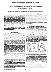
Choice of Logic Style B
VDD A A B B
A B
VDD
A
VDD
A B
A
A
B
A
C A
A
A
B
B
A
B
A
B
P
GEN
P
B
Sum
CIN
P
CIN
GND
B
A CC
CIN B
CIN
COSUM
B
B
B
B
CIN B
A
A
A
CIN A
B B
SUM
B
B
A
VDD PRE VDD A A
CO
P
OPTIMIZED static Adder B
VDD PRE VDD
COUT
GEN GND
CONVENTIONAL CMOS Adder
GEN
CIN
COUT CIN GEN
CIN
Cout
P PROP
P
C
GND VDD
VDD GEN
SUM
B
A B
CIN
A
GND
B
P
A
B
B
A
CIN
C B
B
A
B
A
B C
VDD
CIN
C C
A A
CIN A Sum
DCVSL Adder Basics of Low Power Circuit and Logic Design
Sum
Cout
Cout
CPL Adder © Anantha Chandrakasan 1997
52
Choice of Logic Style 200
POWER-DELAY PRODUCT (pJ)
150
8-bit adders in 2.0µm
Standard Cell
100 70 50 30 20
DCVSL
15 10
Optimized Static
7 5
Decreasing Vdd
CSA Conventional Static CPL - LOW Vt
3 10
30
100
DELAY (ns)
Power-delay product improves as voltage decreases. The “best” logic style minimizes power-delay for a given delay constraint. Basics of Low Power Circuit and Logic Design
© Anantha Chandrakasan 1997
53
Reducing the Energy/Operation at a Fixed Vdd
Heavily Loaded Bit-line
Vdd (=1.5V) M1 M2 ϕ o 6/2 3/9 o V(out) ϕ
M5
4/2
v(ϕ)
1.5
v(line)
0.5 0 0
20
40 60 t (ns)
80 100
Reduced Signal Swing Example: FIFO Memory
Power Reduction Over Rail-to-Rail Swing = Vdd/(Vdd-Vt)
Basics of Low Power Circuit and Logic Design
© Anantha Chandrakasan 1997
54
Reducing the Energy/Operation at a Fixed Vdd R
C
tr ADIABATIC CHARGING
E = (RC/tr)CV2
(for tr >> RC)
Applying slow input slopes reduces E below CV2 Useful for driving large capacitors (Buffers) Power reduction > 4 for pad drivers (1 MHz) ISI Basics of Low Power Circuit and Logic Design
© Anantha Chandrakasan 1997
55
Example: Stepwise Adiabatic Driver VN
N
V2
2
V1
1
RC charging steps
0
from [Svensson94]
CL
(IEEE Symposium on Low Power Design, 1994)
Vi = (i/N) V 2 1 --- • C L • V dd V dd V dd 2 E step = Q • V avg = C L • ----------- ⋅ ----------- = ---------------------------------N 2N 2 N 2 1 --- • C L • V dd E conventional 2 E total = N • ---------------------------------- = -----------------------------------------2 N N Basics of Low Power Circuit and Logic Design
© Anantha Chandrakasan 1997
56
Activity Driven Logic Level Power Down A[N-1] B[N-1]
MSB REG
MSB COMPARATOR A>B
CLK
A[N-2:0]
COMBINATIONAL REG
CLK
LOGIC
REG for bits 0->N-2
BLOCK MODIFIED REGISTER B[N-2:0]
REG for bits 0->N-2
COMPARATOR A>B for bits 0->N-2 CONDITIONALLY SWITCHED
GATED_CLK from [Alidina94] (1994 International Workshop on Low-power Design)
50% reduction possible for random inputs Basics of Low Power Circuit and Logic Design
© Anantha Chandrakasan 1997
57
Activity Reduction in Shift Registers N Length Shift Register
Data In
Data Out
fCLK
Pserial = NCreg V2 fclk N/2 Length Shift Register
Data In
Data Out
fCLK/2
Pparallel= 2 x (N/2 Creg V2 fclk/2) + Poverhead Basics of Low Power Circuit and Logic Design
© Anantha Chandrakasan 1997
58
Shift Register Power for Various Lengths
Normalized Power Dissipation
1.0 0.8 32-bit
0.6 0.4
64-bit 128-bit
0.2
256-bit
0.0 0
8
16 Degree of Parallelism
Basics of Low Power Circuit and Logic Design
24
© Anantha Chandrakasan 1997
32
59
Summary
• Power dissipation is a prime design constraint for portable systems • Low Power design requires optimization at all Levels • Sources of power dissipation have been analyzed • Technology, circuit, and logic design techniques have been described
Basics of Low Power Circuit and Logic Design
© Anantha Chandrakasan 1997
60
References [Alidina94] M. Alidina, J. Monteiro, S. Devadas, A. Ghosh, and M. Papaefthymiou, “Precomputation-Based Sequential Logic Optimization for Low Power,” 1994 International Workshop on Low-power Design, pp. 57-62, April 1994. [Burd95] T. Burd, R. Brodersen, “Energy Efficient CMOS Microprocessor Design,” Proceedings of the 28th Annual HICSS Conference, Vol. I, pp. 288-297 Jan. 1995. [Burr94] J. Burr, J. Shott, “A 200mV Self-Testing Encoder/Decoder using Stanford Ultra-low Power CMOS,” IEEE ISSCC, pp. 84-85, 1994. [Callaway92] T. Callaway and E. Swartzlander, Jr., “Optimizing Arithmetic Elements for Signal Processing,” VLSI Signal Processing V, pp. 91-100, IEEE Special Publications, 1992. [Chandrakasan92] A. P. Chandrakasan, S. Sheng, and R. W. Brodersen, “Low-power Digital CMOS Design,” IEEE Journal of Solid State Circuits, pp. 473-484, April 1992. [Horowitz94] M. Horowitz, T. Indermaur, R. Gonzalez, “Low-Power Digital Design,” Proceedings of the Symposium on Low Power Electronics, 1994. [Kakumu90] M. Kakumu and M Kinugawa, “Power-Supply Voltage Impact on Circuit Performance for Half and Lower Submicrometer CMOS LSI,” IEEE Transactions on Electron Devices, Vol 37, No. 8, pp. 1902-1908, August 1990. [Mutoh93] S. Mutoh, T. Douseki. Y. Matsuya, T. Aoki, and J. Yamada, “1-V High-speed Digital Circuit Technology with 0.5µm Multi Threshold CMOS,” IEEE Int. ASIC Conf., pp. 186-189, 1993. [Sakata93] T. Sakata, M. Horiguchi, K. Itoh, “Subthreshold-Current Reduction Circuits for Multi-GIGABIT DRAM’s,” 1993 Symposium on VLSI Circuits, pp. 45-46. [Seta95] K. Seta, H. Hara, T. Kuroda, M. Kakumu, T. Sakurai, “50% Active-Power Saving Without Speed Degradation Using Standby Power Reduction (SPR) Circuit,” IEEE ISSCC 95, pp. 318-319. [Srivastava95] M. Srivastava, A.P. Chandrakasan, R. Brodersen, “Predictive System Shutdown and Other Architectural Techniques for Energy Efficient Programmable Computation”, to appear in the IEEE Trans. on VLSI Systems, March 1996. [Svensson94] L.“J.” Svensson and J.G. Koller, “Driving a capacitive load without dissipating fCV2,” IEEE Symposium on Low Power Design, pp. 100–101, 1994. [Yang95] I. Yang, C. Vieri, A. P. Chandrakasan, D. Antoniadis, "Back Gated CMOS on SOIAS for Dynamic Threshold Control," 1995 IEEE International Electron Devices Meeting, December 1995. [Veendrick84] H.J.M. Veendrick, ‘‘Short-Circuit Dissipation of Static CMOS Circuitry and Its Impact on the Design of Buffer Circuits,’’ IEEE Journal of Solid-State Circuits, Vol. SC-19, pp. 468-473, August 1984.