implementation. Here we have used structural coding approach for the entire design. VHDL codes are written using. Xilinx ISE 10.1 version and synthesized it.
International Journal of Computer Applications (0975 – 8887) Volume 41– No.12, March 2012
Design and Implementation of a New Program Address Generator Unit in a DSP Processor KabirajSethi Dept of Electronics and Telecomm. Engg VSSUniversity of Technology, Burla-768018
ABSTRACT This paper presents the design and implementation of a new Program Address Generator (PAG) unit, which is a part of Program Control Unit (PCU) well suited for DSP Processors. This would be compatible with DSP56002 (DSP Processor from Motorola) at instruction level. The PAG provides hardware dedicated to support loops, which are frequent constructs in DSP algorithm. The proposed architecture of PAG has been modeled, verified and synthesized using VHDL description and synthesis tools. It is found that the proposed AGU generates actual address for program memory as per the given set of inputs. Simulation results are compared with the theoretical data and found correct.
General Terms VLSI design.
Key words VLSI implementation; Program Control Unit; Program Address Generator; VHDL; DSP Processor.
Rutuparna Panda Dept of Electronics and Telecomm. Engg VSS University of Technology, Burla-768018
DSP and a general purpose processor. Eric Tell has carried out the Thesis work on the design of a domain specific DSP processor [15]. The first part of the Thesis gives different steps of design process and motivates the design decision made for the processor. The second part of the Thesis discusses design specifications. The evolution of DSP processors has been discussed by J Eyre and J Bier [16]and they expected a continuing evolution of DSP processors as par with the changes in technology. Roland Waltersson [17] has described the implementation of a Program Address Generator in a DSP processor. Guda Krishna Kumar [18] developed the Behavioral Model of an Instruction Decoder of Motorola DSP56000 Processor. Design and Implementation of Single Issue DSP is presented in [18]. Vinodh Ravinath describes the design of control path in a DSP Processor [19]. S Powel et al. [20] have presented three optimization techniques to reduce the energy in the data path, memory system and the instruction cache data bus. J Edwin et al. [21] explained the various DSP architectures and implementations. They also discussed the state-of-the art and examine the issues pertaining to performance of DSP processors. All these techniques more or less emphasize either design of a single unit or design of complete DSP processor. This has motivated the authors to present a new approach for design of PAG.
1. INTRODUCTION The present work aims at design and simulation of a Program Address Generator (PAG) [1-6].From the literature [7-12], it is found that the main thrust has been to optimize speed, power and area of a DSP processor. The PCU is considered to be an important part of a DSP processor. Several researchers have investigated new design techniques for the design of PCU and related units. J Eyre and J Bier [13] have described utility of DSP processors in digital home audio, for down loading audio from internet and voice over internet. J Eyre [14] has presented a framework for understanding the DSP processor architecture including the interchange of architectural technique between a
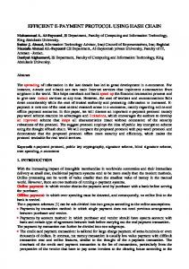
The Program Control Unit (PCU) is one of three execution units (i.e. Address Generation Unit, Data Arithmetic Logic Unit and Program Control Unit) on the DSP56002 core [2224] as shown in the Figure 1. It performs program address generation (instruction prefetch), instruction decoding, hardware do loop control, and exception (interrupt) processing. The PCU consists of three hardware blocks: the program decode controller (PDC), the program address generator (PAG), and the program interrupt controller (PIC).PAG controls the fetch stage of pipeline. It fetches the next instruction in program memory (PM) to be decoded.
29
International Journal of Computer Applications (0975 – 8887) Volume 41– No.12, March 2012
EXTERNAL ADDRESS BUS SWITCH
YAB ADDRESS GENERATION UNIT
XAB PAB
PROGRAM MEMORY
X DATA MEMORY
Y DATA MEMORY
BUS CONTROL
YDB INTERNAL DATA BUS SWITCH
EXTERNAL DATA BUS SWITCH
XDB PDB GDB PROGRAM CONTROL UNIT
DATA ARITHMETIC LOGIC UNIT
Fig 1: Block diagram of Motorola 56002 DSP in a HDL) into an optimized technology-specific gate level implementation. Here we have used structural coding We have chosen a DSP processor as an apparatus due to its approach for the entire design. VHDL codes are written using following advantages. Most DSP Processors are meant to Xilinx ISE 10.1 version and synthesized it. ModelSimXEhandle high performance, repetitive, numerical task like the III6.3c (starter version) is used for simulation to verify the famous multiply and accumulate (MAC) operation. Second functionality of the circuit, based on inputs provided. important feature in DSP Processors is the ability to handle SPARTAN-III FPGA (field programmable gate arrays) several memory accesses in the same instruction cycle like 3s400fg320-4is used as target device for implementation as it fetching instructions, while fetching operands or storing the provides the benefit of high integration levels and quick result of previous computations to memory. Third feature is verification. FPGA devices are software configured and field the ability to generate address using the address generation programmable. So there is significant cost savings in design section in parallel with the other instructions; though initially and productions. Timing simulation determines the the address generation has to configured and set. The DSP propagation delays that are expected in the implemented Processor has a loop counter implemented within, therefore circuit. Chip configuration configures the actual chip to there is no necessary for the programmer to expand the realize the designed circuit. instruction cycle to implement a for-next loop. Here the designed control unit is more straightforward and has faster data transfer, addressing, arithmetic operations and 3. INSTRUCTION SET algorithms. We have considered many of the usual design The complete range of instruction capabilities combined with issues as this work has started from an already existing the flexible addressing modes used in this processor provides design. For example, one of the first encountered activities is a powerful assembly language for implementing the DSP the design of an instruction set for the processor. Other design algorithms. considerations include choosing native data length, degree of Syntax of the instruction: The instruction syntax instruction set parallelism, number of memory accesses per organized into four columns opcode, operands, and two clock cycle, number of pipeline stages etc. parallel move fields as shown below in Figure 2. Opcode Operands XDB YDB 2. DESIGN METHOD MAC X0,Y0,A X:(R0)+,X0 Y:(R4)+,Y0 We choose VHDL for the total design as it has several Fig 2: Syntax of the instruction advantages over other languages of its rank. It supports the picture of a multi-level design with different blocks The opcode column indicates the data ALU (Arithmetic Logic connected with buses and signal; thus making programming Unit), AGU (Address Generation Unit), or PCU (Program more logical and easier to grasp. The code can be written in Control Unit) operation to be performed and must always be sequential statements, or as a state machine. Also, one can included in the source code. The operands column specifies simulate the design and discover bugs and flaws before the the operands to be used by the opcode. The XDB and YDB synthesis, saving a great amount of time. Synthesis is the columns specify optional data transfers over the XDB and /or translation of a high level design into a specified hardware. It YDB and the associated addressing modes. The address space translates a register transfer level model of hardware (written
30
International Journal of Computer Applications (0975 – 8887) Volume 41– No.12, March 2012 qualifiers (X:, Y:, and L:) indicate which address space is being referenced. Instruction format: The DSP56002 Processor's instruction consists of 24-bit words - an operation word and an optional effective address extension word as shown in Figure 3. Most instructions specify data movement on the XDB, YDB, and data ALU operations in the same operation word. The data bus movement field provides the operand reference type. An effective address extension 23 DATA MOVEMENT
0 OPCODE x x x x x x x x OPTIONAL EFFECTIVE ADDRESS EXTENSION
16
PAB
Fig 3: Instruction Format
CLK
LA
INTRS
LC
4. DESIGN APPROACH The instruction set is divided into defferent groups such as Arithmetic,Bitmanipulation,Move,Logical,Loop and Program Control. For each groupn of instruction,the 24 bit instruction word from the program memory expansion block or any backup instruction register is fed to the PDC subsection of PCU. According to the type of instruction PDC decodes each group of bits to enable the desired control signal(s).The PAG unit’s task is to fetch the next instruction in program memory (PM). Under normal circumstances, the program counter (PC) is incremented with one. In case of loop or program control instructions, PAGworks in other ways and these exceptions are signaled by the PDC when such an instruction have been decoded.The instructions which cause a change in the flow of the PAG (branch control) are listed below.
a. Loop instructions:
The DO and ENDDO
instructions.
b. Program control instructions:All
jump & conditional jump instructions, all subroutine jump & conditional subroutine jump instructions, the return from subroutine (RTS) & return from interrupt (RTI) instructions and the repeat (REP) instruction.
5. PAG ARCHITECTURE PCU consists of three hardware blocks: Program Decode Controller, Program Address Generator and Program Interrupt Controller. PAG contains program counter (PC), stack pointer (SP), system stack (SS), operating mode register (OMR), status register (SR), loop counter (LC) and loop address (LA) as shown in Figure 4.
32 × 15 STACK
SP
CONTROL OMR
word following the operation word provides an immediate data address or an absolute address if required. The opcode field of the operation word specifies the data ALU operation or the program control unit operation to be performed, and any additional operands required by the instruction.
PDB
PC
87
BUS
24
SR 24
24
GLOBAL DATA BUS
Fig 4: Program Address Generator The PAG provides hardware dedicated to support loops, which are frequent constructs in DSP algorithms. A DO instruction loads the LC register with the number of times the loop should be executed, loads the LA register with the address of the last instruction word in the loop (fetched during one loop pass), and asserts the loop flag in the SR. The DO instruction also supports nested loops by stacking the contents of the LA, LC, and SR prior to the execution of the instruction. Under control of the PAG, the address of the first instruction in the loop is also stacked so the loop can be repeated with no overhead. While the loop flag in the SR is asserted, the loop state machine (in the PDC) will compare the PC contents to the contents of the LA to determine if the last instruction word in the loop was fetched. If the last word was fetched, the LC contents are tested for one. If LC is not equal to one, then it is decremented, and the SS is read to update the PC with the address of the first instruction in the loop, effectively executing an automatic branch. If the LC is equal to one, then the LC, LA, and the loop flag in the SR are restored with the stack contents, while instruction fetches continue at the incremented PC value (LA + 1).The repeat (REP) instruction loads the LC with the number of times the next instruction is to be repeated. The instruction to be repeated is only fetched once, so throughput is increased by reducing external bus contention.
6. IMPLEMENTATION Figure 5 shows the internal blocks of proposed PAG. The functional detail of these blocks is given below:
6.1 Program flow control Program Flow Control (PFC) is a synchronous finite state machine controlled by the master clock and a number of control signals generated from PDC. Output of LA~PC comparator is also one of the inputs to PFC.PFC controls the flow of PAG by sending control signals to the other synchronous parts of PAG. When an instruction is decoded and the control signals from the PDC are sent to PFC, the PC already points to the next instruction due to the pipeline. In startup mode, the PFC is in its idle state. On application of the clock pulse, the PAG leads to different branches depending on
31
International Journal of Computer Applications (0975 – 8887) Volume 41– No.12, March 2012 the last instruction decoded. The branches are normal, jump, subroutine jump, return from subroutine and return from interrupt, do loop, end of loop, continue loop and repeat. PDB IR
6.6 Loop address register
PDC CONTROL & DATA
SS PFC
SSH
SSL
The LA is a 16-bit wide register where the address of the last instruction of a hardware loop is stored. This register is only used in hardware loops. When LA is loaded with a new value, LA is pre decremented with one to support two-word instructions. It is stacked in the upper portion of SS during hardware loops.
6.7 Loop counter register
LA-PC
The LC is a 16-bit register used for hardware loops(DOloops) and for the REP instruction. If zero is loaded into LC, the LC is set to $FFFF. The LC also contains a 16-bit backup register that is used for REP instruction. The LC is stacked in the lower portion of SS during hardware loops.
PC SR SP GDB STATUS FLAGS
stack error flag bit which indicates that a stack error has occurred. SP (bit-5) is the stack underflow flag bit which is set during stack underflow. If either SP (bit-4 or 5) is set, a critical error is sent to the Interrupt Controller. Usually, SP is increased before a stack push and decreased after a stack pull.
LA LC
Stack row selector
PAB
Fig.5: Block diagram of proposed PAG
6.2 Program counter The PC is 16-bit register contains the address of the next location to be fetched from program memory space. It can point to instructions, data operands or addresses of operands. This is increased with one, or overwritten from a number of sources, declared by the PFC. The PC is stacked in SSH during subroutine jumps and hardware loops.
6.3 Status register The SR is a 16 bit register which consists of mode register (MR)in the high-order eight bits and a condition code register (CCR) in the low-order eight bits. The MR defines the current system state of the processor and contains flags such as the loop flag (LF), interrupt level etc. Almost every part of the DSP may affect the MR flags. The CCR defines the current user state of the processor, and contains among others the overflow, carry and scaling flags. The CCR bits are directly affected by the ALU operations. Each bit of it may also be independently read or written through a multiplexer with onehot addressing mode. The SR is stacked in the SSL during subroutine jumps and hardware loops.
6.8 LA-PC comparator Output of LA-PC comparator unit signals PFC regarding the end of loop. When loop flag (LF) in the SR is set, PC and LA are examined. If PC does not equal LA, nothing happens. The condition PC equals to LA indicates that the last instruction of the loop is already reached. Then if LC is equals to one, end of loop is signaled to the PFC. If LC is greater than one, continue loop is signaled and a new iteration starts.
6.9 Backup instruction register The backup IR is a 16-bit register stores an instruction while PAG is currently executing a REP instruction. The PDC reads this register instead of the PDB on the next instruction. This temporarily removes the fetch stage of the pipeline, and thus increases the execution speed.
6.10 SP-decoder The SP-Decoder translates SP (bits 0-3) into a 15 bit one-hot row selector. For example, if SP (bits 0-3) is equals to 0011, the output of the SP-Decoder will be 0000000000000100. The functionality of PAG for loop and program control instructions is summarized below. Here, in all cases the data is found in Global Data Bus (GDB). The number indicates the instruction cycle number.
Normal Fetch (most instructions):
6.4 System stack The SS is a separate 15x32-bit internal memory divided into two16 bit data registers, SSH and SSL for both higher and lower 16-bits respectively. This block is mainly used for the temporary storage of all the program registers values except stack pointer. It has the main functions at the operation of loops, jumps. Its operation is totally related to other registers.
6.5 Stack pointer The 6-bit SP indicates the location of the top of the SS and the status of the SS. The SP register works as a 6-bit counter that addresses a 15-location stack with its four LSBs. SP (bits 0-3) points to the last location used on the SS. SP (bit-4) is the
1.
PC