E-mail: {henriko, weidongl, deborahc, larsw}@isy.liu.se. ABSTRACT. In this paper the design and implementation of an SRAM layout generator is presented.
Design and Implementation of an SRAM Layout Generator Henrik Ohlsson, Weidong Li, Deborah Capello, and Lars Wanhammar Department of Electrical Engineering, Linköping University, SE-581 83 Linköping, Sweden E-mail: {henriko, weidongl, deborahc, larsw}@isy.liu.se
ABSTRACT In this paper the design and implementation of an SRAM layout generator is presented. The generated memories are aimed at implementation of system on chips for DSP applications. The purpose with the generator is to increase the design efficiency and reduce the dependency on commercial memories. The generator is implemented in SKILL in order to be easily modified for more advanced processes. The current version use a standard 0.18 µm CMOS process.
1. Introduction Memories are used in most DSP applications and are important components in system on chips. These memories are often relatively small. The memories required in one system on chip implementation are of different sizes and with different wordlengths. Hence, several different memories are required in each system. To increase the design efficiency we have developed a memory generator that generates layouts of relatively small static memories. The generator aim to reduce our dependency on commercial memories. Increasing the design efficiency for design and implementation of DSP system is important. As new technologies are introduced and the complexity of the designs increases, the importance of design reuse increases. One approach to increase design reuse is to use parameterized layout generators for commonly used components, such as RAMs. Basically, the only parts that are technology dependent are the circuits used at the lowest design level. By redesigning these, the generator can easily be transferred to a new technology. The memory design follows the top-down methodology, starting from the architectural level. The power consumption of the generated memories should be low. The size of the generated memories may be up to 16 kwords and the wordlength can be between 8 and 48 bit [1].
1.1. Static and Dynamic RAMs In a static RAM, the data is retained in the memory cell as long as a power supply voltage is applied. In a dynamic RAM the data of a memory cell needs to be rewritten to the cell periodically to retain the data. The main difference between these memories is the design of the memory cells. A DRAM cell is smaller than an SRAM cell. However, in order to get a good compact DRAM cell, a special process is
required. In this project, a standard CMOS process is used and, hence, the SRAM were selected for this implementation.
1.2. Power Consumption in an SRAM Although the main focus of the work is on the design efficiency and the ability to generate several memories with different specifications with a low design effort, the power consumption must be considered as well. For this purpose, the power consumption of a memory was evaluated. The starting point for this evaluation is a straightforward memory implementation with one array of memory cells only. For the simple memory architecture, each row of the array corresponds to one word. All memory cells, one for each bit in the stored word, on a row are connected by a word line (WL). Each column of the array is connected by two lines, a bit line (BL) and a complementary bit line (BL). By activating a WL, the corresponding word is accessed through the BLs/BLs. The simple SRAM architecture can be divided into three parts: the cell array, the address decoders, and the periphery circuitry, such as buffers. To determine the power consumption of the memory, the current consumed during a read cycle by the different parts of the memory is analysed. First, we consider the cell array. The total current of the array during a read operation is I array = m ⋅ i active + ( n – 1 ) ⋅ m ⋅ i hold
(1)
where m is the wordlength of the stored word, iactive is the current through the active cells during the read operation, n is the number of words stored in the array, i.e., the number of rows, and ihold is mainly due to the leakage currents of the cells [6]. The current of the decoders is I rowdecs = n ⋅ C rowdec ⋅ V DD ⋅ f
(2)
where n is the number of words in the memory, Crowdec is the capacitance at the output of an address decoder, VDD is the power supply voltage, and f is the operating frequency of the memory [6]. Crowdec is due to the gate capacitance of the memory cells and the capacitance of the WL. Hence, it will depend on the number of cells connected to each WL as well as the length of the WL. The power consumption also depends on the voltage swing over the WL. Here a voltage swing equal to the power supply voltage is assumed.
The periphery blocks, such as sense amplifiers and write circuits, also contributes to the power consumption of the memory. This contributions has, however, not been studied here. To reduce the total power consumption, any of these currents can be reduced. In this work the main focus has been on reducing the decoder current by efficient architecture design.
2. Memory Architecture For larger memories, the simple array structure becomes inefficient with respect to both speed and power consumption. For example, when the number of words stored in the memory is high, compared to the wordlength of the stored data, the number of rows in the array becomes much larger than the number of columns, yielding a high aspect ratio for the memory and long BLs/BLs. A solution to this is to store several words on each row in the array [2]. This method requires a column select circuit that selects the correct word from a row. However, when activating one row of the array, several memory cells that are not currently of interest are activated. This increases the total power consumption. Also, this method yields long WLs with high capacitance, contributing to the power consumption.
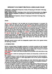
2.1. Divided Word Line Architecture Another solution to this problem is to split the WL into one global word line (GWL) and several local word lines (LWLs), as shown in Figure 1 [5]. The GWL connects to the LWLs through a local row decoder. A LWL covers only a part of the row in the memory array. The GWL is implemented in a higher metal layer than the LWLs, yielding a reduced capacitance. Also, since the GWL only connects to a row decoder instead of all cells on a row, the load capacitance of the GWL is reduced further. When using local row decoders, only one LWL is active in each memory access. This memory architecture is called the divided word line architecture.
2.2. Power Consumption in the Divided Word Line Memory Architecture The array current, shown in Equation 1, is the same for the divided word line architecture as for the simple array memory since the number of active and inactive cells are the same. The decoder current of the divided word line architecture becomes n I decoder = ------ ⋅ C GWL + n B ⋅ C LWL ⋅ V DD ⋅ f nB
where CGWL is the load capacitance of the global row decoder, CLWL is the load capacitance of the local row decoder, n is the number of words in the memory, and nB is the numbers of LWLs in the memory. CGWL can be kept small by selecting a suitable metal layer and wire width. Also, since only the local row decoders are connected to the GWL, this capacitance will be much smaller than CWL in the simple structure. The part of the current which is due to the local row decoders in Equation 3, nBCLWL, is valid if only the decoders on the active GWL consume current. Otherwise, it must be multiplied with n/nB.
2.3. Partitioned Memory Architecture Large memories can be divided into several, smaller memories, called partitions, using the partitioned memory architecture [7]. The small memories can, for example, be implemented as simple arrays, as shown in Figure 2. When a larger memory is required, the basic block is duplicated. The partitioned memory architecture yields smaller memory arrays, which reduces the complexity of the row decoders. However, block decoders must be added to select the correct partition.
PULLUP
ROW DEC
GWL
ARRAY
LWL SA WRITE
0
BLOCK DEC 0
GLOBAL ROW DEC
LOC ROW DEC
ARRAY nB -1
LOC ROW DEC
ARRAY 0
n/nB -1
Figure 1. Example of a divided word line architecture.
(3)
Figure 2. A basic block for the partitioned memory architecture.
2.4. Power Consumption in the Partitioned Memory Architecture As can be expected, the array current of the partitioned memory architecture is the same as for the simple array and the divided word line architecture since the number of active and inactive bits are the same. In this structure block and row decoders are used. These will affect the decoder current. The decoder current for the partitioned memory architecture, with simple arrays as partitions, is
P0
n P P-1 2
nP 2
Pn -1
P
P
n I decoder = ------ ⋅ C rowdec + n P ⋅ C blockdec ⋅ V DD ⋅ f (4) nP
MEM I/O
where n is the number of words in the memory and nP is the number of partitions. Cblockdec includes all capacitance a block decoder has to drive. The size of the memory arrays is traded for the complexity of the block decoder, i.e., the relative contribution from the two parts depends on the value of np.
2.5. Hierarchical Bank Structure The memory partitions can be connected through a so called hierarchical bank structure, as shown in Figure 3 [4]. This is a tree structure, for which each leaf is a number of memory banks. The banks are connected to decoders that only activates one bank in each cycle. Hence, only the block decoders of one partition will be activated in each cycle which reduces the decoder current. The result is that the decoder current will be of the same order as for one memory partition, shown in Equation 4. This structure also makes it possible to get a regular floorplan of the memory. This simplifies the implementation of the memory generator.
3. Implementation For the implemented memory generator the divided word line architecture, the partitioned memory architecture and the hierarchical bank structure has been combined. This combination was selected in order to obtain a low power consumption as well as a high design efficiency. For the smallest memories generated, up to 64 words, the simple array architecture is used. When the memory size increases, the divided word line architecture is used. Here such architecture is used for memory sizes between 64 and 128 words. The next step is to introduce the partitioned memory architecture, where one partition is composed by one divided word line structure. Hence, the partition size is 128 words. Two partitions are then combined into one memory bank to obtain larger memories, yielding a memory bank size of 256 words. Further increase of the memory size by factors of two is obtained by doubling the number of memory banks in each step.
Figure 3. Hierarchical bank structure. To determine the maximum size of the memory arrays, the number of LWLs in each array, and the size of the partitions, the circuits used in the memory has been evaluated. This has been done through simulations on the subcircuits in a environment that emulates the memory. The number of cells on a LWL is, for this implementation, equal to the number of bits per word, i.e., each LWL covers one word. The optimal number of LWLs on one GWL should yield acceptable speed and an aspect ratio of the block between 1 and 2. For the maximum data word lengths considered here, 48 bits, the optimal solution was found to be two LWLs, one on each side of a row decoder. In order to reduce the complexity of the generator design, this solution is used for all data wordlengths. This will, however, give an area overhead for memories with short data wordlengths. The generator is prepared for increasing the number of LWLs, if the area efficiency needs to be increased in the future. The maximum height of an array in the smallest building block is given by the pull-up circuit and the write circuit. An acceptable speed can be kept for blocks with up to 64 rows. For 128 rows, the speed degenerates. Also, it was shown that the row decoder, a clocked NOR decoder [3], can be implemented efficiently for up to 64 rows. This has been verified through simulations. Hence, a maximal array height of 64 is used. The aspect ratio of the memory was limited to be smaller than two, i. e., the height of the memory should never exceed two times the width of the memory. A reason for this is to obtain a memory with a regular structure, suitable for integration with as many digital designs as possible. This limits how many partitions that can be placed within each basic bank. The number of partitions will be doubled as
long as the total width is less then twice the height of the current memory. If the memory size has to be increased further, the new partitions are placed on a second row, below the current row. This block now becomes the basic bank. If the memory size is to be increased further, it is only possible by adding such a basic bank, yielding an increase of the memory size with a factor of two.
3.1. Implementation Example Figure 4 shows an example layout for a generated memory with a size of 4096 words and a wordlength of 36 bit. The height and the width of the example are 2.9 mm and 1.8 mm, respectively, and the area of the memory is 5.51 mm2. This gives a memory density of 28 kbit/mm2. This is due to the non-optimized memory cell used in the first version of the generator. In future versions of the generator, with optimized memory cells, a higher memory density can be expected. The example memory consists of 16 basic banks, i.e., 32 partitions. Figure 5 shows one memory bank with two partitions. From the figure the divided word line architecture of each partition, with one LWL on each side of the local row decoders, can be seen. The write time for this memory is estimated to 12 ns.
Figure 5. A memory bank composed of two partitions. generated memories can be up to 16kwords large with wordlengths between 8 and 48 bit. The main focus of the work has been to increase the design efficiency for design and implementation of RAMs. The power consumption has also been considered. A structure that combines the divided word line architecture, memory partitioning, and the hierarchical bank structure were found to be both design and power efficient.
5. References [1]
[2] [3]
[4] [5] [6]
[7]
Figure 4. Layout of a 4096 words SRAM with a wordlength of 36 bit.
4. Conclusions A layout generator for static memories has been developed. The generator is implemented in SKILL in order to be easily modified for more advanced processes. The current version use a standard, 0.18 µm, CMOS process. The
D. Capello, Design and Implementation of a Low-power Random Access Memory Generator, Master thesis, Linköpings universitet, LiTH-ISY-EX-3318, 2003. B. S. Amrutur., Design and Analysis of Fast Low Power SRAMs, dissertation, Stanford University, 1999. J. Caravella, “A Low Voltage SRAM For Embedded Applications”, IEEE Journal of Solid-State Circuits, vol. 32, pp. 428–432, March 1997. W. Ellis, Lecture notes in Semiconductor Memories, Linköpings universitet, 2003. B. Keeth and J. Baker, DRAM Circuit Design - A Tutorial, IEEE Press, New York, 2001. K. Itoh, K. Sasaki, and Y. Nakagome, “Trends in LowPower RAM Circuit Technologies”, Proceedings of the IEEE, vol. 83, pp. 524–543, April 1995. J. Rabaey, Digital Integrated Circuits - A Design Perspective, Prentice Hall, Upper Saddle River, New Jersey, 1996.