476
IEEE TRANSACTIONS ON RELIABILITY, VOL. 52, NO. 4, DECEMBER 2003
Design of a Fault Tolerant Solid State Mass Memory Gian Carlo Cardarilli, Member, IEEE, Alessandro Leandri, Panfilo Marinucci, Marco Ottavi, Salvatore Pontarelli, Marco Re, Member, IEEE, and Adelio Salsano, Member, IEEE
Abstract—This paper describes a novel architecture of fault tolerant Solid State Mass Memory (SSMM) for satellite applications. Mass memories with low-latency time, high throughput, and storage capabilities cannot be easily implemented using space qualified components, due to the inevitable technological delay of these kind of components. For this reason, the choice of Commercial Off The Shelf (COTS) components is mandatory for this application. Therefore, the design of an electronic system for space applications, based on commercial components, must match the reliability requirements using system level methodologies [1], [2]. In the proposed architecture error-correcting codes are used to strengthen the commercial Dynamic Random Access Memory (DRAM) chips, while the system controller is developed by applying fault tolerant design solutions. The main features of the SSMM are the dynamic reconfiguration capability, and the high performances which can be gracefully reduced in case of permanent faults, maintaining part of the system functionality. This paper shows the system design methodology, the architecture, and the simulation results of the SSMM. The properties of the building blocks are described in detail both in their functionality and fault tolerant capabilities. A detailed analysis of the system reliability and data integrity is reported. The graceful degradation capability of our system allows different levels of acceptable performances, in terms of active I/O link Interfaces and storage capability. The results also show that the overall reliability of the SSMM is almost the same using different RS coding schemes, allowing a dynamic reconfiguration of the coding to reduce the latency (shorter codewords), or to improve the data integrity (longer codewords). The use of a scrubbing technique can be useful if a high SEU rate is expected, or if the data must be stored for a long period in the SSMM. The reported simulations show the behavior of the SSMM in presence of permanent and transient faults. In fact, we show that the SCU is able to recover from transient faults. On the other hand, using a spare microcontroller also hard faults can be tolerated. The distributed file system confines the unrecoverable fault effects only in a single I/O Interface. In this way, the SSMM maintains its capability to store and read data. The proposed system allows obtaining SSMM characterized by high reliability and high speed due the intrinsic parallelism of the switching matrix. Index Terms—Codes, memory architecture, redundancy, self checking, solid state mass memory, SSMM.
ACRONYMS1 EDAC IMAM MCM
Error Detection And Correction Independent Memory Array Module Multi Chip Module
Manuscript received January 1, 2002; revised March 1, 2003. G. C. Cardarilli, A. Leandri, M. Ottavi, S. Pontarelli, M. Re, and A. Salsano are with the Department of Electronic Engineering University of Rome “Tor Vergata”, Italy (e-mail:
[email protected],
[email protected],
[email protected],
[email protected],
[email protected]). P. Marinucci is with Consorzio Ulisse (e-mail:
[email protected]). Digital Object Identifier 10.1109/TR.2003.821938 1The
singular and plural of an acronym are always spelled the same.
MKU SCU SSMM
Memory Kernel Unit System Control Unit Solid State Mass Memory NOMENCLATURE
BER LT MTTF MTTR R(t) SER
Bit Error Rate Latency Time Mean Time To Failure Mean Time To Repair Reliability function Symbol Error Rate I. INTRODUCTION
T
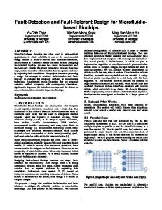
HE DESIGN of electronic systems for space applications must consider several problems related to the harsh environment in which they operate. In fact, in the space environment the electronic components are stressed by a large number of physical phenomena, like mechanical stresses, ionizing radiations and critical thermal conditions. To face these specific application constraints, the typical approach has been the development of space qualified electronic devices based on special and expensive technology processes. The use of such components implies some important drawbacks such as the high cost and the low performance available compared to the Commercial Off The Shelf (COTS) components [3]. Therefore, the design of an electronic system for space applications using commercial components must fulfill the reliability requirements following suitable system level methodologies. A typical application, where this approach is exploited, is the design of space-borne mass memories. In fact, the rapid growth in capacity of semiconductor memory devices permits the development of solid-state mass memories, which are competitive with respect to tape recorders due to higher reliability, comparable density and better performances. Solid-state mass memories have no moving parts and their operational flexibility has made them suitable for many applications. Moreover, the requirements of low latency time, high throughput, and storage capabilities, cannot be satisfied by space qualified components and the choice of COTS is mandatory. The SSMM presented in this paper is based on COTS components. In the proposed architecture a number of SpaceWire data links [4] access the memory banks through a cross-point switch matrix [5]. This solution is convenient with respect to a bus based architecture in terms of bandwidth, latency and reconfiguration capability. In fact, the failure of a connection does not compromise the entire connection of the network but only the access to a specific node. Moreover, to improve both the fault tolerance and the memory usage, we implemented a distributed file system on the SSMM. Most of the functions performed by the file system are hardware based and handled locally on each
0018-9529/03$17.00 © 2003 IEEE
Authorized licensed use limited to: UNIVERSITA DEGLI STUDI DI ROMA. Downloaded on May 13,2010 at 15:17:06 UTC from IEEE Xplore. Restrictions apply.
CARDARILLI et al.: DESIGN OF A FAULT TOLERANT SSMM
477
memory module. This paper is organized as follows: Section II illustrates the used design methodology. Section III describes in details the SSMM architecture, while reliability evaluation and the results of system simulation are given, respectively, in Section IV and Section V. II. DESIGN METHODOLOGY OF FAULT TOLERANT SYSTEMS This section describes the design methodology followed for the implementation of the fault-tolerant SSMM. We focus our attention on the typical fault set defined for the space environthe Single Event Upset (SEU) faults, caused by ionment izing particles, and stuck-at faults, related to the Total Ionizing Dose (TID) [6], [7]. The design of fault tolerant systems can be made in different ways, depending on the number of constraints which the implementation must fulfill. The design is basically composed of two main tasks which must be interdependent: • matching of the specs in terms of performance and functionality, and • application of the suitable design strategies for obtaining the requested reliability. The fault tolerance design methodologies applied, when COTS are used, are basically two: fault masking, e.g., Triple Modular Redundancy (TMR) [8] or, when the application needs low hardware overhead, fault detection and dynamic system recovery techniques. The latter method satisfies the requirement of a lower hardware redundancy and lower power consumption, with respect to TMR technique, but, on the other hand, needs reconfiguration algorithms (software redundancy) and, when a fault occurs, implies an out-of-order time interval related to the Mean Time to Repair (MTTR). Moreover, the use of dynamic reconfiguration algorithms allows a graceful degradation of the system. In fact, after the detection of an unrecoverable fault, the system can be modified to keep it working, even if its performance or functionalities are generally reduced. This methodology can be easily applied for the realization of SSMM for space applications, where the constraints on power and weight are quite relevant and the system can tolerate the presence of an out-of-order time when time-critical operations are not performed. A hierarchical fault tolerant design methodology has been used achieving dynamic reconfiguration and graceful degradation of the system. In fact, at each level of the hierarchy, a module controller can be instantiated to check the local functionality. The module controllers must be designed by using high reliability techniques, avoiding single points of failure because the reliability of the whole system could be compromised in case of faults. The implementation of subsystems with adequate levels of reliability can be made on reprogrammable devices, like Field Programmable Gate Array (FPGA) or System on Chip (SoC), which allow flexible reconfiguration methodologies [9], [10]. Moreover, reprogrammable devices allow the fast prototyping of the system reducing the nonrecurrent costs with respect to an ASIC implementation. System decomposition into self-checking functional blocks allows a fine-grained fault localization and isolation with system level procedures. This fine-grained fault localization allows us to reduce the MTTR in case of recoverable faults, and to improve the graceful degradation of the system in case
Fig. 1. External SSMM connections.
of unrecoverable faults. In fact, increasing the granularity of fault detection, only a few logic resources or functional blocks can be put off-line. III. ARCHITECTURE DESCRIPTION In this section, a detailed description of the SSMM architecture is presented. This architecture has been designed following the approach described in Section II. At the top level, the SSMM can be viewed as a black box connected to different satellite apparatuses (Fig. 1). A number of bi-directional serial links are used for high-speed data exchange. For these links the Spacewire (IEEE 1355 DS-DE) protocol [11] has been chosen. In fact, Spacewire is planned to become a European Space Agency (ESA) standard for on-board data-handling in the near future and is expected to be widely used in future European missions [4], [12]. Each Spacewire link carries information (data or commands) at about 100 Mbit/sec over distances of up to 10m. Moreover, the SSMM is connected with a MIL 1553 bus, which is widely used in satellite platforms due to its physical redundancy (dual twisted pair bus structure) [13]. Two main units compose the SSMM architecture (Fig. 2): 1) The Memory Kernel Unit (MKU) manages the bi-directional data flow between users, & memory chips. 2) The System Control Unit (SCU) manages the memory resources, and provides system level reconfiguration. The required reliability of the SSMM system is achieved both by means of architectural redundancies, and by introducing Error Detection And Correction Codes (EDAC), granting the data integrity. In (Fig. 3), for each unit are indicated the composing subunits and in the bottom row, the adopted fault tolerant technique. In the following pages each block of the architecture will be described. A. Memory Kernel Unit: General Description As shown in Fig. 2 the Memory Kernel Unit is composed of four functional modules: 1) Independent Memory Array Modules (IMAM) (see Section III-A-I), 2) Routing Module (see Section III-A-II),
Authorized licensed use limited to: UNIVERSITA DEGLI STUDI DI ROMA. Downloaded on May 13,2010 at 15:17:06 UTC from IEEE Xplore. Restrictions apply.
478
IEEE TRANSACTIONS ON RELIABILITY, VOL. 52, NO. 4, DECEMBER 2003
Fig. 2. SSMM architecture.
Fig. 3.
Fault tolerance techniques.
3) I/O Link Interfaces (see Section III-A-III), and 4) I/O Memory Interfaces (see Section III-A-IV). The memory kernel unit under the SCU control provides all the resources for the implementation of a file system on the set of SDRAM modules. The I/O Interfaces are divided into two groups: I/O Link Interfaces and I/O Memory Interfaces. The I/O Memory Interfaces handle the IMAM file system, allowing basic operations like file read/write, delete, format etc. The I/O Link Interfaces are the front end of the system, providing a bi-directional transport of data and messages. The packet routing control and the dynamic reconfiguration of the
system in case of faults are handled by exploiting the HW/SW interaction between these interfaces and the SCU. Once a connection between two interfaces is established, the data flow control is achieved through full handshake. The Routing Module is the central switch which interconnects the users (I/O Link Interface) with the memory modules. All I/O Link Interface and Memory Interface modules are connected to the SCU through a message bus (MsgBus) which allows communication of either the detection of a fault, or the necessary messages to operate the packet routing control (Fig. 2). Each module has been developed using different fault tolerant methodolo-
Authorized licensed use limited to: UNIVERSITA DEGLI STUDI DI ROMA. Downloaded on May 13,2010 at 15:17:06 UTC from IEEE Xplore. Restrictions apply.
CARDARILLI et al.: DESIGN OF A FAULT TOLERANT SSMM
Fig. 4.
479
Memory array architecture.
gies, depending on the final reliability requirements and the functionalities performed. These choices will be described in Sections III-A-I–IV together with a detailed description of the modules. 1) Independent Memory Array Module (IMAM): The design of the memory array with COTS RAM chips (DRAM) requires an accurate characterization of the used components in the environment in which they will operate. The effects of ionizing radiations on DRAM memory chips can be widely found in literature [3], [15], [16]. As we will show in Section IV, the application of error correcting codes strengthen the IMAM both in terms of reliability and data integrity. Each IMAM module is composed of • a Dynamic Random Access Memory (SDRAM) bank (composed of several COTS chips or MCMs), • a Control circuitry that interfaces the memory bank to the other components of the IMAM module, and • a Reed-Solomon (RS) coder-decoder which adds redundancy to the data stored into the SDRAM. The IMAM architecture is shown in Fig. 4. The SDRAM packages are arranged on 4 rows per board side and each row is composed of 18 packages. Each package implements an 8 bit symbol. Using both the sides of the board, we
are able to implement either a Reed Solomon (RS) code with a maximum codeword length of 144 symbols (2 sides 4 row 18 column 144 SDRAM packages) or a code with a minimum codeword length of 18 symbols. The data word length depends on the reliability and data integrity constraints. The IMAM is able to support either variable dataword and/or codeword length. The RS encoder is based on the work presented in [17]. The encoder architecture is shown in Fig. 5 where the number of the registers used depends on the code length. The decoder block is realized by a four stage pipeline as shown in Fig. 6. The most important codec features are • the small area occupancy due to the methodology proposed in [18] and “time-sharing” techniques that have been successfully applied to finite response filter applications [19], • the optimization of the decode latency as illustrated in [20], and • a low cost reconfiguration: the codec can be reconfigwith (36,32) (72,64) ured as RS (144 128). , for all the used codes, is 0.89 i.e., the check The ratio byte overhead is constant with respect to the selected code.
Authorized licensed use limited to: UNIVERSITA DEGLI STUDI DI ROMA. Downloaded on May 13,2010 at 15:17:06 UTC from IEEE Xplore. Restrictions apply.
480
IEEE TRANSACTIONS ON RELIABILITY, VOL. 52, NO. 4, DECEMBER 2003
Fig. 5. Encoder architecture (conventional).
Fig. 6. Decoder block diagram (4-stages pipeline).
Suppose we have random errors and that erasures occur. The following equation indicated by maximum correction capaRS codes [20]: bility should be satisfied in
RS code reconfiguration is used when a permanent failure occurs in a memory package. For example, if the SSMM is initially configured with an RS (18,16) code and a permanent failure occurs in a memory package, the code can’t correct any random
error. Therefore we need to reconfigure the memory module with a new RS code. For example a RS (144 128) code is able to correct the 8 erased symbols and is also able to correct upon 4 random symbol errors. Otherwise, if a fixed RS code is used, the module memory shall be in permanent fault and the only possible strategy is its substitution with a spare module. Permanent package failures can be easily detected by applying a reading and decoding procedure. The decoded (and corrected) data will be coded again with a RS code with higher correction capabilities. To perform this operation, a suitable buffer temporarily stores the codewords that will be grouped to form the larger one. Obviously, the use of a higher RS code involves the use of a higher number of symbols. On the other hand, the fixed ratio allows the use of higher RS code without adding symbols overhead. As an example we show the reconfiguration from the RS (36,32) to the RS (144 128). Starting from a RS (36,32) coding scheme, after a certain period of time, the check procedure detects three permanent package failures (three erasures). All the data stored in the memory module are converted from RS (36,32) to RS (144 128): for example, four 36 byte codewords are read & decoded and the 128 data bytes are coded into a codeword of 144 bytes. This procedure allows preserving the data stored in the memory. However, if the number of erasures is greater than the error correction capability of the active code, (for example, 5 erasures for the RS (36,32) code), the data stored in the codeword are unrecoverable; but the functionality of the memory element can be restored using a code with greater error correction capability. The use of longer codewords improves the integrity of the stored data degrading the performance of the IMAM in terms of latency. In fact, the decode latency depends on the codeword length. 2) Routing Module: The routing system connects the I/O Memory Interfaces with the I/O Link Interfaces through a crossbar switch matrix. The interconnection is performed in nonblocking mode. An arbiter provides the acknowledge signals to the I/O interfaces that send data through the crossbar. The main blocks composing the routing module are: • a crossbar switching matrix, and • an access arbiter.
Authorized licensed use limited to: UNIVERSITA DEGLI STUDI DI ROMA. Downloaded on May 13,2010 at 15:17:06 UTC from IEEE Xplore. Restrictions apply.
CARDARILLI et al.: DESIGN OF A FAULT TOLERANT SSMM
481
Fig. 7. Distributed arbiter.
With this interconnection method multiple parallel connections between users and resources can be established, increasing the overall throughput. Latencies can be reduced choosing appropriate arbitrating policies. Moreover, the intrinsic redundancy of such architecture increases the reliability of the system. The failure of a connection, due to a fault in an I/O interface or in a switch, implies only a partial loss of the system functionality. a) Crossbar Switch Matrix: This component allows the physical interconnection among I/O Link Interfaces and I/O Memory Interfaces (see Fig. 2 ). The number of the possible connections, and thus the number of switches and wires necessary in a crossbar switch matrix can be defined by introinterconnection matrix where . In ducing a element is equal to 1 if there is a connection this matrix the between the input and the output and 0 if the connection is not present. In particular, for this matrix we can distinguish three typical cases and evaluate the number of switches and wires of crossbar matrix implementing the connection. 1) Complete connection: every input is connected with every output:
requires switches and wires. 2) Without loopback: no connection between and if
requires switches and wires. 3) With I/O subsets: In this case we consider two subsets of the set of I/O interfaces: and of and elements and respectively, being . Connections are only present between elements belonging to different subsets. This case requires switches and wires. The Solid State Mass Memory routing system doesn’t need a full connection between all users, thus a connection of type 3) could been used. However, the choice of the switching matrix can be seen like a trade-off between area overhead and performance/reliability. In fact, the use of a topology like that
of 3) reduces the area overhead of the matrix but implies that, if a connection fails, the bi-directional communication between two interfaces is no longer possible. Therefore, because the implementation of the general-purpose switch connection 1) doesn’t introduce high overhead with respect to the topology of 3), while granting more flexibility in the connections available, the switching matrix is implemented with this topology. Moreover, the loopback connections can be exploited to evaluate the correct operations of the single interfaces in test mode. b) Arbiter: The arbiters handle the interconnections between I/O interfaces. The use of a single arbiter to manage all the interconnections represents a single point of failure. Therefore we implemented an arbiter for each shared output. This method implies another advantage respect to a centralized arbiter; in fact it is easier to set different arbitrating policies for each output. In Fig. 7 we show the scheme of the switch matrix with the embedded arbiters for each output. The figure represents only the connections from I/O Link Interfaces to I/O Memory modules for sake of simplicity Each I/O interface handshakes the request of an output with the arbiter. The signals involved are a request (REQ) emitted by the interface and an acknowledge (ACK) generated by the arbiter. The possible arbitrating policies are priority-based or time-sharing. In the first case, only some I/O Interfaces have more bandwidth available (e.g., During the window of visibility of a Low Earth Orbit (LEO) satellite the I/O Memory Interfaces that are downloading the data to the earth station must have more bandwidth assigned). In the other case the bandwidth is almost equally shared between the interfaces. 3) I/O Link Interfaces: As stated above, the I/O Link Interfaces provide the transport of data and messages between users (i.e., the data collecting instruments, the remote control circuitry) and the memory modules. The structure of the packets exchanged with the spacewire interface is composed of three parts: header, payload, End Of Packet (EOP). The header is one byte long, and indicates the ID of the packet while the payload is composed of a variable number of bytes terminated by the End Of Packet (EOP) marker. We assume that header values in the range of 1 to 255 indicate that the packet is part of a file whose ID number is the header value. The header value 0 indicates a
Authorized licensed use limited to: UNIVERSITA DEGLI STUDI DI ROMA. Downloaded on May 13,2010 at 15:17:06 UTC from IEEE Xplore. Restrictions apply.
482
IEEE TRANSACTIONS ON RELIABILITY, VOL. 52, NO. 4, DECEMBER 2003
Fig. 8.
I/O link interface. Fig. 9.
special packet containing commands or diagnostic communications sent or received from the memory. Thus the file system can handle 255 files and the memory can be controlled and monitored using the same links carrying the data. Most of the I/O Link Interfaces are unidirectional. These interfaces correspond to the links carrying the measurement information. A small number of interfaces requires reading and writing of the memories. One of the most important interfaces connects the memories to the telemetry circuitry. This circuit transmits collected information from the satellite to the earth station. All the interfaces access the switch matrix in full-duplex mode, and request arbitration through dedicated links. An internal shared bus interconnects all the I/O interfaces and the microcontroller to provide file system management and error detection. A generic I/O link interface is composed of two main functional blocks (Fig. 8): the “Data Routing Block”, that handles the data flow, and the “Interface Controller” block, that connects the interface with the System Control Unit and provides also local error handling with the “Error Handler” function. The main functions of the “Data Routing Block” are the following: • LVDS I/F. This block implements the electric interfacing between the differential signals LVDS (Low Voltage Differential Signaling) and Data and Strobe single ended signals. • SpaceWire (1355 DS-DE) I/F. This interface interprets the serial signal, implements the flow and the parity control following the procedures of the SpaceWire protocol, extracts the clock signal and pushes the extracted data into the FIFO in parallel mode. The parallelism of the data is 8 bit + 1 flag bit to separate a data/header token from an EOP marker. • FIFO. The FIFO depth must be chosen to avoid data loss due to the latency of the successive subsystems. Because serial link can reach 100 Mbps, the FIFO speed is up to 10 Mtps (Mega tokens per second, with 10 bits per token). • LINK I/F. This block represents the core of I/O Link interfaces. It is composed of master and slave. The master
I/O memory interface.
block manages a local table of 255 elements containing the dynamically reconfigurable output association for each file. The entries of the table are written by the SCU through the “Message Handler” block. Once the output association is set the master negotiates the output connection with the arbiter. 4) I/O Memory Interfaces: These interfaces handle the file system. Each I/O Memory Interface has a local File Allocation Table (FAT) stored in the controlled memory module. The partition of the file system in every module reduces the amount of data which can be lost in case of an unrecoverable failure in the FAT. In fact, in case of failure we will only lose locally stored information. This macro-block is composed of a number of components as shown in Fig. 9. To handle the file system the memory interface implements the following functions: • Delete function: used to delete a file from the FAT • Fragment function: used to add to the FAT the occurrence of more fragments of the same file • Read function: used to read a file from the memory • Write function: used to write a file to the memory • Format function: used to set-up the FAT in the initialization phase Each function is implemented with a separate block and the “Operation Handler” inside the Interface Controller performs the activation of each function. Moreover, each functional block is self-checking and a spare block is used to obtain fault tolerance. In fact, because the occurrence of a failure on a single block can be detected, the “Error Handler” inside the Interface Controller can activate the spare module with a low time overhead. Both the “Operation Handler” and the “Error Handler” communicate with the rest of the SSMM through the message handler that is the third block composing the Interface Controller. Therefore, through the message bus, the SCU can control the status of each I/O Memory Interface both in the case of normal function and in the case of fault occurrence. To obtain single point of failure avoidance, the Interface controller has been implemented with TMR technique.
Authorized licensed use limited to: UNIVERSITA DEGLI STUDI DI ROMA. Downloaded on May 13,2010 at 15:17:06 UTC from IEEE Xplore. Restrictions apply.
CARDARILLI et al.: DESIGN OF A FAULT TOLERANT SSMM
483
Fig. 10. System control unit.
B. System Control Unit The System Control Unit (Fig. 10), manages the access of the users and the resources of memory. This module is connected with the rest of the SSMM system through the internal communication Bus MsgBus, used for the communications service, and through the selection signal Sel that regulates the modality of access to the MsgBus. The Bus_IF interface handles the exchange of messages between the controller and the rest of the SSMM system through the MsgBus. The system uses two Intel 8051 microcontrollers which can be connected or isolated from the system through the block Bypass. Normally only a single processor is active and connected to the system, while the other one is in stand-by and electrically isolated. The active microcontroller accesses a 2k ROM memory, which contains the executable program, and to a 1K RAM memory that is used for the data storage and management. The Mem_IF block supplies the coding of the data the microcontroller writes in the RAM. The data read from the memory is decoded from the same block. The operation performed by the Mem_IF is transparent to the microcontroller. The “Address handler” block handles the connection between the microcontroller and the Mem_IF and Bus_IF creating the suitable switches, transparently to the microcontroller, to achieve the required connections. The “Signature calculation” block controls the correctness of the operations performed by the microcontroller. This block reads the sequence of the addresses output by the microcontroller and verifies they are following a correct sequence. The evaluation of the correct execution is performed with a specific application of a well-know fault detection technique called signature analysis [21], [22].
The “Operations handler” block manages the phases of the elaboration of a message. If some phases are not executed correctly, this system supplies the relative error signaling. The “Error handler” block receives error signals from all the blocks of the system and handles the error exceptions. It operates in a transparent way, and assumes the control of the system only if an error is found. The error management is aimed to mask the system faults. If the error persists, the manager can substitute the active microcontroller with the spare one. IV. RELIABILITY AND DATA INTEGRITY EVALUATIONS In this section some evaluations of reliability and data integrity of the SSMM are shown. The IMAM dominates the complexity of the system. In fact, to obtain a storage capacity of several Gigabytes, a high number of SDRAM chips must be used. Therefore, the reliability of this subsystem must be accurately studied. Moreover, the use of RS codes to grant a high level of data integrity allows an increase in the reliability of the IMAM. In fact, the erroneous data of a failed SDRAM chip can be viewed as particular data errors, called erasure, and corrected by the RS codec. This improvement of the reliability depends on the codeword length and on the memory scrubbing frequency. A. Solid State Mass Memory Reliability Evaluation The allocation of reliability to a system involves solving the basic inequality:
where is the allocation reliability parameter for the -th subis the system reliability requirement parameter and system, is the functional relationship between subsystem and system reliability.
Authorized licensed use limited to: UNIVERSITA DEGLI STUDI DI ROMA. Downloaded on May 13,2010 at 15:17:06 UTC from IEEE Xplore. Restrictions apply.
484
IEEE TRANSACTIONS ON RELIABILITY, VOL. 52, NO. 4, DECEMBER 2003
Fig. 11.
Reliability model of the solid state mass memory.
Fig. 12.
Reliability model of the IMAM configured with RS (36,32).
For a simple series of systems, in which the ’s represent the probability of survival at End Of Life (EOL), we get
The above equation has an infinite number of solutions and a procedure that yields a unique or limited number of solutions must be used. For this purpose we use a proprietary optimization tool [23] based on the minimization of an Effort Function, as described in [24]. For the reliability evaluation of the SSMM the reliability model shown in Fig. 11 is used. Each block represents a subsystem where the numeration corresponds to: • 1—SCU; • 2—Routing Module; -th IMAM; • MM -th Spare IMAM; • MMS The Error handler and the bypass blocks of the SCU allow switching to the cold spare microcontroller when a permanent fault is detected. Thus, the SCU subsystem can be seen, in a coarse estimation, as the parallel of two blocks, if we assume the switch and the checker as ideal. An estimation of the reliability of the routing module should consider the graceful degradation capability of the module. An example of such approach can be found in the literature [29], [30]. In this section, we evaluate the lower bound of the routing module reliability approaching it in the same way of the SCU module. This approach means that the reliability evaluation of the SSMM is referred to the system without performance degradation.
To evaluate the reliability of the IMAM we must decompose the subsystem depending from the choice of the used RS code. Figs. 12 and 13 describe the reliability model for the configurations RS (36,32) and RS (72,64), showing the series and parallel connections needed to provide the reliability expression for the IMAM. Each block represents a subsystem where the numeration corresponds to: 3—Partition driver. 4—Mem. Module Front End Electrics; 5—Mem. package hardware (Buffer, LCL,…); 6—SDRAM stack; 7—EDAC; 8—Memory module controller; Now we can define the component reliability function as: (1) where is the mission time and is the component failure rate . (in failure/ The Component failure rate can be estimated using the models reported in Table I. The factors present in the models are the stress parameters and base part failure rate values. The factors for failure rate calculation are reported in Table II. To calculate the reliability of the IMAM we apply the following equations: Hot redundancy ( -out-of- structure) (2)
Authorized licensed use limited to: UNIVERSITA DEGLI STUDI DI ROMA. Downloaded on May 13,2010 at 15:17:06 UTC from IEEE Xplore. Restrictions apply.
CARDARILLI et al.: DESIGN OF A FAULT TOLERANT SSMM
485
Fig. 13. Reliability model of the IMAM configured with RS (72,64). TABLE I FORMULAS FOR MICROCIRCUIT RELIABILITY
TABLE III SUBSYSTEMS FAILURE RATES
TABLE II FACTORS FOR FAILURE RATE CALCULATION TABLE IV RELIABILITY EVALUATION OF THE SSMM
where is the number of units and is the number of units needed for the correct functionality. Cold redundancy (ideal switching module): (3) where is the failure rate of the active components, is the failure rate of the components in standby (by assumption), is number of units, is the number of units needed for the . correct functionality and Cold redundancy out of nonideal switching module
(4) are the failure rates of the active components and where is the failure rate of the components in standby. Notice that, in the reliability estimation, we include the failure rate of the components in standby. This approach gives a more realistic system modeling, because the various parts of the system are active only for a fraction of the system life. As an example, we consider the following configuration of the SSMM:
• Five active memory modules, each module having 576 MBytes including the code symbols, and a cold spare one; • MCM-V memory packages with two layers; • 144 MCM-V on every PCB; and • EDAC with the code RS (36,32) and RS (72,64). We want to obtain the reliability after 2 years for two different configurations of the RS codec i.e., RS (72,64) and RS (36,32). We use the subsystems’ failure rates reported in Table III, where for the components 1 and 2 we apply the formulas given in Table I. In Table IV, we report the results of the reliability after 2 years obtained for the two code configurations applying the above formulas. The above results show that the architecture has a reliability level matching the requirements of a two-year long satellite mission. Notice that the overall results are related to the hypothesis of full functionality of the SSMM after 2 years. However, the graceful degradation capability of our system allows different levels of acceptable performance; for example, the SSMM can
Authorized licensed use limited to: UNIVERSITA DEGLI STUDI DI ROMA. Downloaded on May 13,2010 at 15:17:06 UTC from IEEE Xplore. Restrictions apply.
486
IEEE TRANSACTIONS ON RELIABILITY, VOL. 52, NO. 4, DECEMBER 2003
proximation derived in [25] to calculate the BER after the correction operations:
TABLE V NOTATION
(6) For messages with bit symbols and for perfect error correction codes we can extend the approximation derived in [25] to calculate the Symbol Error Rate (SER) after the correction operations: be reconfigured to work also with less I/O link Interfaces and/or memory modules. Therefore the above evaluations can be considered as a worst case analysis of the system, while the probability that the SSMM keeps working at the end of mission with reduced performance is quite higher as explained in [32]. Analyzing the results in detail, we can notice that the reliability of the memory control for the RS (36,32) configuration is better than RS (72,64); however the latter can tolerate a larger number of memory package failures. Therefore, the overall reliability of the RS (72,64) configuration is almost the same as the other case. The modification of the RS coding scheme improves the data integrity as we will show in Section VI-B. B. Data Integrity Evaluation To evaluate the data integrity of the system we use the notation adopted in [14], [25] and reported in Table V. we assume the following: 1) Transient faults occur with a Poisson distribution. 2) Bit failures are statistically independent and thus linearly uncorrelated. 3) The control, correction, and interface circuitry in the memory system are fault-tolerant. 4) There is a dominant memory bit cell failure mode. This assumption, with assumption 3, provides an upper bound on system reliability. A theoretical model of the mass memory can be applied to evaluate the data integrity. The memory is modeled as a transmission channel [14], [25]. During the latency period the noise corrupts the integrity of data. If the noise is generated by SEU, of data and it is given the BER depends on the latency time by (5) where is the rate of occurrence of SEU and depends on radiation environment and device technologies [29].
(5) The correction device performs the error correction function as the inverse operation of noise source. It uses the correction data (output of the virtual observer) and the channel output to restore data integrity. For messages with one bit symbol, and considering perfect error correction codes, we can use the ap-
(7) if where If the BER after a single memory correction (i.e., memory scrubbing) is given by (8) Derivation of BER approximation for memory subsystem with scrubbing: perfect code (as This memory subsystem uses a random errors) Reed Solomon code, able to correct and scrubbing procedure. Periodically the whole memory is acerrors are cessed and it is checked for correctness. If detected the word is corrected and rewritten in its original location. An uncorrectable word error occurs and memory subsystem fails, if the errors accumulated in one word exceed the ). If we assume that correction capability of EDAC (i.e., if the errors are distributed randomly over the address space, the number of erroneous bits at j-th scrubbing is given by
(9) where: represents the scrubbing cycle, • • represents the number of intervals of deterministic scrub, bing represents the corrupted bit after at start of • -th scrubbing, and represents the number of errorless • -th scrubbing. bits after In (9) we included the corrupted bits flipped to correct value. A SEU causes the switching of the state of a memory cell. If a cell has a corrupted value then the occurrence of a SEU causes the transition to its original value. Equation (9) provides the number of corrupted bits after j-th scrubbing as the sum of:
Authorized licensed use limited to: UNIVERSITA DEGLI STUDI DI ROMA. Downloaded on May 13,2010 at 15:17:06 UTC from IEEE Xplore. Restrictions apply.
CARDARILLI et al.: DESIGN OF A FAULT TOLERANT SSMM
TABLE VI BER @ STORAGE PERIOD OF 48 HOURS AND T
T
@
T
TABLE VII
= 2
DAY AND
BER
487
= 1000 Sec
T
@
T
TABLE VIII
= 2
DAY AND
BER
= 10
(2 MEM. PACKAGE FAILURE)
= 10
(0 MEM. PACKAGE FAILURE)
• corrupted bits ) that are not flipped to the -th and correct value by a SEU occurred between -th scrubbing, and -th and -th scrub• corrupted bits occurred between bing that are uncorrectable by EDAC. Therefore, the obtained BER at the end of -th scrubbing is given by
(10)
Fig. 14.
(11) If
we can simplify the (11)
(12) – erIn interplanetary space a background rate of rors/bit/day can be assumed, which occasionally increases up to – errors/bit/day during solar flares. The following tables summarize the data integrity evaluation in terms of BER from the minimum SEU rate to the maximum SEU rate, even if some package failures occur. In Table VIII the equations used for the BER calculation were: • for RS (36,32) , • for RS (72,64) . The above reported results show that the SSMM is able to tolerate a high number of permanent and transient faults occurring in the IMAM exploiting the RS coding reconfiguration. The reconfigurability of the RS code allows, given an expected SEU rate and a BER requirement, to operate both on
SSMM Design Flow.
the codeword length and/or the scrubbing period to obtain the requested memory performances. The choice of the codeword length and of the scrubbing period is the result of a trade-off. In fact the use of long codewords increases the time for decoding the data-word, while the use of short scrubbing periods increases the time in which the memory can’t be accessed by the user. Finally, we can notice that, as shown in Table VIII, with some combinations of SEU rate package failures and coding scheme, the scrubbing techniques are not necessary if we suppose that the memory contents are downloaded to an earth station every two days. V. SIMULATION RESULTS The simulation of the system was performed to test any single component composing the SSMM with suitable test benches for determining both its performances and its fault tolerant capabilities. The simulations have been performed in the design phase using VHDL language. To have a closer emulation of real physical faults, we injected faults in post-synthesis structural VHDL [26], [27]. The results obtained by behavioral and post-synthesis with fault injection simulations of the system gave us feedbacks in the design flow (Fig. 14). The simulation results reported here show the capability of the system to have a graceful degradation of its performances
Authorized licensed use limited to: UNIVERSITA DEGLI STUDI DI ROMA. Downloaded on May 13,2010 at 15:17:06 UTC from IEEE Xplore. Restrictions apply.
488
IEEE TRANSACTIONS ON RELIABILITY, VOL. 52, NO. 4, DECEMBER 2003
Fig. 15.
SCU without fault injection.
in case of faults. This is a further feature of the system that exploits the concurrent error detection capability of the architecture to improve its performability [32], [33] for a given level of reliability. In Section V-A we will show the behavior of the MKU and of the SCU units when they recover from fault occurrence. We will compare the normal behavior and the recovered one after detection. A. SCU Simulation The system control unit test has been made with a suitable online injection fault method based on a VHDL model of the SCU. During the normal operation of the SCU system, we injected a single error in order to simulate the random Single Event Upset (SEU) due to radiation that may occur in a space environment. The targets of this error injection were all the internal microcontroller special function registers and RAM locations. The injected errors were generated with uniform distribution in both logical addresses and time locations into a predetermined range. The normal SCU operation is composed of two operations: during the first operation, the SCU receives a write file request; in the second operation the SCU system receives a report that a block of pages has been allocated. The injection of a single SEU happens randomly during one of these operations. Fig. 15 shows the normal execution of both operations described above. The signals Mop and Nop represent that a new operation must be performed by the microcontroller. When both the signals become low, the microcontroller starts a new operation. The ERF signal represents the occurrence of a signature error, while port 3 represents the microcontroller port used to handle the interrupts and the control signals. finally, RAMI and BI are signals used to inject errors in VHDL. The simulation can be described as follows: first the SCU system reads the request message from the MsgBus (1); second the request message is handled and the SCU stores local data in the external RAM memory (2), while,
during the last step (3), the answer message is generated. The write file request operation is closed when both Mop and Nop signals come back high. The second test operation starts when both signals Mop and Nop become again low and is composed of three steps like the first operation. The block allocation operation starts with message request reading (4); this step is identical for both first and second test’s operations. The computing of received request continues though elaboration process (5) and terminates with the emission of end signal (6). This signal is used to communicate to all state machine of SCU system the end of a message processing that normally doesn’t need the generation of an answer message. The end of test occurs when both Mop and Nop signals become again high. Fig. 16 shows how the SCU system handles the error recovery. As shown in the last two lines of the waveforms of Fig. 16, the injection of a SEU is performed during the third step of first phase of the test. In this case, the injected fault affects the Stack Pointer register of the microcontroller thus the error is revealed by “error handler” that generates the signal ERF signaling that a wrong signature has been generated by the sequence of operations performed. The “error handler” starts the recovery algorithm forcing the repetition of all the steps of the phase affected by the error. The detection forces MOP low, requesting the repetition of the last operation. In fact, in Step (4) the packet is reloaded by the microcontroller; in step 5 the elaboration of the request is performed again; and, finally, in step 6 the phase is terminated correctly and the signals MOP and NOP go high. The test ends correctly performing the second phase that is not affected by the error injection. B. MKU Simulation The validation of the Memory Kernel unit has been done simulating the occurrence of unrecoverable failure in a memory module or in an I/O Memory Interface. In both cases the MKU must switch the data path from the out of order memory module
Authorized licensed use limited to: UNIVERSITA DEGLI STUDI DI ROMA. Downloaded on May 13,2010 at 15:17:06 UTC from IEEE Xplore. Restrictions apply.
CARDARILLI et al.: DESIGN OF A FAULT TOLERANT SSMM
Fig. 16.
SCU fault injection test.
Fig. 17.
Fault detection and re-routing.
to another one preventing the loss of data. Due to the system symmetry, the same reconfiguration can be done also if a failure occurs on an I/O Link Interface. This last feature exploits the capability of the system to read the data stored in the memories from any I/O Link Interface. The steps that compose the failure recovery routine are the following: 1) The failure is detected by the module due to its selfchecking capability, 2) The SCU receives the error signal, chooses another target memory module for the data and signals the new output for the I/O Link Interfaces connected to the out of order module. 3) The Routing Module switches the data path accomplishing the requests of the I/O Link Interfaces. In Fig. 17 are shown the waveforms corresponding to a data transfer from two link interfaces to two memory modules. In particular, file one coming from link one is routed to module one while file two, coming from link two is routed to module two. At a time we injected a simulated permanent fault in a memory
489
module. We can see that, before the fault occurrence the transfer of the files is carried out concurrently on separate memory modules while after the detection of the fault the transfer of the same files are re-routed to a single memory module. The data flow to module one is multiplexed to permit the transfer of both files. The reconfiguration of the routing allows a graceful degradation of the system in terms of throughput but keeps the basic functionality of the storing system. In fact, the shared transfer of the files on module one is more time consuming than the time needed for parallel transfer to different modules, but we obtained the result that the system can still store and read files from at least one memory module. The same consideration can be done also if some link interfaces fail. ACKNOWLEDGMENT The authors are grateful to the anonymous reviewers that helped them to improve this paper with their comments and suggestions.
Authorized licensed use limited to: UNIVERSITA DEGLI STUDI DI ROMA. Downloaded on May 13,2010 at 15:17:06 UTC from IEEE Xplore. Restrictions apply.
490
IEEE TRANSACTIONS ON RELIABILITY, VOL. 52, NO. 4, DECEMBER 2003
REFERENCES
[1] M. P. Kluth, F. Simon, J. Y. Le Gall, and E. Muller, “Design of a fault tolerant 100 Gbits solid-state mass memory for satellites,” in Proc. 14th VLSI Test Symp., 1996, pp. 281–286. [2] T. Fichna, M. Gartner, F. Gliem, and F. Rombeck, “Fault-tolerance of spacebome semiconductor mass memories,” in Twenty-Eighth Annual Int. Symp. Fault-Tolerant Computing, Digest of Papers, 1998, pp. 408–413. [3] J. Fox, W. E. Abare, and A. Ross, “Suitability of COTS IBM 64Mb DRAM in space,” in Fourth European Conf. Radiation and Its Effects on Components and Systems, RADECS 97, 1997, pp. 240–244. [4] S. M. Parkes, “Spacewire: The standard,” in DASIA’99, (ESA SP-447), pp. 111–116. [5] G. C. Cardarilli, P. Marinucci, M. Ottavi, and A. Salsano, “A fault-tolerant 176 GBit solid state mass memory architecture,” in Int. Symp. Defect and Fault Tolerance in VLSI Systems, DFT ’00, 2000, pp. 173–180. [6] T. R. Oldham, K. W. Bennett, J. Beaucour, T. Carriere, C. Polvey, and P. Garnier, “Total dose failures in advanced electronics from single ions,” IEEE Trans. Nucl. Sci., pt. 1–2, vol. 40, pp. 1820–1830, Dec. 1993. [7] A. H. Johnston, “Radiation effects in advanced microelectronics technologies,” IEEE Trans. Nucl. Sci., pt. 3, vol. 45, pp. 1339–1354, Jun. 1998. [8] P. K. Lala, Fault Tolerant and Fault Testable Hardware Design: PrenticeHall, 1985. [9] L. Yanmei, L. Dongmei, and W. Zhihua, “A new approach to detect-mitigate-correct radiation-induced faults for SRAM-based FPGAs in aerospace application,” in Proc. IEEE 2000 National Aerospace and Electronics Conf. NAECON 2000, 2000, pp. 588–594. [10] S. D’Angelo, C. Metra, and G. Sechi, “Transient and permanent fault diagnosis for FPGA-based TMR systems,” in Int. Symp. Defect and Fault Tolerance in VLSI Systems, 1999. DFT ’99, 1999, pp. 330–338. [11] SpaceWire Homepage. [Online]. Available: http://www.estec.esa.nl/ tech/spacewire/index.html [12] D. Maeusli, F. Teston, P. Vuilleumier, and R. Harboe-sorensen, “ESA developments in solid sate mass memories,” Preparing for the Future, vol. 5, no. 2, Jun. 1995. [13] MIL-STD-1553. [14] A. M. Saleh, J. J. Serrano, and J. H. Patel, “Reliability of scrubbing recovery-techniques for memory systems,” IEEE Trans. Rel., vol. 39, pp. 114–122, Apr. 1990. [15] J. F. Ziegler et al., “Cosmic ray soft error rates of 16-Mb DRAM memory chips,” IEEE J. Solid-State Circuits, vol. 33, Feb. 1998. [16] S. Bertazzoni, G. C. Cardarilli, D. D. Giovenale, G. C. Grande, D. Piergentili, M. Salmeri, A. Salsano, and S. Sperandei, “Failure tests on 64Mb SDRAM in radiation environment,” in Int. Symp.Defect and Fault Tolerance in VLSI Systems (DFT’99), 1999, pp. 158–164. [17] R. E. Blahut, Theory and Practice of Error Control Codes: AddisonWesley Publishing Company, 1983. [18] C. Paar and M. Rosner, “Comparison of arithmetic architectures for reed-solomon decoders in reconfigurable hardware,” in Proc. Symp. Field-Programmable Custom Computing Machines, Apr. 1997, pp. 219–225. [19] W. Wilhelm, “A new scalable VLSI architecture for reed-solomon decoders,” IEEE J. Solid-State Circuits, vol. 34, pp. 388–396, Mar. 1999. [20] K. Sunghoon and S. Hyunchul, “An area-efficient VLSI architecture of a reed-solomon decoder/encoder for digital VCRs,” IEEE Trans. Consumer Electronics, vol. 43, pp. 1019–1027, Nov. 1997. [21] A. Mahmood and E. J. McCluskey, “Concurrent error detection using watchdog processors-a survey,” IEEE Trans. Computers, vol. 37, pp. 160–174, Feb. 1988. [22] N. R. Saxena and E. J. McCluskey, “Parallel signature analysis design with bounds on aliasing,” IEEE Trans. Computers, vol. 46, pp. 425–438, Apr. 1997. [23] G. C. Cardarilli, P. Marinucci, and A. Salsano, “Development of an evaluation model for the design of fault-tolerant solid state mass memory,” in Proc. IEEE Int. Symp. Circuits and Systems (ISCAS2000), vol. 2, May 2000, pp. 673–676. [24] MIL-HDBK 338 B—6.3.5. [25] F. Labeau, C. Desset, B. Macq, and L. Vandendorpe, “Approximating the protection offered by a channel code in terms of bit error rate,” in Proc. European Signal Processing Conf., Rhodes, Greece, 1999. [26] J. Gracia, J. C. Baraza, D. Gil, and P. J. Gil, “Comparison and application of different VHDL-based fault injection techniques,” in Proc. Int. Symp. Defect and Fault Tolerance in VLSI Systems, 2001, pp. 233–241.
[27] B. Parrotta, M. Rebaudengo, M. S. Reorda, and M. Violante, “New techniques for accelerating fault injection in VHDL descriptions,” in Proc. 6th IEEE Int. On-Line Testing Workshop, 2000, pp. 61–66. [28] MIL-HDBK 217. [29] V. Cherkassky and M. Malek, “A measure of graceful degradation in parallel-computer systems,” IEEE Trans. Rel., vol. 38, pp. 76–81, Apr. 1989. [30] J. Sengupta and P. Bansal, “High speed dynamic fault-tolerance,” in Proc. IEEE Region 10 Int. Conf. Electrical and Electronic Technology, 2001. TENCON. Volume: 2, vol. 2, 2001, pp. 669–675. [31] N. Nemoto, K. Matsuzaki, J. Aoki, T. Akutsu, and S. Matsuda, “Evaluation of single-event upset tolerance on recent commercial memory ICs,” in National Space Development Agency of Japan. Sengen, Tsukuba-shi, Japan: Ibaraki-Ken, pp. 305–8505. [32] G. C. Cardarilli, M. Ottavi, S. Pontarelli, and A. Salsano, “A fault tolerant hardware based file system manager for solid state mass memory,” in Proc. 2003 Int. Symp. Circuits and Systems ISCAS 2003, Volume: 5, vol. 5, 2003, pp. V-649–V-652. [33] J. F. Meyer, “On evaluating the performability of degradable computing systems,” IEEE Trans. Computer, vol. C-29, pp. 720–731, Aug. 1980.
Gian Carlo Cardarilli received the Laurea (summa cum laude) in 1981 from the University of Rome “La Sapienza”. He works for the University of Rome “Tor Vergata” since 1984. At present he is full professor of Digital Electronics and Electronics for Communication Systems at the University of Rome “Tor Vergata”. During the years 1992–1994 he worked for the University of L’Aquila. During the years 1987/1988 he worked for the Circuits and Systems team at EPFL of Lausanne (Switzerland). Professor Cardarilli interests are in the area of VLSI architectures for Signal Processing and IC design. In this field he published over 140 papers in international journals and conferences. He also participated to the work group of JESSI-SMI for the support to the medium and small industries. For this structure he consulted different SMIs, designing a number ASICs, in order to introduce the microelectronics technology in the industry’s products. He has also regular cooperation with companies like Alenia Aerospazio, Rome, Italy, STM, Agrate Brianza, Italy, Micron, Avezzano, Italy, Ericsson Lab, Rome, Italy and with a lot of SMEs. Scientific interests of Professor Cardarilli concern the design of special architectures for signal processing. In particular, he works in the field of computer arithmetic and its application to the design of fast signal digital processor. He also developed mixed-signal neural network architectures implementing them in silicon technology. Recently, he also proposed different new solutions for the implementation of fault-tolerant architectures.
Alessandro Leandri received the Laurea degree in Electronic Engineering in 2001, from University of Rome “Tor Vergata”, Italy. His degree thesis topic was on the development of a Solid State Mass Memory for space applications.
Panfilo Marinucci was born in Sulmona, Italy, on August 8, 1967. He received the Laurea degree in Electronic Engineering 1992 from the University of L’Aquila, Italy, and the Ph.D. degree in 1996 from the same university. Since 1997, he practiced the profession in the area of scientific research and technological innovation. His research interests include artificial neural network HW and SW design, data integrity and reliability engineering for space applications. Recently, he was involved in the development of neural network technique for financial application and in particular for decision and risk analysis. Since 1998, he started collaboration with the ULISSE Consortium of Rome, Italy, where he worked on the development of solid state mass memory for space application.
Marco Ottavi received the Laurea degree in Electronic Engineering in 1999, from University of Rome “La Sapienza”, Italy. In 2000 he worked with ULISSE Consortium, Rome on the design of reliable digital systems for space applications. Since 2000 he is pursuing the Ph.D. degree at the Department of Electronic Engineering, University of Rome “Tor Vergata”. Currently he is a visiting research assistant in the Department of Electric and Computer Engineering of Northeastern University, Boston, USA. His research mainly focuses on fault tolerance, on-line testing, reconfigurable digital architectures and yield enhancement.
Authorized licensed use limited to: UNIVERSITA DEGLI STUDI DI ROMA. Downloaded on May 13,2010 at 15:17:06 UTC from IEEE Xplore. Restrictions apply.
CARDARILLI et al.: DESIGN OF A FAULT TOLERANT SSMM
Salvatore Pontarelli received the Laurea degree in Electronic Engineering from the University of Bologna in 1999 and the Ph.D. in Microelectronics and Telecommunications Engineering from the University of Rome “Tor Vergata” in 2003. His research mainly focuses on fault tolerance, on-line testing and reconfigurable digital architectures.
Marco Re received the Laurea degree in Electronic Engineering from the University of Rome “La Sapienza” in 1991 and the Ph.D. in Microelectronics and Telecommunications Engineering from the University of Rome “Tor Vergata” in 1996. In 1998 he joined the Department of Electronic Engineering of the University of Rome “Tor Vergata” as Researcher. He was awarded two one-year NATO fellowships with the University of California at Berkeley in 1997 and 1998. His main interests and activities are in the area of DSP algorithms, fast DSP architectures, Fuzzy Logic hardware architectures, Hardware-Software Codesign, Number Theory with particular emphasis on Residue Number System, Computer Arithmetic and Cad tools for DSP, Fault Tolerant and Self Checking circuits. He has authored and coauthored more than eighty papers.
491
Adelio Salsano was born in Rome on December 26, 1941 and is currently full professor of Microelectronics at the University of Rome, “Tor Vergata” where he teaches the courses of Microelectronics and Electronic Programmable Systems. His present research work focuses on the techniques for the design of VLSI circuits, considering both the CAD problems and the architectures for ASIC design. In particular, of relevant interest are the research activities on fault tolerant/fail safe systems for critical environments as space, automotive etc.; on low power systems considering the circuit and architectural points of view; and on fuzzy and neural systems for pattern recognition. An international patent and more than 90 papers on international journals or presented in international meetings are the results of his research activity. At present he is the President of a national consortium named U.L.I.S.S.E., between ten universities, three polytechnics and several of the biggest national industries, as STMicroelectronics, ESAOTE, FINMECCANICA. He is responsible for contracts with the ASI, Italian Space Agency, for the evaluation and use in space environment of COTS circuits and for the definition of new suitable architectures for space applications. Professor Salsano is also involved in professional activities in the field of information technology and is also consultant of many public authorities for specific problems. In particular he is consultant of the Departments of the Research and of the Industry, of IMI and of other authorities for the evaluation of industrial public and private research projects. Professor Salsano was a member of the consulting Committee for Engineering Sciences of the CNR (National Research Council) from 1981 to 1994 and participated in the design of public research programs in the fields of “Telematics”, “Telemedicine”, “Office Automation”, “Telecommunication” and, recently, “Microelectronics and Bioelectronics”.
Authorized licensed use limited to: UNIVERSITA DEGLI STUDI DI ROMA. Downloaded on May 13,2010 at 15:17:06 UTC from IEEE Xplore. Restrictions apply.