Design of Controller IC for Asynchronous Conditioning Circuit of an Electrostatic Vibration Energy Harvester Andrii Dudka, Dimitri Galayko UPMC-Sorbonne Universit´es, LIP6 lab. b.c. 167, 4 place Jussieu 75252 Paris, France Email:
[email protected],
[email protected]
Abstract—This paper presents a transistor-level design of a power management electrical circuit for asynchronous electrostatic energy harvester. The conditioning circuit of the harvester is based on a charge pump and a flyback circuits. The designed power management block implements the concept of adaptive behaviour of energy harvester, allowing it to operate in an optimal mode in environment where the magnitude of the vibrations may change in time. For the first time, such a system is designed to operate at high voltage (up to 30 V). However, this paper does not concern the design of electromechanical transducer. The IC design has been carried out in 0.35um highvoltage CMOS technology, and has been validated by a coupled VHDL-AMS/SPICE simulation. The control system average power consumption is less then 0.9uW, whereas the average harvested power is approximately 1.1uW for 14V operation voltage. Keywords-electrostatic vibration energy harvesting; power management; IC design; low power; high voltage; calibration; MEMS.
The use of electrostatic vibration energy harvester (VEH) based on MEMS variable capacitor, which acts as the kinetic-to-electric energy transducer, requires a conditioning circuit (CC) for power processing. The design of CC is submitted to many restrictions, mainly, concerning the low power consumption. There exist CCs operating either in continuous (asynchronous) or switched (synchronous) mode. Synchronous CCs have been exploited in numerous studies and there exist a few successful implementations of such circuits [7], [9]. The main advantage of asynchronous CC is that it is independent of the frequency of mechanical vibrations, and, hence, its operation does not require a costly precise sensing and control electronics. This study is applied for the asynchronous type of CC, which architecture was priory proposed by B.Yen [8]. The circuit consists of a charge pump and an inductor-based flyback circuit, which is similar to a buck DC-DC converter. The flyback is connected to a charge pump by a switch SW as shown in Fig. 1. The charge pump achieves the electromechanical energy conversion. The circuit consists of three capacitors and two diodes. Cres is a large reservoir capacitor, which provides an initial energy to the system, Cvar is the variable capacitor (the smallest of three capacitors), which operates
Philippe Basset Universit´e Paris-Est ESYCOM, EA 2552, ESIEE Paris 2, Bd B. Pascal, 93162 N. le Gnd., France Email:
[email protected]
L 18mH
SW D1 Cres 1µF
D2 Cvar 73-142pF
Charge pump
Cstore
Dfly
3.3nF
Flyback
Figure 1. Asynchronous CC based on charge pump and flyback topologies.
between Cmax and Cmin following the external vibrations phase, Cstore is a small storage capacitor, which is used for temporary storage of an electrical charge during the electromechanical conversion process. As external vibrations cause a mechanical motion of variable capacitor’s plates, Cvar varies, resulting in variation of the voltage across capacitor under conditions of a constant charge. The diodes D1 and D2 act as unidirectional ”passive” electrical switches, which synchronize the charge flow from Cres on Cvar and from Cvar on Cstore . Hence, a variable capacitor operates as a charge pump, transferring electrical charges and the energy from Cres on Cstore . Since Cres >> Cstore , during pumping Vres barely decreases and only the increase of Vstore represents the accumulation of the converted energy. Thin curves in fig. 2a),b) show a typical evolution of Vstore and harvested average power over the vibration period. After several cycles charge pump saturates, i.e. D2 is no more capable to be forward biased causing the loosing of the further mechanical energy harvested by Cvar . To continue the process of effective charge pumping, the difference between Vstore and Vres must be reduced. This is done by a flyback circuit operating similarly to a single-input singleoutput (SISO) buck DC-DC converter. As soon as a flyback circuit is being activated by a switch SW, electrical charges, as well as the accumulated energy, on Cstore is transferred
Vstore max10 V2
Volts
9 8 7
V1
6
Vstore with flyback Vstore without flyback
5 0
0.05
0.1
a)
0.15 0.2 time, s
0.25
0.3
Switch control block
0.35
500
nWatts
Cycle power with flyback 400Cycle power without flyback 300 200 18mH
100 0
Dfly
73-142pF
0
b) Figure 2.
0.05
0.1
0.15
0.2
0.25
0.3
0.35
time, s
VEH operation curves: a) Vstore ; b) Harvesting power cycle.
to Cres via the inductor L and the free-wheeling diode Df ly . The flyback operation is a wasteful process due to constitutive energy losses in SW, L and control electronics. Hence, it should occur only when Cstore has accumulated sufficient energy. The fundamental challenge consists in the determination of the optimal flyback switching sequence, that affects the overall system performance. Recent solution proposed by [5] addresses the definition of the optimal values of Cstore and the flyback cycle number n. Another approach that we have shown in [1] consists in operation of the VEH under some optimal range of Vstore . Thick curves in fig. 2a),b) show the evolution curve of Vstore between V1 and V2 voltage levels, and the corresponding average power produced by a system respectively. V1 and V2 are calculated using semi-empirical equations [1]: V1 = Vres + 0.1(Vstore max − Vres ), V2 = Vres + 0.6(Vstore max − Vres ).
(1)
Here Vstore max is the theoretical maximum of Vstore , which is close to Vstore saturation voltage. The behavioral model in [2] highlighted that the systematic update of V1 and V2 during a so-called calibration phase allows VEH adaptation to unpredictable change of amplitude/frequency of the ambient vibrations. During calibration, the charge pump is forced to run up to the saturation, and hence, Vstore max can be measured and V1 and V2 calculated. The calibration related to the energy losses repeats once for many harvesting (charge pump+flyback) cycles. Current paper presents a first circuit-level design of the adaptive concept for the asynchronous CC, which is shown in Fig.1. The main difficulty of controller design is the
Figure 3.
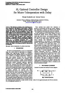
Proposed energy harvester system
high voltage operation of the CC (tens of volts). The circuit is designed in high-voltage 0.35 µm CMOS technology of AustriaMicrosystems. I. P ROPOSED VEH
SYSTEM
Fig. 3 shows the proposed IC assisting the CC. The designed circuit includes a switch controller and the switch itself with the auxiliary voltage level shifter. A. High-voltage switch The design of a switch between the charge pump and the flyback circuits presents a severe challenge, since it is a floating switch and it must operate with high voltage with respect to the ground. Its implementation is also restricted by low power consumption. As our theoretical study [2] revealed, in order to drive a flyback switch a complex control electronics is required, operating at standard voltage. It is possible to design a floating switch using a high-voltage PMOS device able to withstand high voltages (up to 50V for AMS 0.35µm HV) between its source and drain terminals. However its control voltage Vgs is limited by a low voltage set by the technology process (3.3V). The main issue is that Vgs is referenced to the floating high-voltage source terminal of HV-PMOS and, hence, its control is not straightforward and requires a voltage level shift [5]. The voltage level shifter is the most critical block of the system, mainly, because of the strict power limitations. There exist multiple architectures of level shifters. For our design the main criterion on the choice of circuit topology is the zero consumption in static mode. This requirement is fulfilled with the architecture using an analog memory to
store the state of the VDD-referenced transistor. Inspired from [6] the analog memory function is ensured with a dynamic RS flip-flop. The state of the flip-flop corresponds to the switch state and it is driven by low-voltage strobe signals on and off. The power dissipation is mostly limited to the triggering of the flip-flop to its new state. The sizing of switch itself is a trade-off between the input capacitance as well as conductive and leakage losses. While conducting few tens mA current. Indeed, PMOS device must have a large channel width and a small length in order to minimize the ”on” resistance Rdson. At the same time it should not be too large with intent to keep the input capacitance reasonably low regarding the high-speed performance as well as the power consumption. Theoretical study and simulation results provide us with an optimum transistor size: W=1000 µm, L=1 µm, where 1 µm is the minimum channel length for the used technology with highvoltage extension. Losses associated with the leakage current through a large channel transistor are about 500pA, that is approximately 15nW (for 30V) of power dissipated in static mode. B. Switch control block The purpose of the switch control block is the generation of switching events, specifically, strobe signals on/off. Another role of this block is the implementation of a periodic calibration phase allowing an ”auto-adaptation” to the external vibration varying in time and a re-initialization of the system. A control signal mode coordinates the operating conditions of the VEH: either calibration or harvesting phase. Since the CC is a high-voltage circuit and the controller is a standard voltage logic, voltage dividers and level shifter are included. Calibration mode: During the calibration, a single block of the controller system is enable - the generator of V1 and V2 . It is an analogue calculator sensing Vres and Vstore and performing the calculation of V1 and V2 following the formula (1). For further processing the outputs of the calculator are divided with external high resistors (up to 1GΩ) and are stored in relatively large on-chip capacitors (300pF). The division factor is around 12, since the maximum specified Vstore is limited to 30V and the maximum divided low-voltage is 2.5V. Harvesting mode: Harvesting mode is a normal longlasting operating phase. Controller implies the detection of two events necessary to open and close the switch. First event relates to the detection of the crossing of V2 point by Vstore . At this phase Vstore is divided with a factor 12 using another off-chip resistors and is compared with V2 , which was hold during the calibration. Divider and comparator are synchronized with a low-frequency (100Hz) clock clk harv. After the ”Vstore above V2 ” event detection, the on pulse is generated by a control logic and the switch activates a flyback circuit. At the same time the controller starts to
detect the crossing of V1 by Vstore . This phase lasts a very short time (few to tens µs) and, hence, requires a continuous time processing. The assisting voltage divider is composed of the series of 12 CMOS diodes due to division speed and power consumption. The operation of the V1 crossing detection block is controlled by a state machine. C. Power consumption The consumption of the proposed switch controller can be represented as a sum of power dissipated by low-voltage sub-circuits and by high-voltage counterparts. For the lowvoltage the most of energy is consumed by two comparators presented in the system (several hundreds of nA), while power consumption of few logic gates presented in the system can be neglected. Sub-circuits consuming energy from the high-voltage source are resistive and diode dividers, as well as a voltage level shifter with a flyback switch. Voltage dividers made with high-nominal resistors conduct a relatively low current (few to tens nA) during active phase, and they present maximum of 90pA of leakage current through NMOS transistors that act as switches. Diode-made voltage divider consumes few µA current but for a short duration of time (during a flyback phase), whereas it’s leakage current in ”off state” is represented by about 130 pA (for 30V). The voltage level shifter conduct 3mA current during two strobe signals (each lasts ≈50ns), and the leakage current mostly related to a large channel HV switch is 500pA for 30V. II. S IMULATION
RESULTS
The overall harvester system was modeled using highvoltage 0.35 µm AMS transistor models as well as the behavioral transducer model [1] which uses the parameters of the realistic transducer/resonator device presented in [3]. The external vibration frequency is around 250 Hz, the external acceleration amplitude is 1g. The initial voltage on Cres is 10V. Fig. 4(a) presents the transistor-level simulation results for the VEH operation during 50 seconds. The duration of the mode pulse (when calibration phase must be active) is 100ms and it repeats every 2 seconds (only for simulation purposes, in practice it should be tens seconds). Accordingly to the plot the voltage Vres increases continuously with time that corresponds to the accumulation of the converted energy. Fig. 4(b) is focused on the operation during calibration mode (in the middle) and the harvesting modes before and after update of V1 and V2 . During harvesting modes the divided voltage (Vst−div−s ) evaluates between V2 and V1 parameters, which are held constant. The division and comparison are processed every clk harv clock cycle. Fig. 4(c) is a zoom on the flyback phase. It shows the detection of V1 by Vstore and the switch controlling. Initially, the SW gate voltage Vgpsw equals Vstore . The on pulse forces Vgpsw voltage to become Vstore −3V , turning on the flyback switch.
III. C ONCLUSION
(a) Harvester long-term simulation
In this paper we proposed a transistor-level circuit design for the asynchronous electrostatic VEH, implementing the adaptive behavior. IC architecture includes a power management control block and a high-voltage switch. The designed circuit corresponds to the ultra-low power consumption requirements (0.9 µW at 14V on Cres ), however, the net average power generated on Cres under the same voltage is around 1.1 µW, which is just slightly higher then the power consumption. This figure can be improved using an optimized capacitive transducer, which is not part of current work, and with the maximization of the voltage level on Cres . The design was validated by mixed VHDLAMS/SPICE simulations using the high-voltage 0.35µm CMOS process provided by AMS. The implementation of a hard prototype of this circuit is a subject of ongoing work. ACKNOWLEDGEMENT The work is funded by a French National Research Agency under grant ANR-08-SEGI-019. R EFERENCES [1] Galayko D et al., AMS modeling of controlled switch for design optimization of capacitive vibration energy harvester Proc. of IEEE International Behavioral Modeling and Simulation Conference, pp. 115–120, Saint Jos´e, CA, 2007.
(b) Zoom on calibration mode
[2] A. Dudka et al., VHDL-AMS modeling of adaptive electrostatic harvester of vibration energy with dual-output DC-DC converter, Proc. of IEEE International Behavioral Modeling and Simulation Conference, pp. 13–18, Saint Jos´e, CA, 2009. [3] P. Basset et al., A batch-fabricated and electret-free silicon electrostatic vibration energy harvester, Journal of Micromechanics and Microengineering, 19:12pp., 2009. [4] P. Mitcheson et al., Architectures for Vibration-Driven Micropower Generators, Journal of Microelectromechanical Systems, 13(3):pp. 429–440, 2004.
(c) Zoom on flyback phase Figure 4.
Simulation results
[5] A. Kempitiya et al., Analysis and Optimization of Asynchronously Controlled Electrostatic Energy Harvesters IEEE Transactions on Industrial Electronics, VOL. 59, NO. 1, pp. 456–463, January 2012. [6] P. Basset, Conception, r´ealisation et test dun micro syst`eme de transport aliment´e a` distance PhD thesis, pp. 110–113, 2003. [7] A. R. Chandrakasan et al., Vibration-to-electric energy conversion IEEE Transaction On Very Large Scale Integration (VLSI) Systems, Vol. 9(1):64–76, February 2001.
It is important to notice that despite the floating Vstore , Vgpsw is kept constant during flyback, meaning that the switch is reliably closed. Voltage curves in the top present the V1 crossing detection phase: Vst−div−a outputted from the diode voltage divider repeats the behavior of Vstore , and as soon as Vst−div−a crosses the bottom line (V1 level), the off strobe is produced, opening SW.
[8] B. C. Yen et al., A Variable-Capacitance Vibration-to-Electric Energy Harvester IEEE TCAS, 53(2):288–295, February 2006. [9] E.O. Torres et al., A 0.7-um BiCMOS Electrostatic EnergyHarvesting System IC IEEE Journal of Solid States Circuits, vol. 45, n.2, pp. 483–496, February 2010.