May 10, 2016 - 4.9 Transformed circuits profiling, circuit b17. .... Modern EDA tools support TMR, as well as other basi
Design, Optimization, and Formal Verification of Circuit Fault-Tolerance Techniques Dmitry Burlyaev
To cite this version: Dmitry Burlyaev. Design, Optimization, and Formal Verification of Circuit Fault-Tolerance Techniques. Hardware Architecture [cs.AR]. Université Grenoble Alpes, 2015. English. .
HAL Id: tel-01253368 https://tel.archives-ouvertes.fr/tel-01253368v2 Submitted on 10 May 2016
HAL is a multi-disciplinary open access archive for the deposit and dissemination of scientific research documents, whether they are published or not. The documents may come from teaching and research institutions in France or abroad, or from public or private research centers.
L’archive ouverte pluridisciplinaire HAL, est destinée au dépôt et à la diffusion de documents scientifiques de niveau recherche, publiés ou non, émanant des établissements d’enseignement et de recherche français ou étrangers, des laboratoires publics ou privés.
THÈSE Pour obtenir le grade de
DOCTEUR DE L’UNIVERSITÉ DE GRENOBLE Spécialité : Informatique Arrêté ministériel : 2 juillet 2012
Présentée par
Dmitry Burlyaev Thèse dirigée par Pascal Fradet et codirigée par Alain Girault préparée au sein de l’INRIA et de l’École Doctorale Mathématiques, Sciences et Technologies de l’Information, Informatique
Design, Optimization, and Formal Verification of Circuit Fault-Tolerance Techniques Conception, optimisation, et vérification formelle de techniques de tolérance aux fautes pour circuits
Thèse soutenue publiquement le 26 Novembre 2015, devant le jury composé de :
Prof. Koen Claessen Chalmers University, Rapporteur
Dr. Arnaud Tisserand CNRS, Rapporteur
Prof. Florent de Dinechin INSA Lyon, Examinateur
Prof. Laurence Pierre Univ. Grenoble Alpes, Président
Dr. Pascal Fradet INRIA, Directeur de thèse
Dr. Alain Girault INRIA, Co-Directeur de thèse
Acknowledgements Je voudrais remercier mes directeurs, Pascal Fradet et Alain Girault, de leur aide, de leur patience, et du temps qu'ils ont consacr�e a me soutenir et m'encourager pendant ma these. Je vous suis reconnaissant pour tout, de la recherche de �nancement aux resultats scienti�ques aboutis. I also express gratitude to Vagelis, Sophie, Yoann, Gregor, Gideon, Peter, Helen, Christophe, Jean-Bernard, Adnan, Quentin, Willy and many many others. Our discussions helped me to be more fault-tolerant :) Îòäåëüíóþ áëàãîäàðíîñòü õî÷ó âûðàçèòü ìîèì ðîäèòåëÿì çà èõ êàæäîäíåâíóþ ïîääåðæêó. Áåç Âàøèõ ñîâåòîâ ýòà ðàáîòà íèêîãäà áû íå áûëà âûïîëíåíà.
Contents List of Figures
ii
List of Tables
iv
Glossary
vii
1 Introduction 1.1 Problems and Contributions . . . . . . . . . . . . . . . . . . . . . . . . . . . . 1.2 Outline . . . . . . . . . . . . . . . . . . . . . . . . . . . . . . . . . . . . . . .
1 2 4
2 Circuits Fault-Tolerance and Formal Methods 2.1 Circuits Fault Tolerance . . . . . . . . . . . . . . 2.1.1 Historical Roots of Fault-Tolerance . . . . 2.1.2 Taxonomy of Faults . . . . . . . . . . . . 2.1.3 Conventional Fault-Tolerance Techniques 2.2 Formal Methods in Circuit Design . . . . . . . . 2.2.1 Model Checking . . . . . . . . . . . . . . 2.2.2 Theorem Proving . . . . . . . . . . . . . . 2.3 Conclusion . . . . . . . . . . . . . . . . . . . . .
. . . . . . . .
. . . . . . . .
. . . . . . . .
. . . . . . . .
. . . . . . . .
. . . . . . . .
. . . . . . . .
. . . . . . . .
. . . . . . . .
. . . . . . . .
. . . . . . . .
. . . . . . . .
. . . . . . . .
. . . . . . . .
. . . . . . . .
. . . . . . . .
5 5 6 6 10 21 22 27 34
3 Verification-based Voter Minimization 3.1 Approach overview . . . . . . . . . . . 3.2 Syntactic Analysis . . . . . . . . . . . 3.3 Semantic Analysis . . . . . . . . . . . 3.3.1 The precise logic domain D1 . 3.3.2 Semantic analysis with D1 . . . 3.3.3 More Abstract Logic Domains 3.4 Inputs Specification . . . . . . . . . . 3.5 Outputs Specification . . . . . . . . . 3.6 Generalization to SETs . . . . . . . . 3.6.1 Precise modeling of SETs . . . 3.6.2 Safe SET over-approximation . 3.7 Experimental results . . . . . . . . . . 3.8 Related work . . . . . . . . . . . . . . 3.9 Conclusion . . . . . . . . . . . . . . .
. . . . . . . . . . . . . .
. . . . . . . . . . . . . .
. . . . . . . . . . . . . .
. . . . . . . . . . . . . .
. . . . . . . . . . . . . .
. . . . . . . . . . . . . .
. . . . . . . . . . . . . .
. . . . . . . . . . . . . .
. . . . . . . . . . . . . .
. . . . . . . . . . . . . .
. . . . . . . . . . . . . .
. . . . . . . . . . . . . .
. . . . . . . . . . . . . .
. . . . . . . . . . . . . .
. . . . . . . . . . . . . .
. . . . . . . . . . . . . .
. . . . . . . . . . . . . .
. . . . . . . . . . . . . .
35 35 36 37 37 37 39 41 42 44 45 46 47 52 53
4 Time-Redundancy Circuit Transformations 4.1 Basic notations and approach . . . . . . . . . . 4.2 Triple-Time Redundancy . . . . . . . . . . . . . 4.2.1 Principle of Triple-Time Redundancy . 4.2.2 TTR Memory Blocks . . . . . . . . . . . 4.2.3 TTR Control Block . . . . . . . . . . . 4.2.4 Fault-Tolerance Guarantees . . . . . . . 4.2.5 TTR Voting Mechanisms Minimization
. . . . . . .
. . . . . . .
. . . . . . .
. . . . . . .
. . . . . . .
. . . . . . .
. . . . . . .
. . . . . . .
. . . . . . .
. . . . . . .
. . . . . . .
. . . . . . .
. . . . . . .
. . . . . . .
. . . . . . .
. . . . . . .
. . . . . . .
55 56 58 58 59 61 62 63
. . . . . . . . . . . . . .
. . . . . . . . . . . . . .
. . . . . . . . . . . . . .
. . . . . . . . . . . . . .
ii
Contents
4.3
4.4
4.5
4.2.6 Experimental results . . . . . . . . . . . . . . . . . Dynamic Time Redundancy . . . . . . . . . . . . . . . . . 4.3.1 Principle of Dynamic Time Redundancy . . . . . . 4.3.2 Dynamic Triple-Time Redundancy . . . . . . . . . 4.3.3 Dynamic Double-Time Redundancy . . . . . . . . 4.3.4 Experimental results . . . . . . . . . . . . . . . . . Double-Time Redundancy with Checkpointing . . . . . . 4.4.1 Principle of Time Redundancy with Checkpointing 4.4.2 DTR Memory Blocks . . . . . . . . . . . . . . . . 4.4.3 DTR Input Buffers . . . . . . . . . . . . . . . . . . 4.4.4 DTR Output Buffers . . . . . . . . . . . . . . . . . 4.4.5 DTR Control Block . . . . . . . . . . . . . . . . . 4.4.6 Normal Execution Mode . . . . . . . . . . . . . . . 4.4.7 Recovery Execution Mode . . . . . . . . . . . . . . 4.4.8 Fault Tolerance Guarantees . . . . . . . . . . . . . 4.4.9 Experimental results . . . . . . . . . . . . . . . . . Conclusion . . . . . . . . . . . . . . . . . . . . . . . . . .
. . . . . . . . . . . . . . . . .
. . . . . . . . . . . . . . . . .
5 Formal proof of the DTR Transformation 5.1 Circuit Description Language . . . . . . . . . . . . . . . . . . 5.1.1 Syntax of lddl . . . . . . . . . . . . . . . . . . . . . . 5.1.2 Semantics of lddl . . . . . . . . . . . . . . . . . . . . 5.2 Specification of Fault Models . . . . . . . . . . . . . . . . . . 5.3 Overview of Correctness Proofs . . . . . . . . . . . . . . . . . 5.3.1 Transformation . . . . . . . . . . . . . . . . . . . . . . 5.3.2 Relations between the source and transformed circuits 5.3.3 Key Properties and Proofs . . . . . . . . . . . . . . . . 5.3.4 Practical issues . . . . . . . . . . . . . . . . . . . . . . 5.4 Correctness Proof of the DTR Transformation . . . . . . . . . 5.4.1 Formalization of DTR . . . . . . . . . . . . . . . . . . 5.4.2 Relations between source and transformed circuits . . 5.4.3 Main theorem . . . . . . . . . . . . . . . . . . . . . . . 5.4.4 Execution of a DTR circuit . . . . . . . . . . . . . . . 5.4.5 Lemmas on DTR components . . . . . . . . . . . . . . 5.5 Conclusion . . . . . . . . . . . . . . . . . . . . . . . . . . . .
. . . . . . . . . . . . . . . . . . . . . . . . . . . . . . . . .
. . . . . . . . . . . . . . . . . . . . . . . . . . . . . . . . .
. . . . . . . . . . . . . . . . . . . . . . . . . . . . . . . . .
. . . . . . . . . . . . . . . . . . . . . . . . . . . . . . . . .
. . . . . . . . . . . . . . . . . . . . . . . . . . . . . . . . .
. . . . . . . . . . . . . . . . . . . . . . . . . . . . . . . . .
. . . . . . . . . . . . . . . . . . . . . . . . . . . . . . . . .
. . . . . . . . . . . . . . . . . . . . . . . . . . . . . . . . .
. . . . . . . . . . . . . . . . .
63 66 67 70 78 81 83 84 86 87 87 89 90 91 93 96 98
. . . . . . . . . . . . . . . .
101 101 102 104 105 107 107 108 109 110 111 111 115 118 119 124 127
6 Conclusions 129 6.1 Summary . . . . . . . . . . . . . . . . . . . . . . . . . . . . . . . . . . . . . . 129 6.2 Future Work . . . . . . . . . . . . . . . . . . . . . . . . . . . . . . . . . . . . 130 Bibliography
133
List of Figures 2.1 2.2 2.3 2.4 2.5 2.6 2.7 2.8 2.9 2.10 2.11 2.12 2.13 2.14
Predicted number of bit-flips vs the number of observed bit-flips [1]. . . . . . Measured error rates dependency from supply voltage [2] . . . . . . . . . . . . TMR scheme proposed by von Neumann. . . . . . . . . . . . . . . . . . . . . TMR with only cells triplication for SEU masking. . . . . . . . . . . . . . . . Full TMR with a triplicated voter. . . . . . . . . . . . . . . . . . . . . . . . . Circuit realization of inter-clock time-redundant technique [3]. . . . . . . . . . Razor flip-flop for a pipeline stage [2]. . . . . . . . . . . . . . . . . . . . . . . Voting element for a time-multiplexed circuit [4]. . . . . . . . . . . . . . . . . Memory storage with ECC protection [5]. . . . . . . . . . . . . . . . . . . . . Three examples of state encoding for the FSM with 5 states. . . . . . . . . . Circuit with a majority voter. . . . . . . . . . . . . . . . . . . . . . . . . . . . Representations of the Boolean function fd (i, a, b, c) = (a ∧ b) ∨ (b ∧ c) ∨ (c ∧ a). A parametric OR-chain orN. . . . . . . . . . . . . . . . . . . . . . . . . . . . . Two abstraction levels of the processor AAMP5 operations [6]. . . . . . . . .
9 10 12 13 13 14 15 16 18 20 24 25 29 32
3.1 3.2 3.3 3.4 3.5
Input interface as an NBA (a) and its deterministic version (b) Original circuit with the surrounding interface circuit. . . . . . Combinational cones for SET modeling. . . . . . . . . . . . . . Logic Domain Comparison: Reachable State Space Size. . . . . Logic Domain Comparison: Size Ratio of RSS. . . . . . . . . .
. . . . .
42 43 46 50 51
4.1 4.2 4.3 4.4 4.5 4.6 4.7 4.8 4.9 4.10
Digital Circuit before the transformation. . . . . . . . . . . . . . . . . . . . . General scheme of a time-redundant circuit. . . . . . . . . . . . . . . . . . . . Transformed circuit for TTR. . . . . . . . . . . . . . . . . . . . . . . . . . . . TTR memory block without voting. . . . . . . . . . . . . . . . . . . . . . . . TTR memory block with voting. . . . . . . . . . . . . . . . . . . . . . . . . . TTR control block FSM. . . . . . . . . . . . . . . . . . . . . . . . . . . . . . . Circuit size after transformation (largest circuits). . . . . . . . . . . . . . . . Circuit size after transformation (smallest circuits). . . . . . . . . . . . . . . . Transformed circuits profiling, circuit b17. . . . . . . . . . . . . . . . . . . . . Throughput ratio of TMR and TTR transformed circuits (sorted according to circuit size). . . . . . . . . . . . . . . . . . . . . . . . . . . . . . . . . . . . . . Result of the circuit transformation DyTRN . . . . . . . . . . . . . . . . . . . General memory block structure for DyTRN . . . . . . . . . . . . . . . . . . . Control block for the generic DyTRN transformed circuit . . . . . . . . . . . Memory block for DyTR3 . . . . . . . . . . . . . . . . . . . . . . . . . . . . . . VotA: voter with detection capability. . . . . . . . . . . . . . . . . . . . . . . Control block for DyTR3 . . . . . . . . . . . . . . . . . . . . . . . . . . . . . . Memory Block for DyTR2 . . . . . . . . . . . . . . . . . . . . . . . . . . . . . . Control block for DyTR2 . . . . . . . . . . . . . . . . . . . . . . . . . . . . . . Transformed circuits profiling (circuit b21 ). . . . . . . . . . . . . . . . . . . . Circuit size after transformation, big circuits (for all COM/SEQ > 8). . . . . Circuit size after transformation, small circuits (for all COM/SEQ < 8). . .
56 57 59 59 61 61 64 64 65
4.11 4.12 4.13 4.14 4.15 4.16 4.17 4.18 4.19 4.20 4.21
. . . . .
. . . . .
. . . . .
. . . . .
. . . . .
. . . . .
. . . . .
66 67 68 70 71 72 74 79 80 82 82 83
iv
List of Figures 4.22 4.23 4.24 4.25 4.26
Overview of the DTR transformation. . . . Transformed DTR circuit. . . . . . . . . . . DTR Memory Block. . . . . . . . . . . . . . DTR input buffer (pi primary input). . . . DTR Output Buffer (co is the output of the
. . . . . . . . . . . . . . . . . . . . . . . . . . . . . . . . . . . . . . . . . . . . . . . . combinational part).
. . . . .
. . . . .
. . . . .
. . . . .
. . . . .
. . . . .
. . . . .
84 85 86 87 88
?
4.27 FSM of the DTR control block: “=” denotes a guard, “=” an assignment and signals absent from an edge are set to 0. fi is a fail delayed on one cycle. . . 4.28 Circuit size after transformation (large circuits). . . . . . . . . . . . . . . . . 4.29 Circuit size after transformation (small circuits). . . . . . . . . . . . . . . . . 4.30 Transformed circuits profiling (for b17 ). . . . . . . . . . . . . . . . . . . . . . 4.31 Throughput ratio of TMR, and DTR transformed circuits (sorted according to circuit size). . . . . . . . . . . . . . . . . . . . . . . . . . . . . . . . . . . . 4.32 Transformations overheads for throughput and hardware, the circuit b21. . . . . . . . . . . . . . . . . . . . . . . . . . . red. . . . . . . . . .
89 96 97 97 98 99
5.1 5.2 5.3 5.4 5.5 5.6 5.7 5.8 5.9 5.10 5.11 5.12
lddl syntax. . . . . . . . . . . . . . . . . . . . . . . . . . . . . . . . . . x −C operator. . . . . . . . . . . . . . . . . . . . . . . . . . . . . . . . . Simple memory cell ( x −swap). . . . . . . . . . . . . . . . . . . . . . . . Multiplexer realization . . . . . . . . . . . . . . . . . . . . . . . . . . . . lddl semantics for a clock cycle. . . . . . . . . . . . . . . . . . . . . . . lddl semantics with SET (main rules). . . . . . . . . . . . . . . . . . . Execution of source and transformed circuits described by predicates. . The internal structure of mb(d, d0 , r, r0 , cir). . . . . . . . . . . . . . . . . dtr(C) transformation composition: the types of buses are marked with DTR circuit step reduction described by predicates. . . . . . . . . . . . DTR circuit stepg reduction from the state described by Dtrs0. . . . . . Internal structure of a memory cell with an enable input. . . . . . . . .
102 103 103 103 105 106 108 112 115 120 121 123
6.1
a) Sequential, b) parallel, and c) feedback circuit decomposition. . . . . . . . 131
List of Tables 2.1.3 Hamming code (7,4). . . . . . . . . . . . . . . . . . . . . . . . . . . . . . . . .
19
3.2.0 Voter Minimization, Syntactic Analysis Step. . . . . . . . . . . . 3.3.1 Operators for 4-value logic domain D1 . . . . . . . . . . . . . . . 3.3.3 Operators for 4-value logic domain D2 . . . . . . . . . . . . . . . 3.7.0 Voter Minimization, SEU model, Boolean domains D1 | D2 | D3 . 3.7.0 Voter Minimization, SET model, Boolean domains D1 | D2 | D3 . 3.7.0 Time and memory resources to calculate the RSS. . . . . . . . . 3.7.0 Frequency and area gain of optimized vs full TMR. . . . . . . . .
. . . . . . .
37 38 40 47 50 51 52
. . . . . . . . . . . . at . .
75 75 76 77 80 91
4.3.2 Switching process 1 7→ 2. . . . . . . . . . . . . . . . . . . . . . . 4.3.2 Switching process 1 7→ 3. . . . . . . . . . . . . . . . . . . . . . . 4.3.2 Switching process 3 7→ 1. . . . . . . . . . . . . . . . . . . . . . . 4.3.2 Recovery procedure - DyTR3 , mode 3. . . . . . . . . . . . . . . 4.3.3 Switching process 1 7→ 2 7→ 1; ‘?’ is a don’t care. . . . . . . . . 4.4.6 Recovery process in DTR circuits. . . . . . . . . . . . . . . . . 4.4.7 Recovery Process: Input/Output Buffers Reaction for an Error cycle i. . . . . . . . . . . . . . . . . . . . . . . . . . . . . . . . .
. . . . . . .
. . . . . . .
. . . . . . .
. . . . . . .
. . . . . . .
. . . . . . . . . . . . . . . . . . . . . . . . . . . . . . . . . . . . Detection . . . . . .
. . . . . . .
93
5.4.4 Cases of glitched signal (introduced by stepg) and the resulting state corruptions.122
Glossary ALU Arithmetic Logic Unit. ASIC Application-Specific Integrated Circuit. BDD Binary-Decision Diagram. CIC Calculus of Inductive Constructions. CTL Computation Tree Logic. DMR Double Modular Redundancy. DTR Double-Time Redundant Transformation. ECC Error-Correcting Code. EDA Electronic Design Automation. ESA European Space Agency. FF flip-flop. FPGA Field-Programmable Gate Array. FSM Finite State Machine. HDL Hardware Description Language. IC Integrated Circuit. ITP Interactive Theorem Prover. LTL Linear Temporal Logic. MBU Multiple-Bit Upset. MVFS Minimum Vertex Feedback Set. RSS Reachable State Space. RTL Register-Transfer Level. SAA South Atlantic Anomaly. SED Single Event Disturb. SEFI Single-Event Functional Interrupt.
viii SEGR Single Event Gate Rupture. SEL Single-Event Latchup. SER Soft-Error Rate. SET Single-Event Transient. SEU Single-Event Upset. SHE Single Hard Error. STMR Selective Triple-Modular Redundancy. TMR Triple-Modular Redundancy. TTR Triple-Time Redundant Transformation. VLSI Very-Large-Scale Integration.
Glossary
Chapter 1
Introduction • “In 2008, a Quantas Airbus A330-303 pitched downward twice in rapid succession, diving first 650 feet and then 400 feet. ... The cause has been traced to errors in an on-board computer suspected to have been induced by cosmic rays.” [7] • “Canadian-based St. Jude Medical issued an advisory to doctors in 2005, warning that single bit-flips in the memory of its implantable cardiac defibrillators could cause excessive drain on the unit’s battery.” [8] This list could be continued by other examples of drastic consequences of fault occurrences. Proper circuit functionality even under perturbations and faults has been always crucial in aerospace, defense, medical, and nuclear applications. Circuit tolerance towards transient faults (non-destructive, non-permanent) is an important research topic and an unavoidable characteristic of any circuit used in safety critical applications. Common sources of faults are natural radiation, such as neutrons of cosmic rays and alpha particles of packing or solder materials, capacitive coupling, electromagnetic interference, etc [7, 9]. Nowadays, technology shrinking and voltage scaling increase electronics susceptibility and the risk of fault occurrences. Circuit engineers use fault-tolerance techniques to mask or, at least, to detect faults. Regardless of the chosen technique, this step increases the level of complexity of the whole design. Commonly used simulation-based methodologies are not able to fully verify even the functional correctness due to the huge number of possible execution cases. The verification of fault-tolerance properties by checking all fault injection scenarios raises the order of complexity. Non-exhaustive manual checks or simulation-based techniques are error-prone and may miss a circuit corruption scenario that leads to the loss of the circuit functionality or to degraded quality of service. Since engineers need their implementations to be simple and correct, they mostly use Triple-Modular Redundancy (TMR), a technique that triplicates the circuit and introduces majority voters. Modern EDA tools support TMR, as well as other basic techniques such as Finite State Machine (FSM) encoding [10–12], through automatic circuit transformations. While there are other more elegant and optimized fault-tolerance techniques [13, 14], their functional correctness and fault-tolerance properties are often not guaranteed. Ensuring correctness of fault-tolerance techniques requires mathematically based techniques for the specification, development, and verification. Formalization of fault-models, circuit designs, and specifications gives a vast opportunity to create, to optimize, and to check the correctness of fault-tolerance techniques. Showing fault-tolerance properties w.r.t. the chosen fault-model eliminates all doubts about the circuit functionality under the faults whose occurrence and type are specified by the fault-model. Thanks to this formal verification, the overall probability of the system failure is purely the probability of faults occurring outside of the fault-model. There are many different formal methods to verify properties of systems or circuits. In this dissertation, we mainly use static symbolic analysis and theorem proving.
2
Chapter 1. Introduction
1.1
Problems and Contributions
Throughout the dissertation, we work with circuits described at the gate level (i.e., netlists of AND, OR, NOT gates plus flip-flops (FFs) – also called memory cells). This decision offers two main advantages: • gate-level netlists can be captured in an elementary language, which simplifies formal circuit representations (e.g., as a transition system) and correctness proofs; • it is easier to prevent synthesis tools from optimizing (undoing) our transformations at this late stage, as well as to integrate the circuit transformations in commercial logic synthesis tools that we use for benchmarking. We address three problems of circuit fault-tolerance: an optimization of a standard faulttolerance technique based on static analyses, the design of several new fault-tolerance techniques based on time redundancy, and the formal proof of their functional and fault-tolerance properties. Verification-based optimization of fault-tolerance techniques. Making a circuit fault-tolerant always leads to overheads in terms of performance and hardware resources. The circuit transformations for fault-tolerance usually do not take into account any peculiarities and functionality of the original circuit. Moreover, they do not take into account neither how the circuit is used nor what fault-tolerance properties are indeed needed. There is significant room for optimizations if we take into account the circuit original design, its utilization, and the expected fault rate. For instance, if it is known that faults are less frequent than one fault per K clock cycles, it may be possible to suppress some fault-tolerance mechanisms which would be overkill for the required fault-tolerance property. A crucial point is that, while optimizing a fault-tolerant design, we have to be sure that the fault-tolerance and functional properties are not violated. The guarantees can be given if the design, its properties, the fault-model, and the optimization procedure are formally defined and taken into account. Our first step is to consider error-masking mechanisms in fault-tolerance techniques as an object of optimization and to develop a verification-based approach to suppress them. For instance in TMR, error-masking mechanisms are majority voters introduced after triplicated memory cells. We propose an approach to minimize the number of voters in TMR with guarantees that, after this optimization, the circuit is still tolerant w.r.t. the given faultmodel [15]. While the final goal is to suppress as many voters as possible, the developed methodology clarifies how to take into account the original circuit functionality and the circuit typical use. Many circuits have native error-masking capabilities due to the structure of its combinational part, embedded FSMs, or due to the way the circuit is commonly used and communicates with the surrounding device. The developed methods take these native error-masking properties into account and identify useless voters that can be suppressed without violation of the fault-tolerance properties. We demonstrate how to consider large class of fault-models of the form “at most one bit-flip or one wire-glitch every K clock cycle”, where K is a chosen parameter. The formalization of a circuit, its typical utilization, the fault-model as well as optimization steps using static analysis distinguish this work from [16–18] where probabilistic simulation-based approaches are followed. In our case, the circuit fault-tolerance is guaranteed w.r.t. its fault-model before and after optimizations.
1.1. Problems and Contributions
3
Universal time-redundant techniques as circuit transformations. TMR has multiple advantages as a throughput comparable to the original one and unchanged input/ouput interfaces. However, the triple permanent hardware overhead is often prohibitive. Timeredundant techniques could produce circuits several times smaller than their TMR counterparts but would obviously reduce the circuit performance. However, many safety-critical applications may accept the reduced throughput to obtain strong fault-tolerance guarantees, small hardware overhead, and flexibility. Unfortunately, to the best of our knowledge, there is no simple and trusted alternative to TMR among time-redundant fault-tolerance techniques. We propose a circuit transformation, called Triple-Time Redundant Transformation (TTR), that automatically makes any sequential circuit triple-time redundant and capable to mask any effect of a glitch occurrence. We explain that TTR circuits can also be optimized with the aforementioned voter minimization analysis because the error-masking analysis stays the same regardless of redundancy type (hardware redundancy in TMR and time redundancy in TTR). Second, we introduce the notion of dynamic time redundancy, a circuit property that allows it to dynamically change the level of redundancy without interrupting the computation [19]. We also propose a family of circuit transformations that implements this property. The transformed circuit may dynamically adapt the throughput/fault-tolerance trade-off by changing its redundancy level. Therefore, time-redundancy can be used only in critical situations (e.g., above the South Atlantic Anomaly (SAA) or Earth poles where the radiation level increases), during the processing of crucial data (e.g., encryption of selected data), or critical processes (e.g., a satellite computer reboot). When hardware size is limited and fault-tolerance is only occasionally needed, the proposed scheme is a better choice than TMR, which incurs a constant hardware area overhead, or than TTR which has a constant throughput cost. Third, we merge the proposed principle of dynamic time redundancy and a checkpointingrollback mechanism to obtain the Double-Time Redundant Transformation (DTR). DTR is capable to recover from any transient fault consequences with only a double redundancy and without disturbing the input/output streams [20]. The recovery process remains transparent for the surrounding circuit. While TTR has similar error-masking properties, it introduces a higher throughput overhead than DTR. It allows us to state that DTR is an interesting logic-level time-redundant alternative to TMR in applications where a reduced throughput is tolerable. All presented circuit transformations are technologically independent, do not require any specific hardware support, and are applicable to any circuit. Moreover, their fault-tolerance properties are formally provable which is crucial for safety-critical systems. Formal proof of circuit transformation correctness. Universal fault-tolerance techniques have to be applicable to any circuit and, thus, are defined independently from a particular circuit implementation. The circuit transformations to implement these techniques are defined on the syntax of a Hardware Description Language (HDL). The functional correctness of the transformation as well as its fault-tolerance properties have to be assured independently from the circuit the transformation is applied to. The fault-tolerance properties rely on the notion of fault model that is formalized in the semantics of HDL. However, modern hardware description languages, like Verilog or VHDL, do not have formal semantics. We propose a language-based approach to formally certify the functional and fault-
4
Chapter 1. Introduction
tolerance properties of circuit transformations using the Coq proof assistant [21]. We define the syntax and semantics of a simple gate-level functional HDL, called lddl, to describe circuits. We focus on the DTR transformation whose complexity made it necessary to provide a formal proof for full assurance of its correctness. While we relied on many manual checks to design all presented transformations, only Coq allowed us to get complete correctness guarantees. The DTR transformation is defined as a recursive function on the lddl syntax. The fault-model of the form “at most one transient fault every K cycle” is formalized in the language semantics. Proofs rely mainly on relating the execution of the source circuit without faults to the execution of the DTR circuit w.r.t. the fault-model. To the best of our knowledge, our work is the first to certify automatic circuit transformations for fault-tolerance.
1.2
Outline
The thesis is structured as follows: Chapter 2 starts by presenting background information on circuit fault tolerance (Section 2.1). It provides details about faults, their characteristics, and the techniques to make circuits fault-tolerant. Later (Section 2.2), we give an overview of the main approaches in formal hardware verification including model checking, symbolic simulation, and theorem proving. We focus on these formal techniques and their applications because they are used throughout the dissertation. The rest of the work is structured according to the problems-contributions list presented above. Chapter 3 presents our formal solution to minimize the number of voters in TMR sequential circuits, keeping the required fault-tolerance properties. Chapter 4 starts with the presentation of the TTR circuit transformation explaining the main principle of any timeredundant transformation proposed in this dissertation. Then, it presents the idea of dynamic time redundancy and the corresponding circuit transformations with their properties. Chapter 4 ends by proposing the DTR transformation capable to mask any transient fault which makes it an interesting alternative to hardware redundant solutions. In Chapter 5, we present a language-based solution to certify circuit transformations for fault-tolerance in digital circuits. We focus on the details of the DTR correctness proof in the Coq proof assistant. Finally, the thesis is summarized in Chapter 6, where contributions and future work perspectives are discussed.
Chapter 2
Circuits Fault-Tolerance and Formal Methods
Fault-tolerance has become a design characteristic of circuits as important as performance and power consumption [22]. Proper circuit functionality even under perturbations and faults has been always a crucial characteristic for safety-critical systems (e.g., aerospace, defense, and nuclear plants applications). Nowadays, circuit fault-tolerance is a research topic for many more devices due to the increased fault sensitivity caused by shrinking transistor sizes. The integration of fault-tolerance techniques represents a new design step to already convoluted functional circuit design. These techniques can be implemented manually and the final system properties can be checked by simulations. However, as the design complexity increases, an even smaller percentage of circuit behavior scenarios can be covered by simulation methods. Consequently, it does not provide confidence in the design correctness, which is unacceptable for safety-critical applications. It is even a more challenging task to cover all possible system behaviors under faults due to the high number of fault injection cases. Formal hardware verification methods attempt to overcome the weakness of non-exhaustive simulation-based methods by proving the correspondence between the desired properties expressed in the specification and the implemented circuit design. Overall, formal methods are mathematically rigorous techniques for the specification, design, analysis, and verification of systems. Section 2.1 provides a brief background on the topic of fault tolerance and its terminology. Section 2.1.1 explains the roots of the research domain and Section 2.1.2 provides details about faults, their classification, characteristics, and ways of modelling them. The fundamental principles and modern techniques to tolerate faults are presented in Section 2.1.3. We give an overview of the main approaches in formal hardware verification in Section 2.2: model checking and symbolic simulation in Section 2.2.1; theorem proving in Section 2.2.2. We outline the underlying theory behind these approaches and illustrate them on simple examples. Section 2.3 concludes this chapter by explaining the research directions and motivations of the dissertation.
2.1
Circuits Fault Tolerance
Fault tolerance is the ability of a system to operate according to its specification in the presence of faults [23]. The term fault is used to identify the initiating physical event whereas the term error identifies the undesired system state. The way how we model faults and their consequences is defined by a fault-model. A failure is an event that occurs when the delivered service deviates from correct one [23]. In these terms, fault tolerance is the ability to avoid failures in the presence of faults and, thus, to deliver the specified service and correct results. The
6
Chapter 2. Circuits Fault-Tolerance and Formal Methods
correctness of a computational process is defined by the absence of incorrect outputs. The correctness of the output result stays the most important characteristic of any computation performed by a system. The only reason why a correctly designed system can return incorrect results and violate its specification is the existence of physical faults. They can be often avoided or their risk can be minimized by a range of measures, such as the use of highly reliable materials during the device manufacturing, the increase of voltage and frequency margins, etc. These measures form the fault-avoidance technique category [23]. Unfortunately, these techniques either cannot fully guarantee the absence of faults or they are not cost effective. Nevertheless, the computational correctness under specific fault-models can be provided using fault-tolerance techniques [24]. The large range of fault-tolerance techniques has been developed at different abstraction levels of system design but all of them can be classified according to the redundancy type they rely on: hardware, time, or information redundancy. The most common techniques are discussed in Section 2.1.3. The main principles and fault-tolerance techniques appeared with the first computers. We introduce fault tolerance from its historical retrospective in Section 2.1.1. Section 2.1.2 explains the difference between different fault types showing the main peculiarities of softerrors. The vast research on fault-tolerance techniques is presented in Section 2.1.3 where the three fundamental redundancy types are introduced.
2.1.1
Historical Roots of Fault-Tolerance
The lack of reliability in early computers of the 1940s-1950s [25, 26] gave rise to the faulttolerance domain. Unreliable hardware components were the main issue. For instance, ENIAC [27] had only 54% of correct computations due to reliability-related issues. The EDAVAC computer of 1949 was the first one with an error-detection implemented with duplicated Arithmetic Logic Units (ALUs) [26]. Error-Correcting Codes (ECCs) for memory scrubbing and parity checking have been integrated later in 1951 in Univac I architecture [28] as well as in IBM 650 which used multiple redundant components. New challenges for fault-tolerance research came when computers appeared in aerospace, military, and other safety critical applications in the 1960s [29]. The space programs and artificial satellites needed fault-tolerance techniques for electronics protection from harsh radiation environment. Hardware redundancy was extensively used to avoid potential costs of mission failures [30, 31]. Since the 1980s, the fourth computer generation gave birth to Very-Large-Scale Integration (VLSI) and the corresponding technological trend of feature size and power consumption minimization [32]. It leaded to an increased risk of soft errors in logic components [33,34]. If fault-tolerance techniques against soft errors could be found before only in special-purpose expensive computers (e.g., controlling aerospace missions), from now on, the increasing integration has raised the fault probability in any general-purpose system [35]. As a result, fault-tolerance techniques are nowadays used in a wide range of computer systems, from personal computers and corporate servers to embedded systems in automotive, health, railway, energy, and production industries.
2.1.2
Taxonomy of Faults
Avizienis [23] classified all kind of existing faults in several subcategories (software or hardware, natural or human-made, etc). In the context of circuit fault tolerance, we consider the
2.1. Circuits Fault Tolerance
7
subcategory of natural operational hardware faults. Natural faults, by definition, are caused by natural phenomena without human participation (versus human-made faults). Operational faults occur during the service delivery of a circuit. Thus, the development faults, caused by design mistakes, are commonly out of the scope of the fault-tolerance research domain. Faults can be classified according to their source: internal and external ones. For instance, noise-related faults [32] or cross talks between wires can be considered as internal because their original cause is electrical disturbances inside the circuit. On the other hand, the sources of external faults exist outside of the system such as external electromagnetic fields, natural radiation in the form of neutrons of cosmic rays [36] and alpha particles emitted by packing or solder materials [37–40]. Moreover, faults can be further divided according to their persistence: they are either permanent or transient. A permanent fault is a hardware damage that is continuous in time (e.g., a wire break). Transient faults have non-destructive and non-permanent hardware effects. They manifest themselves as soft-errors and they can be represented as some information loss or a system incorrect state. Integrated Circuits (ICs) are now increasingly susceptible to transient faults [7, 9]. A typical representative of natural operational hardware faults are faults caused by radiation. The increased risk of these faults results from the continuous shrinking of transistor size that makes components more sensitive to radiation [9]. Having been an object of attention in space and medical industries for many years [41], these faults represent a danger for all circuits manufactured at 90nm and smaller [22]. Space-based radiation comprises atomic particles that have been spread by stellar events within the solar system or beyond it [42]. The statistical correlation between radiationinduced faults in satellite electronics and solar activities was revealed by the Hiten satellite mission [43]. Earth’s magnetosphere traps, slows, or deflects electrons, protons, and heavy ions (isotopes of atom from helium to uranium) emitted during solar events such as solar flares and mass coronal ejection, which reduces the rate and the impact of radiation particles on electronic devices used in the atmosphere. However, there is a region, called South Atlantic Anomaly (SAA), where the magnetic field extends downwards the Earth. High concentration of protons is observed in this region at lower altitudes, which constitutes a danger for satellites and planes. But even on the ground radiation-related faults are common. Electronics materials contain high-density atoms due to their impurities. These atoms emit alpha particles that inject charges leading to soft errors [44]. Package materials are also a source of alpha particle emission and should be chosen carefully for safety-critical applications. Other sources of faults include energetic neutrons: if a neutron is captured by the nucleus of an atom in an electronic device, an alpha particle and oxygen nuclei are produced. There is a 0.95 probability that this will cause a soft error [45]. Since neutron flux is a function of altitude, neutron-based faults are more frequent for aerospace applications. For instance, computers at mountaintops experience over 10 times more soft error than at sea level [46], and electronics devices in airplanes 300 times more. All radiation-related faults have the same physical nature, which consists in the material ionization caused by a high energetic particle hit. In particular, when a charged particle is passing through an electronic device, it ionizes the material along its path. Because of such ionization, free carriers are created around the particle track. In interaction with the internal electric field of the device, it may result in an electrical pulse or a glitch that disrupts normal
8
Chapter 2. Circuits Fault-Tolerance and Formal Methods
device operation. Such an effect, called a soft error, does not cause any permanent damage of the hardware but leads to a wrong system state. Since both supply voltage levels VDD and the circuit nodes capacitance C are reducing with newer technologies, the charge stored on a circuit node (Q = VDD xC) is decreasing. It reduces the required charge from a radiation particle to reverse the node value. As a result, the increasing sensitivity is observed in both memory cells and logic network. On the other hand, a large energy deposition by a passing particle can influence memory cells such that they loss their ability to change the state. Such permanent faults lead to hardware lasting rupture: Single-Event Latchup (SEL), Single Hard Error (SHE), Single Event Gate Rupture (SEGR), etc. SEL is a type of short circuit that may cause the loss of device functionality. High current may cause permanent device damage if the device is not power cycled as soon as high power consumption is detected. SHE leads to a stuck bit in a memory device. The output of such bit is stuck at logic 0 or 1, regardless of the input. We focus in this dissertation on transient faults. The effects of all single transient faults can be grouped into two sub-categories, SEU and SET: Single-Event Upset (SEU) is the disturbance of a memory cell that leads to the change of its state, i.e., a bit-flip. SEUs can be caused by a direct particle hit. A radiation particle creates a transient pulse that can be captured by the asynchronous loop forming the memory cell and can change its state. Historically, SEUs in memory cells were the main contributors to the fault rate due the sensitivity of memory elements [47]. Single-Event Transient (SET) is a transient current in a combinational circuit induced by the passage of a particle. It may propagate through the combinational logic depending on its electrical characteristics and if not logically masked by circuit functionality. As a result, the outputs of the combinational circuit might be glitched and be incorrectly latched by memory cells. Since an SET may potentially lead to several bit-flips, SETs subsumes SEUs. SET-caused glitches are not attenuated because the logic transition time of gates is shorter than a typical glitch duration. Moreover, the increasing circuit clock frequencies increase the probability to latch a transient pulse. Nowadays, the combinatorial circuits are becoming as susceptible to faults as memory cells [48]. The classifications by NASA [49] and by ESA [50] also distinguish other transient faults. Some of them are given hereafter: Single Event Disturb (SED) : A momentary disturbance of the information stored in memory cells. It can manifest itself only when the information is incorrectly read out. The bits state remains correct. Single-Event Functional Interrupt (SEFI) : A condition where the device stops operating in its normal mode, and usually requires a power reset or other special sequence to resume normal operations. It is a special case of an SEU changing an internal control signal. Multiple-Bit Upset (MBU) : An event induced by a single energetic particle that causes multiple upsets or transients during its path through a device. The analysis of MBUs requires the knowledge about the circuit physical layout due to its spatial nature. Even if they have different characteristics and behavior, any single radiation transient fault can be modeled as either an SEU or an SET. For instance, the effect of an SED can be
2.1. Circuits Fault Tolerance
9
modelled as an SET on the output of a memory cell. The memory cell will keep its correct state but its output will be read incorrectly. A SEFI is just a special case of an SEU: the term Single-Event Functional Interrupt (SEFI) is usually used when internal circuit design is unknown but it is necessary to describe its corruption. In such cases, one may say: “A SEFI interrupted CPU normal execution”. The term SEU is more commonly used when a location of a bit-flip is known (e.g., a particular memory cell). An MBUs can be modelled as multiple SEUs [51]. 2.1.2.1
Fault Rate and Fault Model
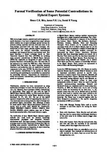
Even in environments with high levels of ionizing radiations (e.g., space, particle accelerators), transient faults happen rare relatively to clock periods of modern devices. Below, we provide several observations of the fault rates in different environmental conditions. The experiments of TIMA laboratory with 1 Gbit of SRAM memory at 130 nm technology have shown that 15 soft-errors have been observed during the flight Los Angeles-Paris (23/4/2009) [1]. Among them, there were 5 SEUs and 4 MBUs. It verified the precision of the developed prediction tool MUCSA. The dependence between the flight length and the number of bit-flips is presented in Figure 2.1.
Figure 2.1: Predicted number of bit-flips vs the number of observed bit-flips [1]. In other experiments in Peru at 3800m, 1 Gbit of SRAM at 90 nm and 130 nm experienced 37 bit-flips during 5 months: 10 SEUs and 9 MBUs [1]. Soft-Error Rate (SER) can be as small as 10−5 bit-upset/day for Vertex FPGAs [52] in terrestrial conditions. At geosynchronous Earth orbit altitudes, Lockheed Martin Commercial Space Systems observed 1.8x10⁻¹⁰ errors/bit/day in SRAM 0.25µm devices [53]. During solar maximum condition, SER raised to 1x10⁻⁹ errors/bit/day. MBUs constituted 4-10% of all faults. Microsemi Corporation [7] lists an extensive list which shows that the radiation-based soft-errors are widely observed and already leaded to incidents. Among others, let us cite: • “In 2008, a Quantas Airbus A330-303 pitched downward twice in rapid succession, diving first 650 feet and then 400 feet. The cause has been traced to errors in an
10
Chapter 2. Circuits Fault-Tolerance and Formal Methods on-board computer suspected to have been induced by cosmic rays.” • “Canadian-based St. Jude Medical issued an advisory to doctors in 2005, warning that SEUs to the memory of its implantable cardiac defibrillators could cause excessive drain on the unit’s battery.” The observed SER in defibrillators was 9.3x10⁻¹² upsets/bithour [8].
Due to low fault rates on Earth or even in open space, the most common fault-model is a single fault, e.g., an SEU or an SET. If we relate SER with the number of system clock cycles between two consecutive faults, then we can introduce fault models of the form “at most n bit-flips within K cycles”, denoted by SEU (n, K), and “at most n SETs within K cycles”, denoted by SET (n, K). Besides radiation-related faults, it is worth to mention the faults caused by signal metastability during aggressive voltage scaling [2]. Voltage scaling is a technique to reduce circuit energy demands, it decreases the voltage in the circuit to minimize its power consumption. Figure 2.2 illustrates the dependency between voltage and error rates for an 18x18-bit multiplier at 90MHz in Xilinx XC2V250-F456-5 FPGA. 100.00000000 Errordratedpercentaged(logdscale)
10.00000000 1.00000000 0.10000000 0.01000000 0.00100000 0.00010000 0.00001000 0.00000100
Onederrordeveryd~20dseconds
0.00000010 0.00000001 1.78 1.74 1.70 1.66 1.62 1.58 1.54 1.50 1.46 1.42 1.38 1.34 1.30 1.26 1.22 1.18 1.14 Supplydvoltage
Figure 2.2: Measured error rates dependency from supply voltage [2] As it is marked on the plot, when the voltage is 1.52 V, the error rate is one error per 20 seconds or per 1.8 billion operations. It corresponds to the fault model SET (1, 1.8x10⁹ ).
2.1.3
Conventional Fault-Tolerance Techniques
Any fault-tolerance technique is based on some sort of redundancy. There are three redundancy classes: Hardware or spatial redundancy. It adds additional hardware resources to simultaneously produce several copies of the same computational result for their further comparison (resp. voting) to detect (resp. to mask) soft-errors. For instance, a duplicated system is capable to detect an error occurrence by comparing the states of its two redundant modules. The triplicated design can mask an error by majority voting. Additional hardware introduces the corresponding cost in terms of physical space, power, etc, but it allows avoiding significant performance degradation because redundant computations are performed in parallel.
2.1. Circuits Fault Tolerance
11
Time or temporal redundancy. The redundant computations are performed sequentially multiple times re-using the same hardware resources. Thus, time redundancy trades-off performance for a low hardware cost. For instance, if a system re-computes its result twice for further comparison, it is capable to detect an error. If the computation is triplicated in time, the system can mask an error by voting on the redundant results. Information redundancy. It adds extra information (bits) to be used for detection/correction purposes. To operate with and use this information, e.g., parity bits, a system also needs additional hardware and/or time resources that encode/decode this extra data. Furthermore, there is an orthogonal classification of the redundancy types according to the system reaction upon error detection and the guarantees on the primary outputs correctness. In particular: Active redundancy relies on an error-detection with a subsequent appropriate system reaction. For example, the system performs a global reset after an error-detection in any of its redundant copies. Passive redundancy is based on fault-masking techniques to guarantee the correctness of the primary outputs. Any fault occurring in the system protected by passive redundancy does not change the system output behavior. Hybrid redundancy incorporates both active and passive types of redundancy. Since active redundancy does not guarantee the equivalence of output streams with and without fault occurrence, it is typically used in systems that can tolerate some temporal service quality degradation. As the European Space Agency (ESA) states: “In some applications it is sufficient to detect an error caused by an SEU and to flag the affected data as invalid or corrupted” [49]. The two observed classifications are orthogonal. There are systems where an error detection of active redundancy is realized through hardware duplication with comparison (hardware redundancy), error detection codes (information redundancy), or self-checking logic (time redundancy) [31]. The next three sections present hardware, time, and information redundancies in details. 2.1.3.1
Hardware Redundancy
The lectures by von Neumann given in Princeton University in 1952 [54] can be considered as the first theoretical work about hardware redundancy. He proposed and analyzed TripleModular Redundancy (TMR) that stays to be the most popular approach for error masking in safety-critical applications. TMR relies on three redundant copies of an original system receiving the same inputs. Majority voters are introduced at the primary triplicated outputs. If at least two of three redundant outputs return correct values, the voters return the correct result, therefore masking one possible error. TMR is able to detect one or two errors and to correct one. Double Modular Redundancy (DMR) represents the reduced version of TMR that has only two redundant modules and is only capable to detect one error. The generalized version of TMR, called N-modular redundancy, requires N redundant copies of a system to feed majority voters with N inputs. It can correct b N 2−1 c errors and detect (N − 1) errors. There are several versions of TMR that can be applied to circuits [12], in particular:
12
Chapter 2. Circuits Fault-Tolerance and Formal Methods 1. the whole circuit triplication with the insertion of a single majority voter at each primary output (as in the von Neumann’s original TMR); 2. only memory cells are triplicated with a single voter after each triplicated cell and each primary output; 3. the whole circuit triplication with a single voter after each triplicated memory cell and each triplicated primary output; 4. the whole circuit triplication with three voters after each triplicated memory cell and each triplicated primary output.
The first TMR version, depicted in Figure 2.3, is tolerant only to a single fault, temporal or permanent, occurring inside one of the redundant modules. When a fault occurs in a module, its state becomes corrupted and may stay erroneous forever if it does not have any additional error-masking mechanisms. This is why this scheme is tolerant only to a single internal fault of the modules. This TMR version may not be capable to tolerate a second fault occurring in a different module. If another fault occurs (even long after the first one) and corrupts the second module, the TMR structure would have two erroneous modules simultaneously and cannot guarantee anymore the correctness of primary outputs. Furthermore, if an SET corrupts an output voter, then the correctness of the output is not guaranteed. As a result, the first TMR modification is tolerant to the fault models (notations of Section 2.1.2.1): SEU (1, ∞) and SET (1, ∞), provided that faults do not occur at the output voters.
Module Input
Module Module
Figure 2.3: TMR scheme proposed by von Neumann. The second TMR version triplicates only memory cells introducing a single majority voter per each triplet, see Figure 2.4. This approach relies on the assumption that radiation effects cannot cause perturbations in a combinational circuit (which is not triplicated in this case). In other words, it protects only against SEUs. Indeed, an SET in the non-redundant combinational part could simultaneously corrupt three redundant memory cells and that error would not be masked after the voting on this triple. The second TMR version makes any circuit fault-tolerant to the fault model SEU (1, 2). If an SEU happened every clock cycle, then one redundant cell could be corrupted at the end of the cycle i and the next fault could corrupt its redundant copy at the beginning of the cycle i + 1. In this case, the majority voting that happens after the triplicated cells would produce an incorrect result because two of three redundant cells have a wrong value. The third version triplicates both the combinational and the sequential parts of the original circuit. Voters are inserted after each triplicated memory cell and each primary output but they are not triplicated. This scheme assumes that voters are fault-tolerant by
2.1. Circuits Fault Tolerance
13
comb.
Figure 2.4: TMR with only cells triplication for SEU masking. themselves. For instance, the voters could be radiation hardened and produced by a different technology than the rest of the circuit. This version can tolerate the fault models SEU (1, 2) or SET (1, 2) assuming no fault occurs at voters. Since the later fault-model subsumes the former one, we write just SET (1, 2). Again, if faults happen every cycle, this TMR protection is not capable to mask them for the same reason as in the previous case. The fourth TMR version works exactly as the third one but its voters are triplicated, see Figure 2.5. It tolerates the fault-model SET (1, 2) without assumptions on voters. This TMR version is often referred as “full TMR” since all original circuit components and voters are triplicated. The first TMR version can be considered as the fourth one where voters after all triplicated memory cells have been suppressed.
comb. comb. comb.
Figure 2.5: Full TMR with a triplicated voter. The second and the fourth TMR versions are well supported by the majority of existing Electronic Design Automation (EDA) synthesis tools like Xilinx XTMR tool [10, 55], BYU Los Alamos National Laboratory B-TMR [56], Synopsys Synplify Premier [11], and Mentor Graphics Precision Hi-Rel [12]. The inclusion of TMR can be also done manually directly in VHDL, as it has been done in the LEON SPARC ESA microprocessor [49]. Since hardware redundancy introduces a high hardware overhead, it is usually used only in high reliability/availability applications (e.g., for aerospace and nuclear applications). In-
14
Chapter 2. Circuits Fault-Tolerance and Formal Methods
terestingly, hardware redundancy (as any other redundancy type) can be applied at different design abstraction levels, from transistors to the whole system. The NASA shuttle used five-time redundant on-board computers, the primary flight computer of Boeing 777 is triplicated [57], four-time component-level redundancy has been implemented in PPDS computer of NASA Orbiting Astronomical Observatory satellite [58], triplicated CPUs are used in automotive applications [59]. 2.1.3.2
Time Redundancy
The basic principle of all time redundant techniques is data re-computation for further comparison/voting. The hardware overhead of time redundancy is significantly lower than that of hardware-redundancy because the same hardware is used to re-compute. On the other hand, the performance degradation often prohibits the use of this technique in applications demanding high throughout (e.g., real-time). We can distinguish time-redundant techniques based on the period P (or granularity) of the re-computation of redundant results. For example, techniques that produce redundant information within one clock cycle have the re-computation period P < 1. If a circuit recomputes its state after one cycle, then P = 1; and if it performs several times a multi-cycle computation, then P > 1. The period of recomputation is connected with the abstraction level where a fault-tolerance technique is introduced: lower the level, shorter the period can be reached. We start the overview of time-redundant techniques with the low-level ones that have P < 1. Nicolaidis et al. [3, 60] presented a time-redundant IC transformation at the transistor level. Since an SET manifests itself for a limited duration of time in a combinational circuit, the circuit timing properties should be adjusted so that the correct values are present on the circuit outputs for a time duration greater than the duration of the transient fault. Consequently, if the signal is latched at three different instances of time with guarantees that a glitch can be latched only once, the majority voter after the memory cells is able to filter out the corrupted latched value. The implementation of such mechanism is presented in Figure 2.6.
Combinational Circuit Clk1
Clk1+2δ
Latch 1
Latch 3
Latch 2
Clk1+δ
Voter Clk
Output Latch
Figure 2.6: Circuit realization of inter-clock time-redundant technique [3]. The three latching edges of the three clock lines are shifted relatively to each other on δ, which is chosen based on the targeted transient pulse duration. This construction guarantees that a glitch in the combinational circuit cannot affect more than one latch, which assures the output correctness of the output latch. This time-redundant technique has an area
2.1. Circuits Fault Tolerance
15
overhead of 15 − 23% and 10 − 15% depending on the SET pulse duration, 0.45ns and 0.15ns respectively. The performance degradation is 20 − 50% for 0.45ns and 10 − 22% for 0.15ns glitches. Fault-masking efficiency reaches 99 − 100%. In comparison, TMR required ∼ 200% of hardware overhead and 10 − 25% of performance penalty with the same circuits. A similar technique with shifted clock edges has been presented for Field-Programmable Gate Arrays (FPGAs) [61, 62]. The technique reaches 97-100% error-detection efficiency. Both in Application-Specific Integrated Circuits (ASICs) and FPGAs, the techniques require a strong control of the clock lines. In addition, these techniques usually do not guarantee 100% SET fault coverage. The same principle of shifted clock has been used for error-detection in the Razor CPU pipeline architecture and its variants [2, 63–65] where aggressive voltage scaling increases fault risks. A “shadow” latch with its own delayed clock line is annexed to each original memory cell of original pipeline stages, as shown in Figure 2.7. Both the main memory cell and its shadow latch take the same data and the comparison between their values implements an error detection mechanism. It may happen that the combinational stage logic L1 exceeds the intended delay due to subcritical voltage operation caused by aggressive voltage scaling. In this case, the main memory cell does not latch the correct data but the “shadow” latch successfully saves the correct combinational output because it operates using the delayed clock. clk Logickstage L1
D1 0 1
RazorkFF
Main flip-flop
Q1
Logickstage L2
Error_L
Shadow latch Comparator
Error
clk_delayed
Figure 2.7: Razor flip-flop for a pipeline stage [2]. The recovery phase starts after an error-detection. Since the “shadow” latches contain the correct information, they can be used to re-calculate the values for the main memory cells in the pipeline. One of the proposed mechanisms [2] involves a pipeline control logic that stalls the entire pipeline for one cycle. This additional clock period allows every stage to re-compute its result using “shadow” latches values. This mechanism is a typical representative of an active fault-tolerance technique that imposes a performance penalty after an error-detection. Being developed to tolerate soft-errors to organize a safe voltage scaling, these techniques have a performance penalty as low as 0-2.5% while providing near 100% fault masking. However, all the mentioned restrictions (precise time properties tunings, additional clock lines, pipelined architecture) prevent the use of these approaches for FPGAs, where special circuitries to implement these techniques are not normally available in standard synthesis tools for commercial off-the-shelf FPGAs. At Register-Transfer Level (RTL), time-redundancy can be realized in many forms with
16
Chapter 2. Circuits Fault-Tolerance and Formal Methods
different periods of re-computation. For instance, let us assume that an original circuit computes and returns the result during n clock cycles (a block of information). Its tripletime redundant version with P = n works according to the next three-step scenario: 1. It fully computes and stores the result a first time. It takes n cycles. 2. It re-computes and stores the result a second time. It takes another n cycles. 3. Finally, it re-computes and stores the result a third time, again during n cycles. With three independently calculated outputs, a corruption of any of them can be masked by voting. This approach is similar to software fault-tolerance techniques where a program is re-executed three times to produce three independent redundant computation results. McElvain [4] presents an automatic circuit transformation technique to insert timeredundancy with the period P = 1. The combinational circuit is re-used three times consecutively to calculate three times the same bits. In other words, the combinational circuit is time-multiplexed. Every single bit is recomputed three times first before its successive bit is recomputed three times. The input and output streams of the circuit can be seen as upsampled (x3) versions of the corresponding input and output streams in the original circuit. A voting element depicted in Figure 2.8 is introduced to each output of the combinational circuit.
Figure 2.8: Voting element for a time-multiplexed circuit [4]. The memory cells R1 , R2 , and R3 in each voting element are used to record the three successively recomputed bits. When the pipeline R1 − R2 − R3 is filled with redundant bits, the signal CL is raised and the content of R1 − R3 propagates to three cells R4 − R6 . During the next three clock cycles these three redundant bits circulate in the loop R4 − R5 − R6 − R4 (CL = 0) and the voter that takes the outputs of R4 − R6 cells is capable to vote three times on the same redundant bits. Note that during the circulation of one bit-triple in R4 −R6 cells, the cells R1 − R3 are being filled with the next redundant bit-triple. This three-cycle period
2.1. Circuits Fault Tolerance
17
repeats. As a result, the output of a voting element is error-free even if the combinational part experiences an SET. We can notice that there is a single point of failure in this voting element (Figure 2.8): if the signal CL is corrupted by an SET, it may corrupt two or even three cells R4 − R6 that contain redundant information. In this case, the voter cannot mask an error. Since each input and output is triplicated in time when the period P = 1, this faulttolerant scheme can be considered as stream-oriented. This scheme is a typical representative of passive fault-tolerance techniques where error masking does not require a dedicated recovery process. As an active fault-tolerance technique, we can consider schemes based on checkpointing and rollback. The circuit state (the content of its memory cells) is saved periodically and re-stored after an error detection. The circuit rolls-back to its previous correct state and re-computes the results previously computed. Since it relies on re-computation, this group of techniques can be also considered as time-redundant. Thus, the Razor architecture implements an active fault-tolerance technique with “shadow” latches keeping the circuit correct state. Carven Chan et al. [66] show how checkpointing/rollback mechanisms can be automatically inserted at register-transfer level. The used Backwards Error Recovery (BER) takes snapshots of the system states and after an error detection rolls back within one clock cycle. Until this work, BER had been implemented only manually, e.g., for processors [67, 68]. Using syntactic additions to standard Verilog HDL, the main circuit design is separated from the BER mechanism. The approach requires minimal modifications of an original Verilog design. A user must choose which signals to checkpoint, the conditions when their values are saved, the error-detection conditions when the states are restored, etc. All these circuit fault-tolerance actions are described as guarded operations [69] on the original circuit design. While flexibility and generality of this automatic approach makes it applicable to almost all cases where checkpointing/rollback are needed, the user-defined error-detection condition in the form of assertions does not guarantee to take into account all possible transient fault effects. It has not been investigated if a transient fault can corrupt simultaneously both a circuit and its checkpointed snapshot. If such possibility exists, the rollback may be performed to a wrong state. Therefore, its flexibility requires a deep understanding of the original circuit to make the proper decisions about checkpointing and rollback conditions. Similar approaches have been proposed in [70] with multi-cycles rollback from a register file and in [14] at a gate-level. General hardware checkpointing/rollback techniques have also been proposed as microarchitectural transformations [14]. However, the resulting circuit is tolerant to SEUs but not to SETs. Indeed, an SET may corrupt both a cell (i.e., the current state) and its copy (i.e., its checkpoint) because they use the same input data signal that can be glitched by the same SET. As a result, when an error is detected, the rollback may return the circuit to an incorrect state. The checkpointing/rollback mechanisms allow the system to reduce the performance penalty introduced by time-redundancy. Instead of triple-time redundancy a system can use a double-time redundant scheme with checkpointing/rollback to mask an error. As a result, the throughput loss can be reduced from triple to double one but the system obtains the same fault-tolerance properties. In general, the recovery (rollback and a third re-computation) disturbs the output stream and is not transparent to the surrounding circuit.
18
Chapter 2. Circuits Fault-Tolerance and Formal Methods
Besides performance penalty, another disadvantage of time-redundancy is that it does not mask a permanent fault because all redundant results computed on a permanently corrupted hardware will be wrong. In comparison, a single permanent fault in TMR does not lead to erroneous results since only one redundant module is out of order. TMR will however stop working upon the next fault (even transient) happening in another redundant module than the permanently corrupted one. Nevertheless, there are mixed forms of time redundancy with input data encoding (and an additional hardware cost) that are capable of detecting the effect of a permanent fault. One of them is alternating logic [71] that achieves error detection using time redundancy. The original combinational circuit is modified to implement a self-dual function. The first cycle, the signals propagate through the combinational circuit and its outputs are saved. The second cycle, an inverted version of the same signals is given to the combinational circuit. Comparing these two results, a circuit can detect a fault. 2.1.3.3
Information Redundancy
Information redundancy adds extra bits to data, often using encoding, and uses this extra information for error-detection and error-correction. The most common circuit fault-tolerance techniques that use information redundancy are FSM encoding and memory encoding using Error-Correcting Codes (ECC). Error-Correcting Codes. Error-Correcting Codes (ECCs) are mainly used for memory storage protection [72]. ECC can protect large memory blocks imposing low hardware overhead but it is not so efficient when used for small memory storages or distributed elements [73]. They can be automatically introduced in a circuit design as shown in Figure 2.9. The integration of ECC requires extra memory and extra combinational logic in the form of an “ECC bit generator” and an “Error detection and correction” circuit. The ECC bit generator creates extra ECC bits from the stored data according to the chosen encoding scheme, e.g., Hamming(7,4) encoding [74]. When reading the memory, the ECC detection and correction logic checks the combination of ECC bits and regular data from the data memory. If no error is detected, the regular data is passed through unchanged. A single bit error can be corrected using ECC bits, e.g., in Hamming(7,4). Additionally, the “Health” flag indicates error detection. In Hamming(7,4) scheme, two errors also can be detected but not corrected and the ECC scheme can only signal about this event to the surrounding circuit.
ECC bits ECC bits generator Data in
Data Memory
Error Health detection and correction Data out
Figure 2.9: Memory storage with ECC protection [5].
2.1. Circuits Fault Tolerance
19
Table 2.1.3: Hamming code (7,4). Data 0 1 2 3 4 5 6 ... 13 14 15
1 p0 0 1 0 1 1 0 1
2 p1 0 1 1 0 0 1 1
3 u3 0 0 0 0 0 0 0
4 p2 0 1 1 0 1 0 0
5 u2 0 0 0 0 1 1 1
6 u1 0 0 1 1 0 0 1
7 u0 0 1 0 1 0 1 0
1 0 1
0 0 1
1 1 1
0 0 1
1 1 1
0 1 1
1 0 1
Historically, ECC has been introduced due to the high soft error rate in large memory banks. However, it introduces resilience against other fault types, e.g., a permanent fault in a single bit (a stuck bit). ECC techniques were derived from channel coding theory whose main purpose was to transmit data quickly correcting, or at least detecting, corrupted information. Two major types of encoding are linear block codes and convolutional codes. Hamming code is a representative of linear block codes class. If a linear block takes k original information bits and encodes it with n bits, it is denoted as (n, k) block code. For instance, Hamming encoding (7,4) is presented in Figure 2.1.3 [75]. It includes 4 information bits u0 − u3 and 3 check bits p0 − p2 . The check bits p are located in the positions of power-of-two’s (1, 2, 4). p0 is the parity bit for bits at the odd positions; p1 is the parity bit for bits in the positions (2, 3, 6, 7); p2 is the parity bit for bits in the positions (4, 5, 6, 7). The syndrome (i.e., the error indicator) is calculated by exclusive OR (XOR) of the bits in the same group, e.g., in the odd positions, in the (2, 3, 6, 7) positions, in the (4, 5, 6, 7) positions. Any single bit error is indicated by the syndrome, and corrected accordingly. Including an additional bit for the overall parity of the codeword gives the most commonly used Hamming code [74]: a single-error-correcting, double-error-detecting code. Linear block codes also include Reed-Solomon codes which are error-correcting codes used in consumer technologies such as CDs, DVDs, Blue-ray, data transmission such as DSL and WiMAX, and in satellite communication (e.g., to encode the pictures of the Voyager space probe). This type of encoding is suitable to correct multiple bit-flips caused by MBU. By adding t check symbols to the data, where a symbol is an m-bits value, a Reed-Solomon code is able to detect up to t erroneous symbols and to correct up to bt/2c. Convolutional code is an error-correcting code where parity symbols are generated via the sliding application of a Boolean polynomial function to a data stream. This sliding application represents the “convolution” of the encoder over the data. Convolutional codes do not offer stronger protection against errors in data than equivalent block codes but their encoders are simpler to implement in many cases. This advantage and the ability to perform low overhead decoding make convolutional codes very popular for noise-related protection in digital communication.
20
Chapter 2. Circuits Fault-Tolerance and Formal Methods State S1 S2 S3 S4 S5
Binary Code 000 001 010 011 100
One-Hot Code 00001 00010 00100 01000 10000
Gray Code 000 001 011 010 110
S1
S5
S2
S4
S3
Figure 2.10: Three examples of state encoding for the FSM with 5 states. FSM encoding. While we can make any FSM fault-tolerant using simple TMR, available encoding techniques usually offer less hardware overheads. For instance, Gray encoding is widely used for flight applications [49]. Gray code assignment implies that consecutive encodings codes only differ by one adjacent bit. In other words, only one memory cell changes at a time its value when the FSM changes its state. An example of a 5-state FSM in Gray encoding is presented in Figure 2.10. A single bit value change per state transition permits SEU detection. Time and hardware characteristics of Gray code might make it not the best design choice due to the complexity of decoding and encoding circuits before and after memory cells respectively. Another example of FSM encoding for a bit-flip detection is one-hot encoding [76, 77]. Only one bit of any FSM state has the value of logical one in this encoding, all other bits are zero, see Table 2.10. As a result, we need one bit per state, i.e., an n-states FSM requires n bits. The encoding and decoding combinational circuits are simple since this state bit by itself indicates the corresponding state. Both encodings, Gray and one-hot, allow us to detect erroneous FSM behavior caused by a transient fault under the assumption that a fault corrupts only one bit. If more bits are corrupted, then error detection is not guaranteed. For instance, if the current FSM state is 00001 in one-hot encoding and the next one is 00010, then a bit-flip leading to the state 10010 will be detected. On the other hand, two simultaneous bit-flips that lead to the state 10000 will not be detected since the state is valid according to one-hot encoding rules. Other encoding schemes include FSM Hamming encoding [78] for error-detection and error-correction as well as convolutional codes to implement self-checking circuits [79]. Additionally, modern synthesis tools provide automatic FSM transformations to avoid possible dead-lock states upon an SEU occurrence. Indeed, if an FSM has unused states that could be entered due to a soft-error occurrence, it may not be able to recover afterwards. Consequently, a good design practice ensures the existence of an exit path from each unused state, which allows the FSM to resume its nominal operation mode. Another scenario that can be selected is a forced FSM reset upon such abnormal transition into functionally unused states. Adding exits to unused FSM states requires extra combinational logic and possibly slows down the circuit due to a longer critical path. Information redundancy, as hardware redundancy, is well supported by existing EDA tools [10–12, 56] which allow to automatically implement both FSM encoding and ECCs of memory storages.
2.2. Formal Methods in Circuit Design
2.2
21
Formal Methods in Circuit Design
The high complexity of a modern circuit makes mandatory the verification of its design correctness since the confidence in the design cannot be anymore obtained through simple circuit simulations. It is necessary to catch all design errors as early as possible to minimize the re-design cost and to reduce time-to-market. Formal methods can replace simulationbased verification giving full assurance that the implementation satisfies a given specification. The term implementation refers to the circuit design to be verified and the term specification designates the property that defines the correctness [80]. “Formal methods are system design techniques that use rigorously specified mathematical models to build software and hardware systems” [81,82]. Using formal methods, engineers are able to specify the system behavior, to implement the design, as well as to verify particular properties of the implementation. There is a distinction between design verification (or validation) and implementation verification. The former checks the design specification correctness relatively to the original design requirements and aspects. In other words, it checks the correspondence of the specification w.r.t. the required pre-defined properties (e.g., deadlock freedom). The latter verifies the design steps correctness and the correspondence between circuit models before and after refinements (e.g., before and after optimization steps during circuit synthesis). Different design abstraction levels dictate their own formal representations, e.g., gates netlists, FSMs, data flow graphs. At the same time, the specifications and properties can be expressed in terms of logic (e.g., propositional logic, µ-calculus) or automata/language theory (e.g., ω-automata). Using formal methods, the correctness of every refinement step from high algorithmic behavioral abstraction level to its low hardware realization can be proved. However, the complexity and the time needed make such complete verification impractical in the majority of cases. One exception is safety-critical (aerospace, defense, etc) applications [83, 84] where the cost and consequences of erroneous behavior prevail the cost of verification. Gupta gave a classification of formal methods [80] grouping them in four categories: • Model Checking is an automated verification technique that checks if a system, encoded usually in the form of finite-state model, satisfies a specification given in the form of a logic formula. • Theorem proving expresses the relationship between the design implementation and its specification as a formal statement that has to be proven. The validity of the statement is established in a proof assistant using axioms and implementation assumptions. While proof assistants facilitate and certify proof procedures, theorem proving is mainly a manual technique. • Equivalence Checking is an automatic approach to show the equivalence between a specification and an implementation (e.g., FSM equivalence, equivalence between functions). This technique is widely used to show the equivalence between an RTL circuit description and its synthesized netlist before and after optimizations. • Language containment is a technique checking correctness by showing that the language of an implementation is contained in the language of a specification. Both design and property are expressed as FSMs/automata. Then, the property is complemented and composed into the design to form the product of the two FSMs. The language emptiness is checked by traversing the product.
22
Chapter 2. Circuits Fault-Tolerance and Formal Methods
The research presented in this dissertation mainly relies on the first two groups of formal methods that are discussed in details below. Other surveys presenting formal methods in hardware can be found in [85–88].
2.2.1
Model Checking
Model checking [89–91] is an automated verification technique for checking if a system, usually described as a finite-state model, has designated properties expressed as a temporal logic formula [90]. A model checker exhaustively examines all behaviors of the given system to confirm its correctness or to provide a counterexample if the property is violated. For instance, it can be used to prove that an interrupt in a circuit is acknowledged at most t clock cycles after the interrupt request. A property can be expressed in propositional logic and some of its extensions. Propositional logic by itself deals with absolute truths in a domain and is usually used to express state properties. One of the extensions of propositional logic is propositional temporal logic that has temporal modalities [92] . The underlying nature of time divides temporal logics into two categories: linear and branching. In linear logics (e.g., LTL [90]), there is a single successor moment for each moment in time. In branching logics (e.g., CTL [93]), each moment has a branching tree-like structure, where scenarios may split into alternative courses. ~ = s0 , s1 , ... is a possible sequence of system states, then a property For instance, if a path pi formula in LTL is Af where f is a path formula. A system satisfies an LTL property Af if all state paths of the system satisfy f . If there is a path not satisfying f , this path defines a counterexample. One of the ways to check an LTL property is to express the model and the negation of the property as Non-deterministic B¨ uchi Automata (NBA). Their empty intersection signifies that the model satisfies the property. Since model checking technique relies on exhaustive checking, its limitation is the state space explosion that happens when a system state space is too large to be processed. Averagesize circuits have often a huge state space and space explosion can impose prohibitive memory and time processing requirements. Significant research efforts have been put to increase model checking scalability. We shortly observe the main model checking techniques below. The first breakthrough in model checking scalability was introduced with Binary-Decision Diagrams (BDDs) [94] that offered a compact way to represent binary functions and state spaces. Symbolic model checking [95] is built on BDD structures and increased the scalability from dozens to a few hundred memory cells. The name of the technique comes from the fact that finite state models are not stored explicitly, but expressed through BDDs [96]. We give more details about that approach in the next section. Another improvement step in scalability was the introduction of bounded model checking [97] which was mainly aimed at finding counterexamples or design errors in a system implementation. Its basic idea is to search for a counterexample in system executions bounded by some k execution steps. It either finds a counterexample path of length k or less, or concludes that the property cannot be assured. This problem can be efficiently reduced to a propositional satisfiability problem, and be solved by SAT methods rather than BDDs [98]. SAT-based techniques do not suffer from the space explosion problem and they can handle hundreds of thousands of variables nowadays. The main drawback of the bounded model checking approach is its incompleteness, it cannot guarantee that there is no counterexample path of size greater than k. Completeness can be obtained when the length of the longest path is shorter than k, but it is hard to compute the proper bound k for termination. SAT-based unbounded model checking has also been proposed for full verification. It
2.2. Formal Methods in Circuit Design
23
combines the bounded model checking technique with overapproximations that tackle the state-explosion problem (e.g., interpolation-sequence [99] or induction [100]). Bounded model checking is used to search for counterexamples while overapproximation techniques check for termination. Abstraction-refinement [101] hides model details that are not relevant for the checked property. The resulting abstract model is smaller and easier to handle by model checking algorithms. Lazy abstraction [102] hides details at different verification steps. Nowadays, model checking stays the leading industrial verification approach due to its ease of use and automatization. On the other hand, there are two drawbacks. The first lies in the difficulty to judge if the specification, expressed as an enumeration of temporal formulas, characterizes the desired behavior. For instance, a verification engineer can forget to check some property that he takes for granted. In practice, the temporal formulas can be difficult to understand or interpret correctly. The second drawback is the state explosion problem, which limits its applications and is currently a very active research area. 2.2.1.1
Symbolic Simulation
Symbolic methods can explore a system behavior under all possible input scenarios. This characteristic distinguishes them from simulation-based techniques where inputs and system states are specified for a particular execution. Symbolic simulation allows us to verify the desired property for all possible circuit executions in a straightforward manner. A sequential synchronous circuit with M memory cells and I primary inputs is formalized as a discrete-time transition system with the state-to-state transition function δ: δ : {0, 1}M × {0, 1}I 7−→ {0, 1}M We abuse the notation and use M (resp. I) to denote both the number and the set of memory cells (resp. inputs) of the circuit. The state of a circuit is just the values of its cells. The initial state s0 denotes the initial state or the state after the circuit reset. We write ∆(S) for the function returning the set of states obtained from the set S for any possible input after one clock cycle. Formally: ∆(S) = {s0 | ∃i. ∃s ∈ S. δ(s, i) = s0 } ∆ applies the transition function δ to all states of its argument set and all possible inputs. S The set V = I M of symbolic Boolean variables implies a set of states S = {0, 1}|V | , where each state s ∈ S is an evaluation instance of the variables V . The transition relation R is described using next-state functions fv for each variable v V that returns its next state v 0 . Namely, R(V, V 0 ) = v∈M (v 0 = fv (V )) where fv (V ) is a propositional formula that returns the next value to v based on the current variables V . Functions fv are not defined for input variables v ∈ I because their values are not restricted. R(V, V 0 ) means that a set of states V 0 can be reached from V in one step. Here, R : S → S → B , where S = {0, 1}|V | and B denotes the set {0, 1}. Another possible notation is (V, V 0 ) ∈ R. Consider the circuit represented in Figure 2.11. This circuit has one input i and four memory cells a, b, c, and d. The next value of the memory cells (noted a0 , b0 , c0 , and d0 ) can be expressed from their current values and primary inputs, in particular: a0 = i; b0 = i; c0 = i; d0 = (a ∧ b) ∨ (b ∧ c) ∨ (c ∧ a)
24
Chapter 2. Circuits Fault-Tolerance and Formal Methods
a
i
b
d
c
Figure 2.11: Circuit with a majority voter. The circuit states are the Boolean tuple (a, b, c, d). The next state transition function δ : {0, 1}4 × {0, 1}1 7−→ {0, 1}4 can be expressed as: δ((a, b, c, d), i) = (i, i, i, (a ∧ b) ∨ (b ∧ c) ∨ (c ∧ a)) The corresponding transition relation function is: R(i, a, b, c, d)(i0 , a0 , b0 , c0 , d0 ) = (a0 = i) ∧ (b0 = i) ∧ (c0 = i) ∧ (d0 = (a ∧ b) ∨ (b ∧ c) ∨ (c ∧ a)) A circuit state s is reachable in m steps if and only if it is possible to find a sequence s0 , s1 , ..., sm such that s0 is an initial system state, sm = s and R(si , si+1 ) for i = 0, ..., m − 1. Such sequence is called a trace from the initial state s0 to sm . We write Ri (V, V 0 ) to signify that V 0 is reachable from V in i steps. A state is reachable if and only if it can be reached within a finite number of steps. The Reachable State Set (Reachable State Space (RSS)) is defined by the fixed point of the following iteration: S0 = {s0 }
Si+1 = Si ∪ ∆(Si )
Starting from the initial state, we can compute the set of reachable states by accumulating states obtained by applying iteratively ∆. The set of possible states being finite for circuits, the iteration reaches a fixed point equal to the RSS denoted 1 by {s0 }∗∆ . State properties of a system can be checked by verifying that they hold in each state of RSS. Often, model-checking properties are expressed as temporal formulae that must be checked on traces. If the initial state of the circuit in Figure 2.11 was (a = 0, b = 0, c = 0, d = 0), its reachable state set is a set of circuit variables (a, b, c, d): RSS = {0000, 1110, 1111, 0001}. Consider the state property for the considered circuit: “if the memory cell a contains true, then the cells b and c also contain true”. The property can be formalized as a propositional formula: a = 1 ⇒ b = 1 ∧ c = 1. Checking this formula against each state in RSS, we find no counterexample, which implies the correctness of the property. As another example, we may consider the trace property: “if a contains true at some cycle, the cell d constrains true the next cycle”. Formally in LTL: a = 1 ⇒ X d = 1. To verify the correctness of this property, we check it in every state in RSS. That is, for each state such that a = 1, we apply the transition function to the current state and check if d = 1. 1
This notation for fixpoint is used throughout the document with other initial states and transition functions.
2.2. Formal Methods in Circuit Design 2.2.1.2
25
Symbolic circuit BDD-based representation
The symbolic state space exploration discussed in the previous section can be built using BDD structures. All functions and states that participate in property verification are expressed through BDDs. BDDs have been introduced to represent efficiently Boolean functions of type m B → B [94, 103]. Definition 2.1. A BDD is a rooted, directed, acyclic graph with two types of vertices V : • terminal vertices that have no outgoing edges and can be of two values: false (ff ) or true (tt); • non-terminal decision vertices: each such vertex is labeled by the Boolean variable v and has two children called low child and high child; the edge from the node to a low (resp. high) child represents an assignment of v to true (resp. false). If different variables appear in the same order on all paths from the root, such BDD is called ordered. An ordered BDD can be obtained applying the Shannon expansion which is the identity: f = v · f v + v¯ · f v¯ , where f is a Boolean function and f v and f v¯ are f with the variable v equal to true and to false respectively. If the Shannon expansion is recursively applied to f on all its variables vi , then we obtain a decision tree with inner nodes labeled with the variables vi and the leaves labeled with true and false (Figure 2.12 (a)). A reduced BDD can be obtained by shrinking this decision tree following two rules : 1) identical subgraphs are merged, and 2) nodes of which both children are identical subtrees are removed. For instance, the BDD representation of the formula fd (i, a, b, c) = (a ∧ b) ∨ (b ∧ c) ∨ (c ∧ a) that defines the next state function fd of the memory cell d (Figure 2.11) is shown in Figure 2.12(b). Solid edges correspond to tt; dashed ones to ff .
a
a
b c
b c
c
ff ff ff tt ff tt
b
b
c
c
tt tt
ff tt
(a) Shannon decision tree
(b) Bdd (reduced, ordered binary decision diagram)
Figure 2.12: Representations of the Boolean function fd (i, a, b, c) = (a ∧ b) ∨ (b ∧ c) ∨ (c ∧ a). Given a variable order, a reduced ordered binary decision diagram (ROBDD) is a canonical (unique) representation of a function. The term BDD usually refers to ROBDD. The size of BDD heavily depends on the Boolean function and the variable ordering. Finding the best variable order is an NP-complete problem [104]. While heuristics [105] usually reduce a BDD size, there are functions, e.g., integer multipliers [106], that lead to an exponential BDD representation regardless of the chosen ordering. If we have n-tuples of Booleans (v1 , ..., vn ), then a state space S = Bn has 2n states. Any subset of S can be represented by a Boolean formula f (v1 , ..., vn ) where vi is a distinct Boolean variable. For instance, the formula ¬(v1 = v2 ) over two variables v1 and v2 represents the state set {(1, 0), (0, 1)}. The transition relation R(V, V 0 ) is also a logical formula and can be expressed symbolically over its variables V and V 0 .
26
Chapter 2. Circuits Fault-Tolerance and Formal Methods
If the current state set S0 is expressed through the formula f0 (~v ) (~v = v1 , ..., vn ) and the formula g(~v , v~0 ) represents the transition relation so that {(~v , ~v 0 ) | R ~v ~v 0 }, then the formula ∃~v . f0 (~v ) ∧ g(~v , ~v 0 ) represents the reachable state set in one step expressed over variables v~0 : f1 (v~0 ) = {v~0 | ∃~v . ~v ∈ S0 ∧ R ~v ~v 0 } Existential quantification ∃ can be computed as the Shannon expansion: ∃vi . f (v1 , ..., vi , ...) = f (v1 , ..., 1, ...) ∨ f (v1 , ..., 0, ...) Since the next state set f1 (~v 0 ) is expressed in terms of variables ~v 0 = v10 , ..., vn0 , it is needed to substitute variables ~v 0 with old variables ~v to perform the next iteration of reachable state set calculation. The formula f1 [~v 0 ← ~v ] is identical to f1 (~v 0 ) except that each variable vi0 ∈ ~v 0 is replaced with vi ∈ ~v . Consequently, the formula over variables ~v , that represents the state set S1 reachable in one step, can be expressed as: f1 (~v ) = (∃~v . f0 (~v ) ∧ g(~v , ~v 0 ))[~v 0 ← ~v ] Thus, the state set Si , reachable in i steps from the original set S0 expressed through the given formula f0 , can be expressed recursively as: fi (~v ) = (∃~v . fi−1 (~v ) ∧ g(~v , ~v 0 ))[v~0 ← ~v ] For instance, if the initial state of the circuit in Figure 2.11 is {a = 0; b = 0; c = 0; d = 0}, it can be expressed as the formula: f0 (i, a, b, c, d) = ¬a∧¬b∧¬c∧¬d. The transition relation, derived in Section 2.2.1.1 is: R(i, a, b, c, d)(i0 , a0 , b0 , c0 , d0 ) = (a0 = i) ∧ (b0 = i) ∧ (c0 = i) ∧ (d0 = (a ∧ b) ∨ (b ∧ c) ∨ (c ∧ a)) Consequently, the next circuit states after its initial one can be expressed by the following formula: f1 (i, a, b, c, d) = (∃i ∃a ∃b ∃c ∃d. ¬a ∧ ¬b ∧ ¬c ∧ ¬d∧ (a0 = i) ∧ (b0 = i) ∧ (c0 = i) ∧ (d0 = (a ∧ b) ∨ (b ∧ c) ∨ (c ∧ a)) )[{i0 , a0 , b0 , c0 , d0 } ← {i, a, b, c, d}] After the Shannon expansion of the existentials, we get f1 (i, a, b, c, d) = ( ((a0 = 1) ∧ (b0 = 1) ∧ (c0 = 1) ∧ (d0 = 0))∨ ((a0 = 0) ∧ (b0 = 0) ∧ (c0 = 0) ∧ (d0 = 0)) )[{i0 , a0 , b0 , c0 , d0 } ← {i, a, b, c, d}] and after variables substitution: f1 (i, a, b, c, d) = ((a = 1) ∧ (b = 1) ∧ (c = 1) ∧ (d = 0))∨ ((a = 0) ∧ (b = 0) ∧ (c = 0) ∧ (d0 = 0)) Finally, after simplifications: f1 (i, a, b, c, d) = ((a ∧ b ∧ c) ∨ (¬a ∧ ¬b ∧ ¬c)) ∧ ¬d. In other words, the next state after the initial one can be either {a = 1; b = 1; c = 1; d = 0} or {a = 0; b = 0; c = 0; d = 0}. These two scenarios correspond to two input options during the first clock cycle: i = 1 and i = 0 respectively. The following state sets fi , i = 2, . . . can be calculated in a similar manner. There are three operation types for the discussed symbolic state space exploration: logical operations, existential quantification, and variable substitution. All aforementioned operations are provided by the most popular BDD libraries [107, 108] in an efficient manner. In Section 3, we present the symbolic analysis using the BDD library CUDD [107]. The CUDD library implements BDDs based on typed decision graphs [109] that allow reducing the size of the used BDD structures by sharing their sub-parts and merging subgraphs.
2.2. Formal Methods in Circuit Design
2.2.2
27
Theorem Proving
Another formal hardware verification approach relies on the description of both the implementation and the specification in a formal logic. The correctness of the implementation is guaranteed by proving in the logic that the implementation corresponds to the specification. Theorem proving is based on formal theories (e.g., propositional calculus, first-order logic, higher-order logic) that define an alphabet, a grammar to construct well-formed formulas, a subset of the formulas, called axioms, and inference rules that can be used to derive new formulas [110]. A formal proof in a formal theory is a finite sequence of well-formed formulas: f1 , f2 , ..., fn , such that for every i, formula fi either is an axiom or can be derived by one of the inference rules given the formulas {f1 , f2 , ..., fi−1 } [111]. The last well-formed formula fn is usually called a theorem. Proofs can be realized with the help of Interactive Theorem Provers (ITPs) (proof assistants) where theorems are shown by man-machine interactions. Widely-used ITPs include ACL2 [112], Coq [113], HOL [114], Isabelle [115], Mizar [116], and PVS [117]. An ITP provides its own input language to write proofs, which has features of a programming language, a mathematical typesetting system, and a logic. ITPs can be considered as proof editors where a user gives definitions, theorems, and proofs. The theorem correctness should be shown by the user in a formal theory of mathematics. ITPs help the user to prove theorems and check the correctness of each proof step. To facilitate and automatize the proofs ITPs provide tactics that are able to perform some simple reasoning in an automatic manner. The limited automation imposes high manpower and requires an expertise in the used formal theory. Moreover, a deep understanding of the system implementation, model, and specification is needed to develop a proper proof strategy that often involves difficult reasoning. For comparison, model checking does not always require the knowledge of systems’ internal properties. The understanding of the overall system behavior is often sufficient. This “black box” and automatic approach does not work in theorem proving. On the other hand, theorem proving and its richer formalism allow us to express properties that are not in the scope of simpler formalisms or solvable by model checking. For instance, it allows showing properties for classes of circuits. In this dissertation, we use Coq that is based on an expressive formal language called the Calculus of Inductive Constructions (CIC) [118, 119]. CIC combines a higher-order logic and a richly-typed functional programming language. In the next section, we provide some intuitions of theorem proving in Coq using simple examples. Later, we will show where and how theorem proving has been already used and what kind of problems can be solved with this powerful technique. 2.2.2.1
Theorem Proving in Coq by Examples
From now on, text in this style refers to the text that the user sends to Coq, while text in this style is the answer of the system. The command Check returns the type of its argument. Check (3+4). 3+4:nat The expression (3+4) has type nat, i.e., natural number. The next formula expresses a logical proposition of type Prop: Check (3≤4).
28
Chapter 2. Circuits Fault-Tolerance and Formal Methods
3≤4:Prop The basic idea of theorem proving is to specify the implementation and its specification and to prove their relations in the formal logic. To illustrate this process, we formulate several small examples with trivial circuits encoded as Boolean expressions. Example 1. The OR gate can be defined as the following Boolean function: Definition orGate ( b1 b2 : bool ) : bool := match b1 with | true = > true | false = > match b2 with | true = > true | false = > false end end . The function orGate takes two Boolean arguments (b1 and b2) as its inputs. It returns a single Boolean that represents the output of an OR gate. Similarly, the AND gate can be defined as: Definition andGate ( b1 b2 : bool ) : bool := match b1 with | false = > false | true = > match b2 with | true = > true | false = > false end end . We can force Coq to evaluate a given expression using the command Eval compute. For instance: Eval compute in orGate false false. = false: bool Using these two definitions, the majority voter presented in Figure 2.11 can be specified as: Definition voter ( a b c : bool ) : bool := let and1 := ( andGate a b ) in let and2 := ( andGate b c ) in let and3 := ( andGate a c ) in orGate ( orGate and1 and2 ) and3 . The property “if a equals b, then the voter returns a” can be formalized and proved in Coq as follows: Property propVoter : ∀ a b c , a = b -> voter a b c = a . Proof . intros . unfold voter . destruct a ; destruct b ; destruct c ; auto . Qed .
2.2. Formal Methods in Circuit Design
29
When the property is formulated, it represents a single current “goal” of the proof in Coq. The tactics intros moves the quantifiers (∀ a b c) and the hypothesis (a=b) from the current goal to the “context”. The current goal is voter a b c = a; and the proof “context” has three variables (a, b, c: bool ) and the hypothesis H : a = b. The context just states that “there are some arbitrary Booleans a, b, and c; a and b are equal”. The tactics unfold substitutes the name voter by its actual definition in the goal. The tactics destruct a forces Coq to consider separately the case a=true and the case a=false. The semicolon operator allows the following tactics to be applied for each generated subgoal. Consequently, destruct b is applied to two subgoals generated by destruct a and returns four sub-goals. Similarly, destruct c returns eight subgoals. As a result, there are eight subgoals with all possible value combinations of three variables. Then, the auto tactics, which applies some simple resolution procedures, is sufficient to prove the eight subgoals. Coq provides a language, called Ltac, for writing proof-finding and decision procedures. Ltac tactics often make the proof shorter allowing the user to define its own tailor-made tactics. For instance, the discussed semicolon Ltac operator allows us to combine several tactics. Example 2. We can define a parametric OR-chain orN (Figure 2.13) as follows: Fixpoint orN ( b : list bool ) : bool := match b with | nil = > false | h :: tl = > orGate h ( orN tl ) end .
false
b1 b2
... bn-1 bn
out
Figure 2.13: A parametric OR-chain orN. The recursive function orN takes a list of Booleans b and returns the result of the disjunction of all its elements. It can be seen as the specification of the infinite family of circuits performing OR on 2, 3, . . . inputs. The generic circuit orN cannot be represented as a transition system unless the length of b is fixed. Thus, model checking is not applicable in this case. However, we can prove that the circuit output is true if any of the inputs bi is true. This property is formalized in Coq as: Property propL : ∀ ( lst : list bool ) ,
In true lst -> orN lst = true .
30
Chapter 2. Circuits Fault-Tolerance and Formal Methods
It can be read as: “for all Boolean lists lst, if there is at least one true value in the list, the returned value of orN applied to lst is true”. The proof of the property is given below: Proof . intros . induction lst . - auto . - destruct H . + rewrite H . auto . + apply IHlst in H . simpl . rewrite H . destruct a ; auto . Qed . The tactics intros moves the quantifiers (∀ lst) and the hypothesis (In true lst) in the context. The goal becomes: orN lst = true; and the proof “context” has a Boolean list (lst: list bool) and the hypothesis (H: In true lst). The most common strategy to prove the property of the inductively defined construction is the proof by induction. The tactics induction lst realizes an induction on the list structure and decomposes the current goal into: • the goal orN [] = true which is easily proven by auto; • the goal orN (a::lst) = true with the hypotheses : H: In true (a::lst) and In true lst → orN lst = true The hypothesis H is destructed in two mutually exclusive cases by destruct H: either a=true or In true lst. The following proofs for these two cases are split by “+” in the listing. For H: a= true, rewrite H substitutes a by true in orN (a::lst) = true and auto is sufficient to conclude orN (true::lst) = true. For H: In true lst, we have the induction hypothesis in the context: IHlst : In true lst -> orN lst = true Applying IHlst in H, we get H: orN lst = true. Simplification of the goal (simpl) returns orGate a (orN lst) = true; as using H (rewrite H), we get orGate a true = true. The equation orGate a true = true holds regardless of the value of a. It is shown by destructing a and using auto in each case. Example 3. In comparison with simple type or set theories used in other ITPs Coq relies on expressive dependent type theory. Dependent types facilitate the encoding of invariants (properties) in the type. We demonstrate this advantage using vectors, a dependent type of the standard Coq library. A vector type takes an integer n and returns the type vector of size n. That is, the type carries information about the length of the structure. Using this type, we can define bit vectors as: Definition Bvector := Vector . t bool . Bvector takes a nat number n and returns the type vector of bool of size n. It makes possible to verify, for example, the absence of out-of-bounds accesses statically. Consider the function that represents the family of voters on three buses a, b, and c of the same length n:
2.2. Formal Methods in Circuit Design
31
Definition voterBus ( n : nat ) ( a b c : Bvector n ): Bvector n := let twoF := Vector . map2 voter a b in Vector . map2 ( fun vi ci = > vi ci ) twoF c . We can apply this function to three Boolean vectors of size 2: voterBus [true;true] [true;false] [false;false] Its evaluation returns [true; f alse] of type Bvector 2. Its type explicitly represents that two-bit buses are voted and two bits are returned. Dependent types ensure that voterBus applied to arguments is a well-formed expression. If we used lists, which represent a nondependent type, only the evaluation of voterBus would return an error if applied to lists of different lengths. We use dependent types in Chapter 5 to ensure that circuits are well-formed by construction (gates correctly plugged, no dangling wires, no combinational loops, . . .). For further details about Coq we refer to the tutorial [120]. Proof by reflection. Proof by reflection [121], available in Coq, allows to replace some proofs by computation. Coq makes a distinction between logical propositions and Boolean values. While logical propositions represent objects of type P rop, bool is an inductive datatype with two constructors true and false. P rop supports natural deduction, whereas straightforward Boolean function evaluation can be performed in bool. However, P rop and bool are complementary and reflection uses the correspondence between these two domains. Thus, instead of working with a propositional version of decidable predicates, reflection uses the proof of the needed property on their Boolean equivalents and replaces manual proofs by automatic computation. More precisely, let P : A → P rop be a predicate of type P rop on a type A, let c : A → bool be a decision procedure on A so that: Ref l : ∀a, c a = true → P a We can prove P b by showing that c b = true, which boils down to the evaluation of c b, and by applying Ref l. We give more details how reflection is used in this dissertation in Section 5.3.4. The preceding examples give some intuition how proofs can be performed in Coq and how circuit properties can be formally proven. In the next section, we consider state-of-art applications of theorem proving in academy and industry. 2.2.2.2
Theorem Proving Applications
Theorem proving for hardware has been mostly used for functional verification to ensure the absence of bugs. For instance, as a consequence of the Pentium bug, AMD and Intel increased their efforts in floating-point verification since the late 1990s [122, 123]. Below we group all application cases into three main categories: proof of implementations, proof of parameterized circuit correctness, and proof of circuit synthesis algorithms. Implementation correctness Theorem proving is especially important in safety-critical domains where functional correctness prevails the cost of the proof. In [124], Sam Owre, et al. describe the NASA’s experience
32
Chapter 2. Circuits Fault-Tolerance and Formal Methods
of the use of PVS for life-critical digital flight-control applications. They verified a series of interactive convergence algorithms for Byzantine fault-tolerant clock-synchronization [125,126] and parts of an avionics processor AAMP5 [6]. The AAMP5 processor verification specifies the processor as a machine, which executes instructions, at two abstraction levels - the macro level and the micro level. The implementation correctness consists in proving the relations of the behavior of the processor at these two levels. The macro level specification of AAMP5 describes the externally observable effect of executing an instruction on the state visible to an assembly language programmer. The micro level specification describes the AAMP5 at RTL circuit description, defining the effect of executing an arbitrary microinstruction on the movement of data between the registers and other components in the AAMP5 design. Verifying the correctness of instructions execution consists of defining an appropriate abstraction function α between these levels (Figure 2.14) and showing that the sequence of micro-instructions f1 , f2 , ..., fn making up each machine instruction F causes a corresponding change in the micro-state s1 as F does to the macrostate S1 . Formally: F (α(s1 )) = α(fn (...(f2 (f1 (s1 )))...)). Macro–State S1
Micro–State s1
α f1
Macro–Instruction F
α
f2 fn ... Micro–Instructions
Figure 2.14: Two abstraction levels of the processor AAMP5 operations [6]. While the work revealed several bugs in the AAMP5 processor, the project had a high cost of 3 man-years. We refer to [124] for further details and comparisons with similar projects. Let us cite, among many others, the application of ACL2 to prove the out-of-order microprocessor architecture FM9801 [127], HOL for the Uinta pipelined microprocessor [128], and Coq for an ATM Switch Fabric [129]. In [130, 131], HOL is used as an HDL and as a formalism to prove that a design meets its specification. The circuits are modeled as predicates in the logic: the architecture of a circuit and its behavior are described in the language of HOL. Paulin-Mohring proved the correctness of a multiplier unit [132] where circuits are modelled as functions in Coq. Renaud Clavel et al. [133] considered theorem proving as an alternative to extensive fault-injection simulations to show circuit fault-tolerance and to analyze transient fault consequences. Formalizing a circuit as a transition system and a fault injection procedure as a state corruption function, they proved robustness properties for several case studies. The properties assure that a fault does not disturb a normal circuit behavior or that a corrupted circuit returns to its normal behavior within k cycles. The logic of ACL2 was not expressive enough for that approach and PVS had to be used. In [134], the authors formalized some probabilistic reliability properties in HOL mainly associated with fabrication-related faults in reconfigurable memory arrays. The properties expressed that the system is capable to perform its function during some time t until its failure.
2.2. Formal Methods in Circuit Design
33
Proofs of parameterized circuits Braibant presented a language-based approach [135] to prove the correctness of parametric combinational circuits showing the proposed methodology with an example of n-bits adders. The recursive construction scheme of the adder uses a full-adder, i.e., a 1-bit adder, as a basic building block. The presented library features a set of basic blocks and combinators that allows a circuit to be constructed in a hierarchic and modular way as it is done in circuit diagrams. The approach to generate parameterized circuits allows to reason about the parameterized functions rather than about their tangible (fixed-size) instantiations. A circuit has type C n m, where n and m are types of its inputs and outputs. Since functions are used rather than relations, this definition naturally forbids short-circuits, e.g., two input ports connected to the same output port. Braibant defines plugs using usual Coq functions to get small and computational definitions of maps. The author shows that dependent types are useful for developing circuits reliably: the resulting circuits are correct by construction (no short circuits, no dangling wires, etc). Similar work by Qian Wang et al. [136] verifies in Coq a generic logic-level architecture of end-around-carry (EAC) adder, which provides necessary underpinnings for verifying its customized and new implementations. In this sense, this works extends [137] where basic adders and their components are verified in Coq. It supplements [137] with arbitrary grouping of arbitrary input data-width, which makes the method more complete. The key elements of mechanical verification stay the same as in [135]: the data-width is given as a parameter; the correctness of core sub-components are verified separately; and the properties on the grouping are proven. Circuit synthesis ITPs have also been used to certify tools used in circuit synthesis. An old survey of formal circuit synthesis is given in [138]. More recently, S. Ray et al. proved circuit transformations used in high-level synthesis with ACL2 [139]. The authors argue that high-level behavioral synthesis has not yet found wide acceptance in industrial practice because of the lack of confidence in the correctness of synthesis. The main difficulty is the difference between abstractions used in behavioral descriptions and in gate-level implementations. They propose to decompose the synthesis certification into two components for high-level and low-level circuit synthesis, which can be respectively handled by complementary verification techniques: theorem proving and model checking. First, high-level transformations are certified once and for all circuits by theorem proving. These high-level transformations can be grouped into: 1. compiler transformations (e.g., loop unrolling or constant propagation to eliminate unnecessary variables); 2. scheduling (e.g., pipelining); 3. resource binding (e.g., register allocation). These transformations operate on a graph-based abstraction called clocked control dataflow graph. After these high-level transformations, proved by construction in ACL2, the design is translated from the control/dataflow graph into RTL circuit description.
34
Chapter 2. Circuits Fault-Tolerance and Formal Methods
The correspondence between the graph-based description and the resulting low-level HDL is verified by model checking techniques. Low-level tweaks and optimizations are handled through model checking too. Since the second part is based on model checking, it imposes a scalability bottleneck for the whole technique. Another work in high-level circuit synthesis is presented by Braibant and Chlipala who certified in Coq a compiler from a simplified BlueSpec [140] to synthesizable subsets of Verilog and VHDL [141]. Opposed to the previous cases where logical formulas are written directly in the logic of the theorem prover, the simplified BlueSpec is defined as a dependently typed syntax in Coq. The defined datatypes represent the syntax of the logic. Finally, the work [142] defines a compiler of mathematical functions from a synthesizable subset of HOL to correct-by-construction synchronous circuit in Verilog. This solution for high-level synthesis ensures that the resulting gate-level implementation is correct w.r.t. its high-level specification.
2.3
Conclusion
We have presented in this chapter background material on circuit fault-tolerance and formal methods. While the fault-tolerance domain has existed since the beginning of the computer era, it remains a very conservative area where the techniques developed half of a century ago are still in use. Even when new challenges appear, such as high electronics sensitivity and increased transient fault rates, designers re-use costly but time-proven methods, like TMR. Designers are not keen to combine, optimize, or invent sophisticated fault-tolerance techniques due to the difficulty to check their correctness and the high cost of possible mistakes. This cost is especially obvious in safety-critical applications where a fault-tolerance flaw may lead to the loss of an aerospace mission or even human lives. Thus, new fault-tolerance solutions either appear from the academic community [3,66] but are not integrated and used in circuit synthesis tools or represent specific application-oriented industrial solutions [2, 63, 64]. Formal methods in hardware have been used mainly for functional verification. Model checking is an automatic method to check if a circuit has desired functional properties. It suffers from a scalability problem, which stays the main research effort in the domain. Theorem proving often requires prohibitive man-power to show the correspondence between the specification and the implementation. However, it is able to assure the correctness of circuit families and of synthesis steps for all circuits. Fault-tolerance domain could benefit from formal methods to guarantee the presence of required properties and to give enough confidence about new techniques and optimizations. This is the aim of the research described in this dissertation. We apply formal methods to optimize fault-tolerance techniques and to assure their functional and fault-tolerance properties.
Chapter 3
Verification-based Voter Minimization TMR proposed by von Neumann [54] remains the most popular fault tolerance technique in FPGAs to mask SEUs and SETs. As discussed in Section 2.1.3.1, adding majority voters only at the primary outputs in a triplicated sequential circuit is not sufficient in general. Voter insertion after each memory cell is sufficient to prevent errors from remaining in cells. However, it increases both hardware overhead and the critical path, which decreases the circuit maximum frequency. To the best of our knowledge, there is no tool dedicated to voter minimization in TMR that guarantees fault-tolerance according to a user-defined fault model. In this section, we present a formal solution to minimize the number of voters in TMR sequential circuits, keeping the required fault-tolerance properties. While we focus on voter minimization in TMR circuits, the same approach can be applied to suppress masking mechanisms in timeredundant solutions (see Section 4.2.5). The chapter starts with the overview of the proposed verification-based approach (Section 3.1). The first technique step is detailed in Section 3.2 and relies on the circuit syntactic netlist analysis. The second step is performed by a semantic analysis (Section 3.3) taking into account the logic of the circuit. When it is known how the circuit is used, we may use this input-output specification for further voter number minimization. Section 3.4 and Section 3.5 explain how to benefit from the input and output specifications respectively. In Section 3.6, we extent the fault model from SEUs to SETs. The implementation and experiments are presented in Section 3.7. Related works on TMR and voter insertion strategies are reviewed in Section 3.8. We summarize our contributions in Section 3.9.
3.1
Approach overview
Our objective is to propose an automatic, optimized, and certified transformation process for TMR on digital circuits. In this chapter, we focus on the optimization aspects of the automatic transformation: it should insert as few voters as possible, while guaranteeing to mask all errors of the considered fault-model. We consider first fault models of the form “at most one bit-flip within K cycles”, denoted SEU (1, K). In Section 3.6, we extend our approach to the more general fault-model in the form “at most one transient fault within K clock cycles”, denoted SET (1, K). The proposed voter-minimization methodology is based on a static analysis that checks whether an error in a single copy of the TMR circuit may remain after K cycles. If not, protecting the primary outputs with voters is sufficient to mask the error. If, for instance, the circuit is a pipeline without feedback loops, then any bit-flip will propagate to the outputs and will thus disappear before K cycles, where K is the number of pipeline stages. But if the state of the circuit is still erroneous after K cycles (in the form of an incorrect value stored in one of its memory cells), then there is a potential error accumulation since,
36
Chapter 3. Verification-based Voter Minimization
according to the SEU /SET (1, K) fault models, another fault may occur in another copy of the circuit. It may lead to two incorrect redundant modules and errors cannot be masked. In this case, additional voters are needed to prevent error accumulation, that is to mask all errors circulating inside one redundant module before the next soft-error occurs. Our static analysis consists of four steps. The first step, described in Section 3.2, is purely syntactic and finds all loops in the circuit. Error accumulation can be prevented by keeping enough voters to cut all loops. In many cases, a digital circuit resets (or overwrites) some memory cells, which may mask errors. Detecting such cases allows further useless voters to be removed. This second step is performed by a semantic analysis (Section 3.3) taking into account the logic of the circuit. Circuits are also often supposed to be used in a specific context. For instance, a circuit specification may assume that a start signal occurs every x cycles and that outputs are only read y cycles after each start. When such assumptions exist, taking them into account makes the semantic analysis more effective (Sections 3.4 and 3.5).
3.2
Syntactic Analysis
We consider triplicated circuits with voters but we actually work on a single copy of the circuits. Indeed, the effect of insertion or removal of voters can be represented and analyzed on a single copy of the TMR circuit. We model a sequential circuit C as a directed graph GC where each vertex represents a FF (memory cell or latch) and an edge x → y exists whenever there is at least one combinational path between the two FFs x and y in C. An error in a cell x may propagate, in the next clock cycle, to all cells connected to x by an edge in this graph. Note that this is an over-approximation since the error may actually be masked by some logical operation. Under the fault model SEU (1, K), error accumulation is the situation where an error remains in the circuit K clock cycles after the SEU that caused it. Any circuit C without feedback loop will return, after an SEU, to a correct state before K clock cycles, provided that K is larger than the maximal length of the paths in GC . Even if our approach can deal with any K, we can assume that K is a huge number (detailed in Section 2.1.2.1) and is larger than the max length of all paths in GC . It follows that error accumulation can only be caused by cycles in GC , which must therefore be cut by removing vertices. Removing a vertex in GC amounts to protecting the corresponding FF with a voter in the triplicated circuit. The best solution to cut all cycles in GC is to find the Minimum Vertex Feedback Set (MVFS), i.e., the smallest set of vertices whose removal leaves GC without cycles. This standard graph problem is NP-hard [143]. While there exist good polynomial time approximations [144], the exact algorithm was efficient enough to be used in all our experiments with relatively small circuits (less than 200 FFs). Having a voter after each cell belonging to the MVFS prevents error accumulation. This simple graph-based analysis is very effective with some classes of circuits. In particular, it is sufficient to remove all internal voters in pipelined architectures such as logarithm units and floating-point multipliers (see Table 3.2.0). However, this approach is not effective for many circuits due to the extensive use of loops in circuit synthesis from Mealy machine representation. In such circuits, most memory cells are in self-loops (e.g., D-type flip-flops with an enable input). This entails many voters if the syntactic analysis is used alone. However, if the circuit functionality is taken into account,
3.3. Semantic Analysis
37
Table 3.2.0: Voter Minimization, Syntactic Analysis Step.
Data Flow I.
Circuit
FFs Syntactic
Pipelined FP Multiplier 8x8 [145] 121
0
Pipelined logarithm unit [145]
41
0
Shift/Add Multiplier 8x8 [146]
28
28
b01 Flows Compar.
5
3
b02 BCD recognizer
4
3
b03 Resource arbiter
30
29
b06 Interrupt Handler
9
3
b08 Inclusions detector
21
21
b09 Serial Converter
28
21
Control Flow Intensive
ITC’99 [147](subset)
we can discover that such memory cells may not lead to erroneous outputs. Detecting such cases requires to analyze the logic (semantics) of the circuit. We address this issue in the following section.
3.3
Semantic Analysis
The semantic analysis first computes the RSS of the circuit with a voter inserted after each memory cell in the MVFS. Then, for each cell m ∈ MVFS, it checks whether its voter is necessary: (i) First, the voter is removed and all possible errors (modeled by the chosen faultmodel in each state of RSS) are considered; (ii) If such an error leads to error accumulation, then the voter is needed and kept.
3.3.1
The precise logic domain D1
Correct and erroneous values are represented by the four-value logic domain D1 : D1 = {0, 1, 0, 1} where 0 and 1 represent erroneous 0 and 1, respectively. The truth tables of standard operations in this four-value logic are given in Table 3.3.1. Note that AND and OR gates can mask errors: x ∨ 1 = 1, x ∧ 0 = 0 , 0 ∧ 1 = 0, 1 ∨ 0 = 1. The err function models bit-flips: i.e., err(0)=1 and err(1)=0. The vot function models the effect of a voter on a single copy of the circuit and corrects an error: i.e., vot(1)=0 and vot(0)=1. Finally, for any x ∈ {0, 1}, vot(err(x))=x, that is, a voter corrects an error.
3.3.2
Semantic analysis with D1
A sequential synchronous circuit with M memory cells and I primary inputs is formalized as a discrete-time transition system with the transition relation δ : {0, 1}M × {0, 1}I 7−→ {0, 1}M . Readers may refer to Section 2.2.1.1 for details about transition systems. The initial circuit state s0 is obtained after the circuit reset. ∆ applies the transition function δ to all states of
38
Chapter 3. Verification-based Voter Minimization Table 3.3.1: Operators for 4-value logic domain D1 operands
0 1 � �
0 0 1 1 0
1 1 1 1 1
� 1 1 1 1
0 1 � �
� 0 1 1 0
NOT 1 0 0 1
operands
0 1 � � err 1 0 0 1
0 0 0 0 0
1 0 1 1 0
� 0 1 1 0
� 0 0 0 0
vot 0 1 0 1
its argument set and all possible inputs. Starting from the initial state s0 , we compute the set of reachable states RSS by accumulating states obtained by applying iteratively ∆. The second phase is to check whether the suppression of voters may lead to an error accumulation under the chosen fault-model. Let δV be the transition function of a circuit equipped with a voter after each cell in a given set V , and let ∆V be its extension to sets (similarly to the extension of δ into ∆). δV is defined as: δV ((m1 , . . . , mM ), i) = δ((m01 ,�. . . , m0M ), i) vot(mj ) if mj ∈ V where ∀ 1 ≤ j ≤ M, m0j = mj otherwise This checking process is described by Algorithm 1: Algorithm 1 Semantic Analysis – Main Loop Input : MVFS ; ∆; s0 ; Output : V ; 1: 2: 3: 4: 5: 6: 7: 8:
// The minimum vertex feedback set; // The circuit transition function; // The initial state; // The subset of vertices (i.e., memory cells) after which a voter is needed
V := MVFS ; RSS := {s0 }∗∆ ; forall m ∈ MVFS V := V \{m}; S S := ∆K V ( mi ∈M RSS [mi ← err(mi )]); if ErrAcc(S) then V := V ∪ {m}; return V
We start with the circuit equipped with a voter after each cell in the MVFS (line 1). For each such cell m, we check whether its voter suppression entails error accumulation. Bit-flips
3.3. Semantic Analysis
39
are introduced in all possible cells and states of RSS according to the fault-model (line 5): [ RSS [mi ← err(mi )] mi ∈M
The transition function corresponding to the circuit with the current set of voters (V ) is applied K times (∆K V ), where K is the number of clock cycles in the fault model (SEU (1, K)). The resulting set of states shows error accumulation if there exists an erroneous cell in at least one state of this set, which we capture with the predicate ErrAcc in line 6. ErrAcc is defined as: ErrAcc(S) ⇔ ∃s ∈ S. ∃m ∈ s. m = 0 ∨ m = 1 If the set S does not show error accumulation, the voter is useless and can indeed be suppressed. Otherwise, the voter is re-introduced (line 7). In practice, ∆ is applied a small number of times dictated by the circuit functionality and available analysis time. It is always safe to stop the iterative computation before reaching K; the only drawback would be to infer an error accumulation when there is none. The number of ∆ applications can be also adjusted to the available analysis time. In our experiments, the analysis time limit was set to 20 minutes and K to 50. Furthermore, the iteration is stopped: • if the current set of states is errorless, then there cannot be error accumulation (no error can reappear); • or, if the erroneous current set is the same as the previous one, a fixed point is reached and there is an error accumulation. The order in which the cells in the MVFS are analyzed (line 2, in Algorithm 1) may influence the number of removed voters. We use the following heuristic to choose the ordering of voter selection: starting from the MVFS of memory cells with voters, we sort it first according to the number of successive memory cells that each cell has in the circuit netlist (the number of successors in GC ). Then, we consider primarily the removal of voters that lead to the corruption of the smallest number of cells in the next clock cycle. The voters whose removal may lead to a large number of corrupted cells are considered last. We found out that following this ordering, we are able to suppress more voters than with a random ordering or the ordering relying on the number of preceding memory cells in the netlist.
3.3.3
More Abstract Logic Domains
The aforementioned method is precise but costly since it considers all possible inputs. In general, keeping track of the relations between indeterminate inputs is not very useful. Fortunately, our technique can be used as is with other, more abstract, logic domains. There are several domains that retain enough precision and allow larger circuits to be analyzed. The 4-value logic domain D2 decreases the state space explosion that occurs with D1 : D2 = {0, 1, U, U} The abstract value U represents a correct value (either 0 or 1) and U represents any (possibly erroneous) value (i.e., 0, 1, 0 or 1). A vector of n primary inputs is represented as a unique vector (U, . . . , U) with D2 whereas 2n vectors had to be considered with D1 . The truth tables of standard operations in D2 are given in Table 3.3.3.
40
Chapter 3. Verification-based Voter Minimization Table 3.3.3: Operators for 4-value logic domain D2
0 1 U
0 0 1 U
�
U
1 1 1 1 1
U U 1 U U
operands
� U 1 U U
0 1 U �
0 1 U
NOT 1 0 U
�
U
err U U U U
0 0 0 0 0
1 0 1 U
U 0 U U
U
U
� 0 U U U
vot 0 1 U U
In contrast with D1 , a gate with two erroneous values cannot produce a correct one. Logical masking of errors can only occur with two operations: 0 ∧ U and 1 ∨ U. This is sufficient to take into account the masking performed by explicit signals (e.g., resets). Typical examples where the semantic analysis is more effective are circuits that use D-type FFs with an enable input driven by a FSM encoded in the circuit. The syntactic approach would keep a voter for each such cell (they are in self-loops). The semantic analysis can detect that such cells are regularly overwritten by fresh inputs. For example, the resource arbiter b03 in Section 3.7 is such a circuit. After initialization, its finite state machine forces 12 cells (f u[3:0], ru[3:0], grant o[3:0]) to be overwritten with fresh values every other cycle. The semantic analysis (using D1 or D2 ) is able to show that those cells, although in self-loops, do not need to be protected by voters. Another approximate logic domain is the 16-values logic domain D3 , where a memory cell is encoded as a subset of its four possible values. It is defined as the powerset of D1 : D3 = P({0, 1, 0, 1}) A value A in D3 is the set of all possible values that its memory cell can take at this stage of the analysis. For example, a fully determinate value is represented by a singleton (e.g., {0} for a correct 0 or {0} for a bit-flipped 1), an unknown but uncorrupted value by the set {0, 1}, and a completely unknown value by the set {0, 1, 0, 1}. The operators of D3 are the power set extensions of the operators of D1 . A ∧3 B A ∨3 B ¬3 A err3 (A) vot3 (A)
= = = = =
{x {x {x {x {x
| | | | |
x = a ∧1 b, a ∈ A, b ∈ B} x = a ∨1 b, a ∈ A, b ∈ B} x = ¬1 a, a ∈ A} x = err1 (a), a ∈ A} x = vot1 (a), a ∈ A}
where ∧1 ∨1 , ¬1 , err1 , and vot1 denote the and, or, not, err, and vot operators of D1 as defined in Table 3.3.1. That domain is a trade-off in terms of precision between D1 and D2 . The main advantage of D3 over D1 is its prevention of state explosion, since a vector of n unknown and
3.4. Inputs Specification
41
uncorrupted inputs is represented as a unique vector ({0, 1}, . . . , {0, 1}). Contrary to D2 , D3 remains able to represent logical masking such as {0} ∧3 {0, 1} = {0} or {1} ∨3 {1, 0} = {1}. Indeed, in D2 we would get U ∧2 U = U and U ∨2 U = U . Domain D3 can be seen as retaining precise information about the possible values and corruptions but ignoring the relationships between different inputs.
3.4
Inputs Specification
Circuits are often designed to be used in a specific context where some input signals must occur at definite timings. Taking into account assumptions about the context may make the semantic analysis much more precise, in particular, when the logical masking of corrupted cells depends on specific inputs (e.g., a start control signal). Our approach is to translate these specifications into an interface circuit feeding the original circuit with the specified inputs. The analysis of the previous section can then be applied to the resulting combined circuit. As a consequence, error accumulation is checked with the method described in Section 3.3.2, but under the constraints specified by the interface. The only small adjustment needed in Algorithm 1 is to make sure that errors are introduced only in the cells of the original circuit and not in the cells of the interface circuit. We use ω-regular expressions to specify circuit interfaces. An ω-regular expression specifies constraints using vectors of {0, 1, ?}, which replace primary inputs by 0, 1, or leave them unchanged (? being the wild card). Consider, for instance, a circuit with two primary inputs [i1 , i2 ], then the expression ([1, 0] + [0, 1]).[?, ?]ω specifies that the circuit first reads either i1 = 0 and i2 = 1, or i1 = 0 and i2 = 1, and then proceeds with no further constraints. In general, specifications need non-determinism to describe a partially specified or a nondeterministic context. Hence, the aforementioned ω-regular expression can also be seen as a Non-deterministic B¨ uchi Automaton (NBA) that reads inputs and replaces them by 0, 1, or leaves them unchanged (?). For instance, the expression ([1, 0]+[0, 1]).[?, ?]ω can be represented as the two-state Nondeterministic B¨ uchi Automaton (NBA) of Figure 3.1 (a): in the first state, it reads inputs and returns either the outputs [1, 0] or [0, 1] (regardless of the inputs). Then, the automaton goes (and stays) in the second state where inputs are read and produced as outputs. The indices in ?1 and ?2 allow to identify the inputs according to their position. To generate a circuit from an ω-regular expression, we first convert the corresponding NBA into a deterministic automaton as follows. Each nondeterministic edge is made deterministic using new inputs (oracles). If a vertex has n nondeterministic outgoing edges, adding log2 (n) new inputs is sufficient. For example, the specification ([1, 0] + [0, 1]).[?, ?]ω can be made deterministic by adding a single additional input i. The automaton (see Figure 3.1 (b)) now reads three inputs: if i is 0 (resp. 1) it produces [1, 0] (resp. [0, 1]). The resulting deterministic automaton is then translated into an interface circuit using standard logic synthesis techniques [148, p.118]. If the original circuit has I inputs, the resulting interface circuit will have I + a (a oracles to make it deterministic) inputs and I outputs. It is then plugged by connecting its outputs to the inputs of the circuit to be analyzed. A typical example where an input specification is useful is the circuit b08 of Section 3.7. Such a circuit has a start input signal and 8-bit data input. Its input interface specification can be expressed as the following ω-regular expression: ([1, ?, ?, ?, ?, ?, ?, ?, ?].[0, ?, ?, ?, ?, ?, ?, ?, ?]17 )ω
(3.1)
42
Chapter 3. Verification-based Voter Minimization
[?1 , ?2 ]/[1, 0]
[?1 , ?2 ]/[?1 , ?2 ]
1
2
[?1 , ?2 ]/[0, 1]
(a)
[0, ?1 , ?2 ]/[1, 0] [? , ? , ? ]/[? , ? ] 0 1 2 1 2
1 (b)
2
[1, ?1 , ?2 ]/[0, 1]
Figure 3.1: Input interface as an NBA (a) and its deterministic version (b)
A start signal is first raised and the input data is read (8 bits of data). For the next 17 cycles, data is processed and start is kept to 0. This process is repeated over and over. Since start is raised every 18 clock cycles, the internal data registers are rewritten periodically with new data, as they can keep erroneous data only until the next start signal. The circuit also has an internal FSM which can be corrupted but the periodic start ensures that it returns to its initial state every 18 cycles. Consequently, error accumulation is impossible for any K > 18, and no voters (except implicit voters at primary outputs) need to be inserted.
3.5
Outputs Specification
Consider another example, similar to the previous one, with 2 inputs, 1 output, and where some waiting can occur before raising the start signal. Formally, the input interface would be: ([0, ?]∗ .[1, ?].[0, ?]17 )ω (3.2) This interface does not guarantee that start will be raised before K clock cycles. Since the analysis must consider the case where start is not raised, it may detect error accumulation even though start would ensure logical masking. However, if it is known that the primary outputs are not read before some useful computation triggered by the start signal completes, a better analysis can be performed. We specify the output interface by adding to each vector of the input interface a vector of {0, 1} indicating whether the corresponding outputs are read (1) or not read (0). For instance, the output interface of the previous example, where the single bit output is read only after start is raised, can be specified as (([0, ?] : [0])∗ .([1, ?] : [0]).([0, ?] : [1])17 )ω
(3.3)
It states that the output is not read ([0]) until the start signal is raised. Then, the output is read ([1]) during 17 cycles. The extended ω-regular expression is translated into an NBA as in Section 3.4, then made deterministic, and finally translated into a sequential circuit. The corresponding interface
3.5. Outputs Specification
43
Interface circuit Original circuit
Output interface circuit
Input interface circuit
oracles & free inputs
circuit will additionally produce 0 or 1 signals to filter the useless and needed outputs respectively. Each such signal is connected using an AND gate to the corresponding primary output of the original circuit. The final configuration with the surrounding interface circuit is shown in Figure 3.2.
Figure 3.2: Original circuit with the surrounding interface circuit. The property to check must now be refined to allow error accumulation as long as no error propagates to the filtered primary outputs. Recall that when an error occurs, it is allowed to propagate to outputs (or final voters) within the next K clock cycles since no additional soft-error can occur during that time. If there is an error accumulation, the analysis must further ensure that no error can propagate to outputs after the K cycles, i.e., when following errors occur which could not be masked by final voters. This is performed by lines 6-15 of Algorithm 2. If an error accumulation is detected in the reached state set S, K cycles after a fault occurrence (line 6), then we calculate all ∗ states S∆ that can be reached after these K cycles (line 7). Then, we iteratively simulate V the occurrences of additional errors (line 9-12) separated by at least K steps. E0 (line 7) represents the circuit reachable state space with only one fault. Ei represents the reachable state space after at most i + 1 faults separated from one another by at least K clock cycles. The global fixpoint Ei (line 13) represents the set of all possible states that can be reached after all possible sequences of errors allowed by the fault model. It can now be checked that none of these states leads to the propagation of an error to the (filtered) primary outputs (line 13). Since this computation is done assuming that voters operate correctly, we must ensure that no error accumulates in a cell followed by a voter. Indeed, in that case, if a similar error occurs in a second copy of the circuit, the voter would fail to mask it. The function ErrP rop (line 13) detects if there is a reachable state where a memory cell with a voter or a primary output is corrupted and prevents the voter under consideration (m) to be removed. We assume that each primary output is represented by a new memory cell. Let out, vot and cor be predicates denoting whether a cell represents an output, a cell protected by a voter or is corrupted respectively, then ErrP rop is defined as: ErrProp(Ei ) ⇔ ∃s ∈ Ei . ∃m ∈ s. (out(m) ∨ vot(m)) ∧ (cor (m)) These criteria are safe but sometimes too strict. Consider, for instance, a circuit with a sequence of two memory cells with enable signals (i.e., implemented with self-loops) that produce significant output only two cycles after the enable signal is set. Both cells may be
44
Chapter 3. Verification-based Voter Minimization
Algorithm 2 Semantic Analysis with Output Specification Input : MVFS ; ∆; s0 ; Output : V ; 1: 2: 3: 4: 5: 6: 7: 8: 9: 10: 11: 12: 13: 14: 15:
// The minimum vertex feedback set; // The circuit transition function; // The initial state; // The subset of vertices (i.e., memory cells) after which a voter is needed
V := MVFS ; RSS := {s0 }∗∆ ; forall m ∈ MVFS V := V \{m}; S S := ∆K V ( mi ∈M RSS [mi ← err(mi )]); if ErrAcc(S) then E0 := {S}∗∆V ; i := 0; repeat i + +; S Ei := Ei−1 ∪ (∆K ( mi ∈M Ei−1 [mi ← err(mi )]))∗∆V ; until Ei = Ei−1 if ErrProp(Ei ) then V := V ∪ {m}; return V
protected by voters to break self-loops and prevent error accumulation. However, no voter is needed since error accumulation can occur only when no significant output is produced. Indeed, when the enable signal is set, a new input and intermediate results will overwrite the (possibly corrupted) cells and a correct output will be produced. If we first try to remove the first voter, our algorithm will detect that an error can remain in the first cell after K steps. That cell will in turn corrupt the second one still protected by a voter. Hence, the condition ErrP rop will prevent removing the first voter whereas starting with the second or removing both voters would have been possible. Therefore, a useful refinement of Algorithm 2 is, whenever ErrP rop is true only because of error accumulation before some voters (and no error propagates to the output), to iterate and check whether all these voters can be removed. Output interfaces are especially useful for circuits whose outputs are not read before some input signal is raised and some computation is completed. For instance, the shift/add multiplier (see Section 3.7) waits for a start signal. During that time, errors may accumulate in internal registers and propagate to the outputs, which are not read. When start occurs, fresh input data is read and written to internal registers (which are thus reset). The outputs are read only after the multiplication is completed and a done signal is raised.
3.6
Generalization to SETs
In the previous sections, we considered single event upsets and the corresponding faultmodels SEU (1, K) read as “at most one bit-flip every K cycles”. Hereafter, we extend our approach to single event transients, in particular, the fault model SET (1, K) which can be read as “at most one SET within K clock cycles”. We discuss several ways to model SETs, propose a solution, and integrate it into our
3.6. Generalization to SETs
45
previous analysis.
3.6.1
Precise modeling of SETs
As opposed to an SEU, the effect of an SET depends on the logical propagation (and possible logical masking) of the signal perturbation through the combinational part. Such signal perturbation or a glitch is latched in a non-deterministic manner. From now on, a signal can take 3 values: a logical one, a logical zero, or a glitch written �. Signal := 0 | 1 | �
A glitch can be masked in a combinatorial circuit by or(�, 1) = 1 or and(�, 0) = 0. The precise modelling of a glitched signal in a TMR circuit requires the knowledge of its correct value (present in the corresponding signals of the two other redundant modules). Consequently, the precise domain D1 is extended as Dt to model a glitch propagation in a combinatorial circuit of one redundant module: Dt = {0, 1, 0, 1, 0� , 1� } where 0� and 1� represent respectively a glitched 0 and 1. That is, 0� represents a glitch at one point of the circuit such that the value in the two other redundant copies is 0. A glitch on an incorrect signal with the value 0 (resp. 1) will be represented by the signal value 1� (resp. 0� ). The following example illustrates the difference between a glitch and a corrupted value: D1 : 0 ∨1 1 = 1
Dt : 0� ∨t 1� = 1�
While in the first case, an or gate with corrupted but stable signals returns a correct value, in the second case, the glitch propagates. While the precise domain D1 requires the aforementioned extension to Dt , the domains D2 and D3 can overapproximate such glitch behavior with no extension. In particular, a glitched signal, as well as any possibly wrong stable signal, takes the value U in D2 . A glitched 1 (resp. 0) can be represented as {1, 0} (resp. {0, 1}) in D3 . A glitch propagated to a memory cell is non-deterministically latched as true or false. It follows that the precise glitch modelling in Dt implies that any glitched signal 0� (resp. 1� ) is non-deterministically latched as a correct 0 or as an incorrect 1 (resp. as a correct 1 or as an incorrect 0). This non-determinism may lead to a significant state space growth in D1 . The domains D2 and D3 avoid this drawback since glitched signals are expressed in the same logic as the latched values. To take into consideration all possible effects of an SET, it is necessary to calculate the set of reachable states for all cases of SET injections. These cases include a fault injection at the output of a logical gate or a memory cell. The union of the state spaces that can be reached in each of these corruption cases forms the reachable state set. The precise SET modeling in Dt imposes significant computational overhead. Its two important bottlenecks are the need to consider all possible SET injection points and all possible non-deterministic choices when a glitch is latched. Both points can been taken into account by a transition function that expresses a circuit state change during a clock cycle with an SET and returns a set of possibly corrupted states. In the next Section, we propose a safe approximation of the precise SET modeling in domains D1 , D2 , and D3 .
46
3.6.2
Chapter 3. Verification-based Voter Minimization
Safe SET over-approximation
If a memory cell is connected by a combinational path to a component (wire or gate) where an SET occurs, this cell may be corrupted. We should find all sets of cells that can be corrupted at the same clock cycle to find the worst case. Each of these sets has a common combinational sub-circuit, in other words, a common “combinational cone”. The apex of such a cone is either the output of a memory cell or a primary input. A cone apex fully identifies a cone and the memory cells belonging to this cone.
primary input 1
f
logic 2
p
D
D
Q
c2
f
logic 1
Q
D
c1
Q
c3
f
logic 3
Figure 3.3: Combinational cones for SET modeling. In Figure 3.3, the cone with apex at c1 includes both cells c2 and c3 . The cone with apex at p1 also includes {c1 , c2 }. The cones with apexes at c3 and c2 contain {c1 } and {c2 } respectively. As a result, the worst-case scenario of any SET that happens inside a cone j is the union of all possible simultaneous corruptions of the memory cells ms(j) in this cone. The power set P (ms(j)) is the set of all possible memory cell corruption configurations. As soon as all corruption configurations are found, a new error injection procedure can be defined and used in both Algorithms 1 and 2. In particular, Sinstead of mutually exclusive bit-flips injection to a state space S, expressed for SEU as ( mi ∈M S [mi ← err(mi )]), the corruption of the RSS by an SET is computed as the disjunction of possible simultaneous memory cells corruptions of the sets included in the cones after memory cells M or primary inputs I: [ j∈(M ∪I)
#
" [ p∈P (ms(j))
S
\
mi ← err(mi )
mi ∈p
where ms(j) is the subset of memory cells located in the cone with an apex at a memory cell or a primary input j. Such corruption procedure is a safe over-approximation in the precise (Dt ) and approximate (D2 , D3 ) domains. The complexity bottleneck of the approach is the power-set computation with a large number of memory cells in a single cone. However, in the case of the approximate logic domains D2 and D3 , we can consider only the worst-case scenario: the simultaneous corruption of all memory cells in a cone (without calculation of its powerset),
3.7. Experimental results
47
Table 3.7.0: Voter Minimization, SEU model, Boolean domains D1 | D2 | D3 . Data Flow Int.
Circuit
FFs num.
Syntactic
Semantic
Sem.Inp.
Sem.Out.
D1
D2
D3
D1
D2
D3
D1
D2
D3
Pipelined FP Multiplier 8x8 [145]
121
0
0
0
0
0
0
0
0
0
0
Pipelined log.unit [145]
41
0
0
0
0
0
0
0
0
0
0
Shift/Add Multiplier 8x8 [146]
28
28
19
19
19
19
19
19
8
8
8
b01 FSM comparing serial flows
5
3
3
3
3
3
3
3
3
3
3
b02 FSM - BCD recognizer
4
3
2
3
3
2
3
3
2
3
3
b03 Resource arbiter
30
29
17
29
17
17
29
17
17
29
17
b06 Interrupt handler
9
3
3
3
3
3
3
3
3
3
3
b08 Inclusion detector
21
21
21
21
21
0
21
0
0
21
0
b09 Serial converter
28
21
20
20
–
20
20
–
20
20
–
Control Flow Intensive
ITC’99 [147](subset)
A ’–’ denotes an out of time termination of the analysis (>20 mins).
computed as: [
S
j∈(M ∪I)
\
mi ← err(mi )
mi ∈ms(j)
It may happen that the result of such SET insertion includes corrupted states that are not reachable because it does not take into consideration the internal error-masking capabilities of the combinational circuit. Nevertheless, we will see in the experiments that, for the presented analysis, such over-approximation is an appropriate choice.
3.7
Experimental results
The presented voter minimization technique has been implemented in the Ocaml functional programming language using the BDD library CUDD [107] and its Ocaml interface MLCuddIDL [149]. Transition systems and set of states are expressed by BDD formulas [150]. The introduced logic domains (D1 , D2 , D3 ) are encoded with multiple bits (two for D1 and D2 ; four for D3 ) and the associated operators (e.g., Tables 3.3.1 and 3.3.3) are expressed as logic formulae over those bits. For instance, the values of D1 can be encoded with two bits (a, b) as: 1 0 0 1
as as as as
(1, 1) (1, 0) (0, 0) (0, 1)
In this encoding, the first bit a is the correctness bit, and the second one b is the value bit. The N OT operator of D1 can be represented by the function: ¬1 (a, b) = (a, ¬b)
48
Chapter 3. Verification-based Voter Minimization
We used the Quine-McCluskey algorithm to simplify the Boolean functions corresponding to the AN D and OR operators of D1 . The AN D operator is encoded as: ∧1 ((a1 , b1 ), (a2 , b2 )) = (a3 , b3 ), where a3 = ((a1 ∧ a2 ) ∨ (a1 ∧ ¬b1 ) ∨ (a2 ∧ ¬b2 ) ∨ (¬a2 ∧ (¬b1 ∧ b2 )) ∨ (¬a1 ∧ (¬b2 ∧ b1 )) b3 = b1 ∧ b2 And the OR operator is encoded as: ∨1 ((a1 , b1 ), (a2 , b2 )) = (a3 , b3 ), where a3 = ((a1 ∧ a2 ) ∨ (a1 ∧ b1 ) ∨ (a2 ∧ b2 ) ∨ (¬a1 ∧ (¬b1 ∧ b2 )) ∨ (¬a2 ∧ (¬b2 ∧ b1 )) b3 = b1 ∨ b2 BDDs proved to be quite efficient to express the data structures and the processing required by our technique. We made use of Rudell’s sifting reordering [151] while building and applying the transition function. It allowed the semantic analysis of circuits up to 100 memory cells on a standard PC (Intel Core i5-2430M/2Gb-DDR3). For comparison, without reordering, the negative impact of big BDD structures on the algorithm performance was observed already for circuits with 20-30 memory cells. We did not put much efforts in the optimization but we believe that there remain much opportunities for improvement. We used both fault-models SEU (1, K) and SET (1, K) with K = 50, which allows K cycles/transitions to be computed effectively (∆K ). The obtained results are a fortiori valid for any K ≥ 50. However, for non-restrictive trivial input/output specifications and small circuits, it is not worth to choose higher K values since all reachable states might be visited within a small number of execution steps K, and no further optimization will be achieved even if we continue the execution. When all reachable states are visited, the execution can be stopped even if K steps have not been fully performed. Thanks to the encoding of input/output specification into the circuit structure (Section 3.5), the reachable states also contain the information about the values of input signals and the relevance of primary outputs (for the error-propagation analysis). The number of steps K needed to explore the whole state space varies depending on the specification and circuit complexity. For small circuit (e.g., b01, b02) with simple input/output specification (e.g., only the reset at the very beginning), we visit all reachable states in K < 10 steps. On the other hand, for larger circuits (shift/add multipliers or the circuit b08) with explicit complex input/output interface specifications (FSMs with 10 and more states), a higher values of K is rewarding and allows us to catch error masking behaviors that happen regularly (e.g., circuit restarts or returns to the initial state in cyclic FSMs within every 30-40 cycles). Our analysis has been applied to common arithmetic units taken from the OpenCores project [145] and to the ITC’99 benchmark suite [147]. For each circuit, we defined nonrestrictive input-output specification for the sake of generality. For the majority of the circuits, the input pattern specifies only synchronous reset at its initialization phase and no further reset (b01, b02, b03, b04, b06, b09). Such non-restrictive patterns may reduce achievable optimizations, which could be significantly increased if more details about the behavior of the surrounding circuit were provided. For the shift/add multiplier [146] the input-output specification is dictated by its functionality. The produced output is relevant only two cycles after the start signal has been raised (one cycle to fetch new data plus at least one cycle to process it). Since we should not assume when the output is read out, we suppose that the data output may be read at any time two cycles after the last start and
3.7. Experimental results
49
until the next start. As a result, our semantic analysis with this output specification shows that only the 8 product bits should be protected by voters. Circuit b08 represents a group of self-stabilizing circuits that return to their initial state (and wait for the next start) within a bounded number of cycles (for b08, this period is 8 cycles). Additionally, by functionality, the circuit is supposed to be restarted periodically. The corresponding input and output specification allowed us to suppress all voters. We would like to highlight that any circuit with internal counters has a similar behavior of self-stabilization (the shift/add multiplier is another example). Table 3.7.0 summarizes the results of the analysis on those circuits in D1 , D2 , and D3 , with the fault-model SEU (1, K). The column FFs shows the total number of memory cells in the original circuit, while the other columns show the number of remaining voters in the TMR circuit after the syntactic and semantic steps (without, with input, with input and output interfaces). In each case, we give the results obtained with the three logic domains. The syntactic step eliminates all voters in circuits with a pipelined architecture such as adders, multipliers, or logarithmic units. With rolling pipelined architectures, a control part and a looped dataflow circuit may require voter protection (e.g., none of the 28 voters of the shift/add multiplier are removed with only the syntactic analysis). In general, control intensive circuits require a protection of their FSMs. Almost all memory cells of the serial flow comparator (b01) or the serial-to-serial converter (b09) have to be protected. Nevertheless, our analysis is capable of suppressing a significant amount of voters in many control intensive circuits. A circuit is usually composed of data- and controlflow parts and we can expect that most voters in the data flow part can be suppressed. The logic domain D2 is, most of the time, precise enough. However, correcting a bit-flip in D2 (e.g., 0 → U → U) loses information. In some circuits, like b03 and b08, substantial logical error masking is performed by an FSM and the analysis fails to detect it. The precision of the domain D3 allows us to achieve better optimizations than the domain D2 in circuits b03 and b08 (see Table 3.7.0). With D3 , the corrupted FSM will recover to a precise state, while with D2 , its cells will recover to the correct unknown value U. This precise state plays a crucial role to show that the rest of the circuit, which depends on this FSM, will be “cleaned up” too. The results for SET (1, K) are shown in Table 3.7.0. The number of suppressed voters did not change with D2 . However, even the proposed approximations in Section 3.6.2 does not help to resolve the complexity problem for some circuits when analyzed with D1 and D3 . The bottleneck results from the large number of corruption combinations if a single combinatorial cone includes many memory cells. For example, in the circuit b03, there is an FSM of 2 cells where each cell is connected through a combinatorial circuit to 26 memory cells (mainly controlling their enable signals). As a result, to approximate the impact of an SET in this FSM, we have to calculate all possible corruption combinations of 26 cells, which is 226 configurations. The circuits that could not be analyzed are marked by ’–’ in Table 3.7.0. The scalability of logic domains D1 , D2 , and D3 has also been compared. Figure 3.4 presents the growth of the RSS Si after i iterations (see Section 3.3) for the b03 and b06 circuits. The fixed point is reached with less iterations in D2 , and the number of states growths exponentially for D1 versus linearly for D2 . The same behavior is observed in all considered circuits. The logic domain D3 reaches the fixed-point as fast as D1 while keeping the same precision. This fact is demonstrated in Table 3.7.0 where we measured the number of cycles
50
Chapter 3. Verification-based Voter Minimization Table 3.7.0: Voter Minimization, SET model, Boolean domains D1 | D2 | D3 .
Data Flow Int.
Circuit
FFs num.
Syntactic
Semantic
Sem.Inp.
Sem.Out.
D1
D2
D3
D1
D2
D3
D1
D2
D3
Pipelined FP Multiplier 8x8 [145]
121
0
0
0
0
0
0
0
0
0
0
Pipelined log.unit [145]
41
0
0
0
0
0
0
0
0
0
0
Shift/Add Multiplier 8x8 [146]
28
28
–
19
–
–
19
–
–
8
–
b01 FSM comparing serial flows
5
3
3
3
3
3
3
3
3
3
3
b02 FSM - BCD recognizer
4
3
2
3
3
2
3
3
2
3
3
b03 Resource arbiter
30
29
–
29
–
–
29
–
–
29
–
b06 Interrupt handler
9
3
3
3
3
3
3
3
3
3
3
b08 Inclusion detector
21
21
–
21
21
–
21
0
–
21
0
b09 Serial converter
28
21
–
20
–
–
20
–
–
20
–
A ’–’ denotes an out of time termination of the analysis (>20 mins)
10
4
S i cardinality |S i |
Control Flow Intensive
ITC’99 [147](subset)
10
3
2
10
10 1
b03-D1 b03-D1 b03-D2 b03-D2 b06-D1 b06-D1 b06-D2 b06-D2
1 2 3 4 5 6 7 8 9 1011121314151617
i (iterations)
Figure 3.4: Logic Domain Comparison: Reachable State Space Size.
to calculate the RSS for each domain (the column “# iterations”). The column “seconds” gives the execution time spent to calculate the RSS, and the last column ,“# BDD nodes”, gives the complexity of the RSS BDD representation in terms of allocated BDD nodes. For small circuits (up-to 10 memory cells), the BDD structures in D3 can be more complex and require more BDD nodes. At the same time, the number of BDD notes allocated to represent the RSS in larger circuits (b03, b08, b09) is much smaller than with D1 . Finally, our implementation of D3 is more time-consuming and requires further optimization. The bar graph of Figure 3.5 shows the ratio of the size of the RSS in D1 to the corresponding size in D2 . The RSSs in D1 are several orders larger than the corresponding
3.7. Experimental results
51
Cardinality)Ratio)of)Reachable)State)Sets Cardinality Ratio of Reachable State Sets |RSS D1D1|/|RRS )|/|RSS D2|D2| in domains D1 and D2 |RRS in)domains)D1)and)D2)
10
|RSSD1)|/|RSSD2|
5
10
4
10
3
2
10
10
1
4
5 9 21 28 30 49 66 Number)of)Memory)Cells)in)Circuits)/ITC|99)
Figure 3.5: Logic Domain Comparison: Size Ratio of RSS. Table 3.7.0: Time and memory resources to calculate the RSS.
b03
b02
b01
δ, sec D1
0.037
9
0.01
156
D2
0.037
6
0.01
78
D3
0.060
6
0.01
151
D1
0.020
9
0.005
81
D2
0.020
9
0.04
66
D3
0.024
9
0.01
127
D1
0.42
17
2.53
1506
D2
0.44
7
0.28
311
7
235.13
668
b08
b06
D3 875.670
b09
# iterations seconds # BDD nodes
D1
0.044
8
0.024
473
D2
0.052
6
0.018
130
D3
0.056
6
0.02
256
D1
0.364
40
3.14
27813
D2
0.356
5
0.02
324
D3
41.49
5
48.08
1222
D1
31.332
32
27.57
2919
D2
0.852
20
1.04
446
D3
>1000
-
-
-
ones in D2 . The most computation-demanding step of the whole analysis is checking error propagation (see Section 3.5). A prohibitive growth of BDD structures representing the set of states Ei was observed with D1 for circuits of around 30 memory cells. The logic domain D2 allows the analysis (with input and output interfaces) of much larger circuits, up to 100 cells.
52
Chapter 3. Verification-based Voter Minimization Table 3.7.0: Frequency and area gain of optimized vs full TMR.
Control Flow Intensive
Data Flow I.
TMR circuit Pipel.FP.Mult.8x8
voters MHz 121
gain
60.5
hw
gain
2338
Optimized
0
71.0 17.4% 1831 21.7%
Pipel.log.un.
41
128.3
693
Optimized
0
184.1 43.5%
447 35.5%
Shift/Add.Mult.8x8
28
106.0
537
Optimized
8
108.0 1.9%
408 24.0%
b01 Flows Compar.
5
162.6
126
Optimized
3
162.6
b02 BCD recogn.
4
181.9
69
Optimized
2
206.6 13.6%
60
b03 Resourc.arbiter
30
81.6
594
Optimized
17
109.0 33.6%
576
9
144.8
168
Optimized
3
144.8
b08 Inclus.detect.
21
115.4
484
Optimized
0
142.4 23.4%
216 55.4%
b09 Serial Convert.
28
89.4
584
Optimized
20
95.0
b06 Interrupt Hand.
0%
0%
6.3%
114
9.5% 13.1% 3.0%
134 20.2%
565
3.3%
In order to evaluate the benefits of our analysis, TMR has been applied to the benchmarks with the minimized set of voters. The inserted voters are triplicated following the practice in the existing industrial tools to avoid a single-point of failure and to protect against SETs. The final circuits have been synthesized with Synplify Pro with no optimization (Resource Sharing, FSM Optimization, etc). As a case study, we have chosen Flash-based ProASIC3 FPGA as a synthesis target. Its configuration memory is immune to soft-errors [7] and data memory is protected with voters. Table 3.7.0 compares the size and maximum frequency of the circuit with full TMR (i.e., voters after each FF) versus TMR with the optimized number of voters. The gains are presented in terms of the required FPGA hardware Core Cells (hw column) and maximum synthesizable frequency (MHz column). The gain in the maximum frequency depends on the location of the removed voters (in the circuit critical path or not). The reduction in area directly depends on the number of suppressed voters.
3.8
Related work
Research on voter insertion and Selective Triple-Modular Redundancy (STMR) mainly focuses on probabilistic approaches [16–18] without absolute guarantee that the final circuit meets a fault-model. [16] shows how selective voter insertion minimizes the negative timing impact of TMR. In [152], probabilities are used to apply TMR on selected portions of the cir-
3.9. Conclusion
53
cuit (STMR). In [18], STMR of combinational circuits specifies input interfaces using input signal probabilities. The main advantage of STMR over TMR is that the area of the STMR circuit is roughly two-thirds of the area of the TMR circuit. However, since the proposed methods are probabilistic, some errors may propagate to primary outputs. In our approach, the circuit is guaranteed to mask all possible errors of the fault model chosen by the user. Other works use model checking to guarantee user-defined fault-tolerance properties [153, 154]. [153] investigates what memory cells in SpaceWire node have to be protected so that, even under an SEU occurrence, the circuit keeps its functional properties, expressed as 39 assertions in linear temporal logic. If a cell is protected (fabricated with a special technology), an SEU cannot corrupt it. On the other hand, a protected cell consumes more power than a non-protected memory cell. As a result of verification-guided replacement of protected cells by their non-protected alternatives, a 4.45X reduction in power has been achieved. The work [154] formally proves that some system properties of ATM controller are kept if an SEU happens. The authors evaluate the probability to obtain the expected property under faults. While these studies do not address voter minimization, their formal approaches of fault-tolerance are related to our work.
3.9
Conclusion
We proposed a logic-level verification-guided approach to minimize the number of voters in TMR circuits that guarantees a user-defined fault-model to be masked. Our approach is based on reachable state set computations and input/output interface specifications. In order to avoid analyzing the triplicated circuit, we introduced three logic domains, which allowed us to perform the analysis on a single copy of the circuit. Our analysis shows that some voters are useless and can be safely removed from the TMR application. We have used as case studies several arithmetic circuits as well as the benchmark suite ITC’99. They show that our technique allows not only a significant reduction in the amount of hardware resources (up to 35% for data flow intensive circuits and up to 55% for control flow intensive ones), but also a significant increase in the clock rate, compared to the full TMR method that inserts a voter after each memory cell. We demonstrated that the choice of the logic domain influences the scalability of the analysis and its precision. We considered both SEU and SET fault-models and explained the modeling methodology. As the experimental results show, the same level of optimization can be reached for both fault-models, but the SET model implies a potentially large number of corruption combinations to be checked, which can cause an analysis bottleneck. While we focused on voter minimization in TMR, the same approach can also be applied to suppress masking mechanisms in time-redundant solutions. We present this extension in Section 4.2.5 for a time-redundant technique presented in Chapter 4.
Chapter 4
Time-Redundancy Circuit Transformations
While hardware-redundant techniques for circuit fault-tolerance are commonly used and supported by existing synthesis tools [10–12], time-redundant solutions have been much less studied and even less integrated in EDA frameworks. However, time redundancy offers a series of advantages that makes its addition to synthesis tools worthwhile. Firstly, time-redundant techniques introduce significantly smaller hardware overhead than the hardware-redundant alternatives. Secondly, as we show in this chapter, they allow dynamic changes of the redundancy order (and fault-tolerance properties) without interrupting the computation. It permits adaptive circuits whose fault-tolerance properties can be on-the-fly traded-off for throughput. On the other hand, by using time redundancy, a system sacrifices its original throughput to obtain fault-tolerance. In particular, a system that re-computes its result three times for error masking becomes three times slower. This drawback can be reduced by using checkpointing and rollback mechanisms. They allow us to use only double-time redundancy to mask SET effects. Usual time-redundant techniques in software rely on a block-by-block processing: an input data is processed several times to produce redundant outputs for further comparison or voting. The techniques presented in this chapter can be applied to stream processing, an approach that is more general, uniform and does not require application-oriented tuning. As in software, time-redundancy is only suited to applications that do not always require maximum throughput. Our particular target is Flash-based FPGA designs for embedded systems used in safety critical domains (space, nuclear, medical, . . . ). For Flash-based FPGAs, hardware size is crucial and configuration memory upsets are nonexistent [7]. Even if we focus on FPGA applications, our techniques do not require any specific hardware support and can also be used for fault-tolerant designs in ASICs. In this chapter, we present first the notations (Section 4.1) and a simple Triple-Time Redundant Transformation (TTR) for circuits (Section 4.2). Any sequential circuit is transformed into a circuit that can mask any SET if it happens less frequently than every four clock cycles, abbreviated SET (1, 4). Following the same transformation logic, we present the principle of dynamic time redundancy (Section 4.3) and the corresponding circuit transformations. Dynamic time redundancy enables to switch between different orders of redundancy (e.g., from three-time redundancy to non-redundant operating mode and back). We focus on two particular instantiations in the form of triple dynamic time redundancy (DyTR3 ) and double dynamic time redundancy (DyTR2 ). In Section 4.4, by combining a checkpointing/rollback mechanism with dynamic time redundancy, we propose a unique double-time redundant scheme DTR able to mask all SETs of the fault-model SET (1, 10) and whose recovery process is transparent to the surrounding circuit.
56
4.1
Chapter 4. Time-Redundancy Circuit Transformations
Basic notations and approach
Any digital circuit can be represented in the most general way as in Figure 4.1. The circuit, ~ and which consists of combinational and sequential parts, takes a primary input bit vector PI ~ returns a primary output bit vector PO each clock cycle. The combinational part implements some memoryless Boolean function ϕ.
PI CI
CO PO Combinational Part
φ Sequential Part si DsoQ so ini:C FF 2
SO clk
SI
Figure 4.1: Digital Circuit before the transformation. ~ (resp. We denote the input (resp. output) bit vector of the combinational part by CI ~ ) and the input (resp. output) bit vector of the sequential part by SI ~ (resp. SO ~ ). They CO satisfy the following equalities: ~ = ϕ(CI ~ ) CO
~ = PI ~ ⊕ SO ~ CI
~ = PO ~ ⊕ SI ~ CO
(4.1)
~ , co, where ⊕ denotes vector concatenation. We use lower case (e.g., pi ~ etc.) to denote the corresponding signals in the transformed circuits; they satisfy the same equalities. We write v~i for the value of the bit vector ~v at the ith clock cycle (the numbering starts at i = 1). Values and outputs of memory cells are denoted by the same names. For instance, the memory cell in Figure 4.1 with output so is itself denoted so. An SET can occur on any wire (input/output, in the combinational circuit, etc). It can lead to the non-deterministic corruption of any memory cell connected by a purely combinational path to the place where the SET occurred. For instance, an SET in a combinational circuit in Figure 4.1 may corrupt any subset of cells so. ~ A corrupted bit vector of cells is written †~v ; it represents the vector ~v with an arbitrary number of bit-flips (corrupted bits). An SET in the combinational circuit of Figure 4.1 at some cycle i can lead to the corrup~ i . This leads to the corruption of the tion of some outputs of the combinational circuit †CO ~ ~ i , which, in turn, causes the primary outputs †PO i and of inputs of the memory cells †SI corruption of the circuit’s memory cells †so. ~ This last corruption is visible at their outputs ~ during the next clock cycle †SO i+1 . Note that SET subsumes the SEU fault-model since any SEU of a cell can be caused by an SET on its input wire. In this sense, SET tolerance represents a stronger property than SEU tolerance.
4.1. Basic notations and approach
57
Transformation. As we will see in the next Sections 4.2.1-4.4, all our time-redundancy circuit transformations consist of four steps (see Figure 4.2): 1. substitution of each memory cell with a memory block ; 2. addition of a control block ; 3. addition of input buffers to all circuit primary inputs; 4. addition of output buffers to all circuit primary outputs.
co
Input Interface ctr
po Output Interface
ci
pi
Combinational Part
ctr.bus
ctr
φ
ctr.bus
Sequential Part clk
Memory Block
si
si
ctr
ini:C2 control bus
so
so
fail
f
so
si err err
Control Block ini:C2 control bus
f
err
ctr
Figure 4.2: General scheme of a time-redundant circuit. Memory blocks store the redundant results of signal propagations through the combinational sub-circuit. In addition, they may have other functionalities, in particular: errordetection/-making, the support of dynamic time-redundancy, and checkpointing/rollback mechanisms. The centralized control block provides control signals (ctr) to coordinate memory blocks behavior as well as the behavior of input/output buffers. The control block may take feedback signals from other components, e.g., error-detection signals from memory blocks (err), to become reactive to an error detection event. The TTR scheme implements passive fault-tolerance and its control block is not reactive to fault occurrences in the transformed circuit. In other words, the TTR control is not aware if there is any error in the rest of the transformed TTR circuit. As we will show in Sections 4.3-4.4, other transformations may need such feedback-loop functionality, so that after an error detection in the memory blocks, the corresponding control block changes the circuit behavior to start the circuit recovery. In this dissertation, we protect the control block against SETs by TMR as the simplest and, as we will see, the most practical solution for small FSMs. The main purpose of input/output buffers is the adjustment of input/output interface of the transformed circuit so that the circuit behavior or internal processes caused by an error occurrence are transparent to the surrounding circuit. Input buffers store a part of
58
Chapter 4. Time-Redundancy Circuit Transformations
an input stream to provide the necessary information for re-computation in active redundant protection mechanisms. Output buffers mask errors and organize a convenient output interface. Any time-redundant transformed circuit requires the upsampling (×N ) of the input stream to organize N-time redundancy. As a result, the kept unchanged combinational part is time-multiplexed and the circuit throughput drops at least N-times. Throughput is defined as the number of significant bits (i.e., those not created by the upsampling) processed per time unit.
4.2
Triple-Time Redundancy
In this section, we present the Triple-Time Redundant Transformation (TTR) for automatic insertion of SET-masking properties. TTR is a simple technique that provides a good introduction to the more advanced time-redundant solutions, presented in Sections 4.3-4.4. The principle of TTR consists in the multiplexing of the circuits’s combinational part when each next state of the original circuit is re-computed three times during three consecutive clock cycles. It produces three redundant state copies for further majority voting. As a prerequisite, the input streams have to be upsampled three times. Since TTR is able to mask soft-errors “on-the-fly”, without any recovery process, it can be classified as a passive fault-tolerance technique (see Section 2.1.2). The transformed circuit always returns to its correct state 4 cycles after an SET occurrence and the output streams correctness is guaranteed. It allows to state that TTR circuits are tolerant against the fault-model “at most one SET within 4 clock cycles”, denoted by SET (1 , 4 ). We introduce in Section 4.2.1 TTR transformation. Sections 4.2.2-4.2.3 describe the two main components of any TTR circuit: the memory block and the control block respectively. Section 4.2.4 shows by an informal proof that the transformed TTR circuits are fault-tolerant w.r.t. the fault-model SET (1 , 4 ). Experimental results using the ITC’99 benchmark suite [147] are presented in Section 4.2.6 where we compare the hardware overhead and maximum throughput of TMR and TTR circuits.
4.2.1
Principle of Triple-Time Redundancy
The TTR transformation follows the steps described in Section 4.1. The TTR transformation (see Figure 4.3) requires the triple upsampling (×3) of the input stream. The combinational ~) part of the circuit is kept unchanged, as in other time-redundancy transformations, but ϕ(ci ~ represents the upsampled primary input bit vector of the is computed three times. Since pi transformed TTR circuit, it satisfies the following equalities: ~ 3i−2 = pi ~ 3i−1 = pi ~ 3i = PI ~i ∀i ∈ N∗ . pi
(4.2)
A TTR memory block memorizes the values computed by the combinational circuit and performs voting to mask errors. These memory blocks require additional control signals (fetchA and fetchB ) from the control block to schedule these operations. The TTR scheme implements passive fault-tolerance with no error-detection mechanism nor any form of re-computation after an error detection. Since no additional re-computation is needed, there are no input buffers to keep input stream bits. Output buffers are also absent because the transformed circuit’s outputs are triplicated in time and the “surrounding” circuit can mask errors by voting. The following sections present TTR components in details.
4.2. Triple-Time Redundancy
59
ci
pi
co
po
Combinational Part
φ Sequential Part Memory Block
si
clk
a b
si fetchA fetchB
TTR
so
so
so
si Control Block ini:C2 TTR
fetchA fetchB
a b
Figure 4.3: Transformed circuit for TTR.
4.2.2
TTR Memory Blocks
The TTR memory blocks implement a triple-time redundant mechanism to mask soft-errors caused by SETs. Each memory cell so with input si in the original circuit (see Figure 4.1) is replaced by a TTR memory block, which still takes si as its data input and returns the output ~ (resp. so) signal so. The input (resp. output) signals of the sequential part si ~ correspond to the inputs (resp. outputs) of all memory blocks. We first consider the memory block without its voting mechanism as depicted in Figure 4.4.
si D
d
Q
d' D
Q
d'' D
Q so
Figure 4.4: TTR memory block without voting. This memory block consists of three memory cells that store the three bits of the tripletime redundant computation. In normal mode (i.e., without error), the behavior of all memory blocks is described by the following equalities: ~ i = d~i+1 = d~0i+2 = d~00i+3 = so ∀i ∈ N∗ . si ~ i+3
(4.3)
As described in Section 4.1, the upsampled input/output signals satisfy the same equations as Eq. (4.1), that is: ~ i) ~ i = ϕ(ci co ∗ ~ ~ ∀i ∈ N . ci = pi i ⊕ so ~i i ~i co ~ i = po ~ i ⊕ si
(4.4)
60
Chapter 4. Time-Redundancy Circuit Transformations
~ ~ has been upsampled three times, pi Recall also that, since the original input stream PI satisfies Eq. (4.2). From Eqs. (4.2), (4.3), and (4.6), we can derive two important properties. First, the output bit stream of the combinational part after the circuit transformation co ~ is a triple~ time upsampled version of corresponding bit stream CO of the original circuit. Formally: ~ i . Property 4.1. ∀i ∈ N∗ . co ~ 3i−2 = co ~ 3i−1 = co ~ 3i = CO Proof. We assume that the three cells d, d0 , and d00 of each memory block are initialized ~ 1 . By Eqs. (4.1) and (4.6), we as the original cell, and therefore so ~ 1 = so ~ 2 = so ~ 3 = SO ~ 1 . The proof is then a simple induction using Eqs. (4.1), (4.2), have co ~ 1 = co ~ 2 = co ~ 3 = CO and (4.4).
d0 ,
Second, at each (3i − 2)th cycle (i ∈ N∗ ) and in each memory block, the memory cells d, and d00 have the same values. Formally:
Property 4.2. ∀i ∈ N∗ . d~3i−2 = d~0 3i−2 = d~00 3i−2 . Proof. At the first cycle (i = 1), the property is true by the same initialization hypothesis as ~ 3i−2 = si ~ 3i−1 = si ~ 3i . By Eq. (4.3), we have: above. Property 4.1 and Eq. (4.4) entail that si ~ 3i si
= d~3i+1 = d~03i+2 = d~003i+3
k
~ 3i−1 = d~3i si
= d~03i+1 = d~003i+2
k
~ 3i−2 = d~3i−1 = d~0 si 3i
= d~003i+1
and thus, ∀i > 0, d~3i+1 = d~0 3i+1 = d~00 3i+1 , which is equivalent to ∀i ∈ N∗ . d~3i−2 = d~0 3i−2 = d~00 3i−2 . Property 4.2 is used to implement the error-masking mechanism with the use of a majority voter. Since the three cells d, d0 , and d00 must be equal each (3i − 2)th cycles, voting at these specific cycles will mask any single error. Only the result of the vote is forwarded through so ~ to the combinational circuit. Such voting mechanism is presented in Figure 4.5. The TTR memory block with voting consists of five memory cells: 1. As before, the three cells d, d0 , and d00 store the redundant bits. Their values are used to vote at each 3i − 2 cycle based on Property 4.2. 2. The two additional memory cells keepA and keepB are used to keep for the next two clock cycles (i.e., 3i − 1 and 3i) the correct value obtained after voting. To support such functionality, the two global control signals fetchA and fetchB are generated by the TTR control block such that:
4.2. Triple-Time Redundancy
si
d D
Q Q
d' D
Q Q
61
D
d'' Q Q
so
muxA 0 1C
fetchA
0 1C
fetchB
muxB
votA V V votB
keepA Q D Q
keepB Q D Q
Voting Mechanism Figure 4.5: TTR memory block with voting. • fetchA = fetchB = 0 at cycles 3i and 3i − 1; • fetchA = fetchB = 1 at cycles 3i − 2. When the memory cells d, d0 , d00 should be equal, in particular at cycles 3i − 2, their output signals propagate through muxA and muxB to be voted. The result of voting propagates to so and is fetched by the memory cells keepA and keepB . During the next two cycles (cycles 3i and 3i − 1), the voted value circulates in the loops keepA − muxA − votA − keepA and keepB − muxB − votB − keepB , such that the voting is performed at each cycle and produces a correct result. Such circulation with voting guarantees that no error can stay within these loops for more than one clock cycle. Additionally, such mechanism ensures that the signal so is correct at least twice during three redundant clock cycles, even if an SET occurs after voting (see Section 4.2.4 for details). The duplication of control signals (fetchA always equals fetchB ) and voters (votA and votB take the same inputs) are needed to tolerate all possible SETs within the memory block. The fault-tolerance properties of this error masking mechanism are scrutinized in Section 4.2.4.
4.2.3
TTR Control Block
The control block for TTR generates the signals fetchA and fetchB , raising them every (3i − 2)th clock cycles. It is implemented as an FSM depicted in Figure 4.6.
start
vote
fetchA=1 fetchB=1
keep1
fetchA=0 fetchB=0
keep2
fetchA=0, fetchB=0 Figure 4.6: TTR control block FSM. Of course, the control block has to be protected itself by some fault-tolerance technique to guarantee that the fetchA and fetchB signals cannot be corrupted simultaneously by an
62
Chapter 4. Time-Redundancy Circuit Transformations
SET. Such requirement can be met only if the control block FSM is protected with a passive masking fault-tolerance technique. For simplicity, we protect the control block with TMR, which ensures that the global control signals fetchA and fetchB cannot be both corrupted within the same cycle by an SET. Since the control block is a small circuit, the hardware overhead of its TMR protection is negligible.
4.2.4
Fault-Tolerance Guarantees
To prove that the TTR transformed circuit is tolerant to the fault-model SET (1, 4), we exhaustively check all possible SETs (glitches on wires) in the transformed circuit. Each time we consider an SET occurrence, we assume, as the fault-model SET (1, 4) guarantees, that no additional SET arises during the next four cycles. As we will show, any error caused by an SET will be masked within 4 clock cycles after its occurrence. ~ , so, ~ or within the combinational part ϕ may only corrupt 1 An SET occurring in pi ~ si d memory cells in the memory blocks (potentially all of them). Within this corruption, scenario the erroneous information will be corrected by the vote at the following (3i − 2)th cycle. The corrupted data can also propagate to (or directly occur at) the primary outputs but, in this case, only one of three redundant bits can be corrupted. The surrounding circuit (or output blocks), that fetches these bits, can always correct the error by voting. 2 An SET occurring at the wire between d and d0 in a TTR memory block may corrupt d0 and propagate to votB . But this voter filters it since its two other inputs are correct. The corruption of d0 is dealt with as before with voting. The same reasoning applies to an SET occurring at the wire between d0 and d00 . 3 An SET occurring in the voter votB may entail the corruption of the keepB memory cell. This corruption will be corrected by votB during the next clock cycle. 4 An SET occurring in the voter votA may entail the corruption of the output vector so ~ and of the keepA cell. The corruption of so ~ is equivalent to the corruption of the combinational ~ If the next clock cycle is a (3i − 2)th, then circuit ϕ and therefore to the corruption of d. ~ d~0 , and d~00 values, where at least all keepA cells will be updated with the voting result of d, d~0 and d~00 are correct. If the next clock cycle is not a (3i − 2)th, then the corruption of keepA will be masked because d~ does not participate in voting. The only erroneous data that remains must be in d~0 after it has propagated from the corrupted d~ cells. But this case is equivalent to the aforementioned scenario 2 . 5 An SET within an individual voter votA or votB , a keepA or keepB cell, or an output signal so, is subsumed by the previous cases. 6 An SET occurring inside the control block will be corrected within two clock cycles thanks to its TMR protection (see TMR properties in Section 2.1.3.1). Furthermore, such an internal SET cannot propagate to signals fetchA and fetchB due to the majority voters at the TMR control block. Thus, it ensures that the two global control signals fetchB and fetchB cannot be corrupted at the same cycle by an SET. 7 The individual corruption of the global control signals fetchA or fetchB leads to the corrupted output of the multiplexer muxA or muxB respectively, which will be masked by voters votA and votB . Checking all the possible locations of SETs, as well as the corresponding propagations and corruptions, shows that the error disappears from the circuit in at most 4 cycles. The worst-case scenario is an SET during an (3i − 2)th cycle that corrupts the first copy of the time-redundant information, because this erroneous data will be masked only during
4.2. Triple-Time Redundancy
63
the upcoming (3(i + 1) − 2)th cycle. Therefore, the TTR transformation guarantees error masking for fault-models SET (1, K) with K ≥ 4.
4.2.5
TTR Voting Mechanisms Minimization
It is worth to notice that replacing all cells by TTR memory blocks with voting mechanisms (Figure 4.5) is not always mandatory. TTR memory blocks without voting (Figure 4.4) can often be used without jeopardizing fault-tolerance properties. The voting mechanism in TTR plays exactly the same error-making role as a triplicated majority voter in TMR. As a result, we can directly use our voter minimization analysis presented in Chapter 3 as an optimization technique for TTR. If the voter minimization analysis suppresses the voters after memory cells {M } in a TMR circuit and guarantees its tolerance to the fault-model SET (1, K), then we can suppress the voting mechanisms in the TTR voting memory blocks (Figure 4.5) corresponding to these memory cells {M } in the TTR transformed circuit. Using the non-voting memory block version (Figure 4.4) instead of the voting one changes the fault-tolerance properties of the transformed TTR circuit making it tolerant to the fault-model SET (1, 3 · K + 1). Again, the most evident example is a pipelined architecture. The voter minimization analysis suppresses voters after all memory cells keeping only the voters at the primary outputs. If a pipeline has n stages, then the corresponding TMR version after the optimization is tolerant to SET (1, n+1). Indeed, if an error corrupts the first stage, a second error cannot occur before the first one is corrected (i.e., voted) when it reaches outputs after n cycles. If we take the same original pipelined circuit, apply the TTR transformation to it but using only non-voting memory blocks, then the resulting circuit will be tolerant to SET (1, 3·n+1). Indeed, the TTR circuit still have the pipelined architecture but with 3 · n stages. Any error propagates to outputs within 3 · n + 1 cycles. At the primary outputs, the surrounding circuit (or output buffers) can vote on three redundant bits multiplexed in time. Since errors caused by an SET always remain confined in one clock cycle out of the three replicated ones, any SET will be masked. The weaker fault-model should not be a problem for real applications. For instance, for the four-stage 32-bits floating-point multiplier [145], the fault model would change from SET (1, 4) to SET (1, 13). Since the expected fault-rate (see Section 5.2) is much lower than an SET every 13 clock cycles, such optimization represents a safe solution that reduces the TTR hardware overhead more than by half (≈ 65%) and the overall circuit size by 37%. In the next section, we compare experimentally TTR to TMR and evaluate the optimization that can be reached with the voter minimization analysis of Chapter 3.
4.2.6
Experimental results
The proposed TTR transformation has been applied to the full ITC ’99 benchmark suite [147]. In comparison with the voter minimization analysis (Chapter 3), the TTR transformation can easily be applied to large circuits. We compare the resulting TTR circuits with TMR alternatives (with triplicated voters after each memory cell). Each transformed circuit was synthesized for FPGA using Synplify Pro without any optimization (resource sharing, FSM optimization, etc). We have chosen Flash-based ProASIC3 FPGA (A3P015 QFN68 -2) as a synthesis target. Its configuration memory is immune to soft-errors [7] and data memory is protected with TTR.
64
Chapter 4. Time-Redundancy Circuit Transformations
Hardware)(core)cells)
The benchmark circuits [147] have been first divided into two groups: 1 with more than 500 core cells in the original version after synthesis; 2 the rest. In each of these subgroups they are sorted according to the ratio between the sizes of combinational and sequential parts in the original circuit. Figure 4.7 shows the results for the largest circuits (group 1 ) and 4.8 shows the results for the smallest ones (group 2 ). For almost all circuits, TTR requires significantly less hardware than TMR does. Since TTR re-uses the combinational part, hardware benefits are growing with the size of the combinational part. The constant hardware cost of the control block becomes negligible when the size of the original circuit is large enough. On the other hand, the size of voting mechanisms in all TTR memory blocks is tangible and marked with green in both Figures 4.7-4.8.
70000 60000 50000 40000 30000 20000 10000 0
b12 original b14
b15
TTR TMR
b20 b21 b22 voting)mechanism
b17
b12)))))))))))))b15))))))))))))b17))))))))))))b14))))))))))))b22))))))))))))b20)))))))))))))b21 Figure 4.7: Circuit size after transformation (largest circuits).
Hardwarew(corewcells)
Figure 4.7 shows that the TTR transformed circuits are 1.7 to 2.4 times larger than the original ones. For comparison, TMR circuits are 3.4 to 3.9 larger than the original ones. The largest hardware overhead for all circuit transformations has been observed for b12 circuit, a game controller with 121 memory cells [147]. The TMR and TTR versions of b12 are respectively 3.9 and 2.5 times larger than the original circuit.
2000 1500
original
TTR
votingwmechanism
TMR
1000 500 0
b13wwwwb06wwwwb03wwb09wwwb02wwwwb07wwb08wwwwb04wwwb01wwwb10wwwwb11wwwb05 Figure 4.8: Circuit size after transformation (smallest circuits).
Figure 4.8 shows that, for the majority of the smallest circuits (less than 100 memory cells), TTR still has less hardware overhead than TMR. But this benefit is negated for the tiny circuits b01, b02, and b06 (less than 10 memory cells) due to the hardware overhead of memory blocks and the control block. For such small circuits, TMR is clearly a better option.
4.2. Triple-Time Redundancy
Hardware5(core5cells)
7
x10
65
5
voters
6 5 4 3
voting5 mechanism
sequential combin.
2
MB
1 0
orig
TMR
TTR
Figure 4.9: Transformed circuits profiling, circuit b17.
Figure 4.9 clarifies why the TTR transformation has significantly less hardware overhead compared to TMR. The synthesized circuit b17 (first bar) consists of a large combinational part (bottom part: 17240 core cells) and a small sequential part (top part: 1415 core cells). In the TMR version of b17 (second bar) the triplicated combinational part is dominant. The triplicated voters after each memory cell occupy 14.5% of the whole circuit. The TTR circuit (the third bars) reuses the combinational part, so its size stays the same. For TTR, we explicitly separated the size of the memory blocks without voting mechanisms (denoted MB in Figure 4.4) and the size of the voting mechanisms (Figure 4.5). Indeed, as pointed out at the end of Section 4.2.4, TTR circuits can be optimized by suppressing useless voting mechanisms that can be found using the voter minimization analysis of Chapter 3. We do not focus here on how many voters can be suppressed for each circuit of the full ITC ’99 benchmark suite since, as explained in Chapter 3, the optimization often depends on the input/output communication protocol, which is unknown without a concrete application. Additionally, the scalability limit did not allow us to apply the voter minimization algorithm to large circuits. Nevertheless, for each circuit in Figures 4.7 and 4.8 we indicate in green the potential hardware resources gain from replacing TTR voting memory blocks by non-voting memory blocks. While TTR incurs a significantly smaller hardware overhead than TMR, it decreases the circuit’s throughput three times. Figure 4.10 shows the ratio of the transformed circuit throughput w.r.t. the corresponding original throughput for the ITC’99 benchmark suite (sorted left to right w.r.t. the size of the original circuit). Besides the upsampling, the transformation influences by itself the circuit maximum frequency, which also changes the final throughput. The TMR voters clearly slow down the circuit. The throughput decrease varies from 3–10% for large circuits (e.g., b17, b20 − b22) to 25–35% for small ones (e.g., b02, b06, b03). In the best case, the throughput of TTR circuits can reach 33% of the original circuit due to the triple upsampling of inputs. Of course, the centralized control block and the voting in the memory blocks introduce an extra overhead. For large circuits, the throughput is 20–30% of the original, while for small circuits it drops to 15–20%.
Troughput%ratio%(to%the%original%one)%
66 % 100 90 80 70 60 50 40 30 20 10 0
Chapter 4. Time-Redundancy Circuit Transformations
Theoretical%TMR%upper%bound%=%Throughput%of%the%original%circuits%
Theoretical%TTR%upper%bound%
b02
b01
b06
b03
b09
33.3%
b08
b10
b13
b07
b11
TMR
b05
b04
b12
b14
b15
b20
b21
b22
TTR
Figure 4.10: Throughput ratio of TMR and TTR transformed circuits (sorted according to circuit size).
4.3
Dynamic Time Redundancy
Different reasons can motivate the change of the redundancy level. For example, we may want to go from no redundancy level (full throughput) to three time-redundant error-masking mode because the system needs to process critical data or enters a high radiation environment (e.g., the South Atlantic Anomaly (SAA) or poles, during high solar activity). The TTR transformation, discussed in the previous section, cannot change the order of time redundancy, it is constant and equals to three. Thus, TTR circuits cannot dynamically trade-off fault-tolerance versus throughput. The dynamic time-redundancy proposed in this section allows us to change the number of computed redundant results dynamically, that is, without stopping the circuit operation. Thus, the transformed circuits can switch between different operating modes, each mode having its own redundancy level and the corresponding fault-tolerance properties. We write DyTRN for the Dynamic Time-Redundancy transformation where the maximum redundancy level is N . For instance, the dynamic triple time redundant transformation DyTR3 produces a circuit with three redundancy modes: a triple redundancy mode that masks any SET but operates at one third of the nominal throughput (like the static TTR, Section 4.2), a double redundancy mode that only detects SETs and operates at half of the nominal throughput, and a non-redundant mode that operates at the nominal throughput but without any fault-tolerance properties. In conjunction with frequency and power scaling, the proposed approach provides adaptive design options not available before. We keep the same notations as in Section 4.1. We consider fault models of the form “at most M SETs within K clock cycles”, denoted by SET (M , K ). As it is indicated in Section 2.1.2, in practice, K is expected to have a huge order (e.g., 10 10 ) even in open space conditions. With an appropriate order of redundancy, the proposed technique can mask or detect M errors. However, the most common and realistic fault-model keeps the form SET (1 , K ), which only requires double (for fault detection) or triple redundancy (for fault masking). We first present informally the general approach (Section 4.3.1) and, then focus on DyTR3 (Section 4.3.2) and DyTR2 (Section 4.3.3). Memory blocks of dynamic time-redundant cir-
b17
4.3. Dynamic Time Redundancy
67
cuits support the redundancy switching and implement the voting/detection. The global control block provides signals for controlling the voting and the switching between the available redundancy modes. The input (resp. output) buffers are needed to support the input (resp. output) stream upsampling according to the chosen redundancy order. Experimental results using the ITC’99 benchmark suite [147] are presented in Section 4.3.4.
4.3.1
Principle of Dynamic Time Redundancy
Our dynamic time-redundancy transformation DyTRN transforms any circuit at the netlist level according to the following steps (see Figure 4.11): 1. choice of the fault-tolerance properties and of the corresponding operating modes; 2. substitution of each original memory cell with a memory block ; 3. addition of a global control block ; 4. adjusting the design of input-output interfaces.
co
Input Interface ctr
po Output Interface
ci
pi
Combinational Part
ctr.bus
ctr
φ
ctr.bus
Sequential Part clk
Memory Block
si
si
ctr
ini:C2 control bus
so
so
fail
f
so mod
si f
fail
Control Block ini:C2 control bus
f
fail
ctr
Figure 4.11: Result of the circuit transformation DyTRN . The first transformation step is specific for the dynamic time-redundancy transformations due to the necessity to choose what fault-tolerance properties are needed. In particular, a designer can choose: • the desired error-detection/masking properties (determine existence of error-detection signal fail, Figure 4.11); • the set of needed redundancy levels or operating modes that can guarantee these properties.
68
Chapter 4. Time-Redundancy Circuit Transformations
modeCtr 1
k 1C
1C
si
d1 D
Q
init:C
d2 0
Saving2Line
Dynamic2Delay
...
D
Q
dN-2 D Q
...
init:C
init:C
... ...
dataA fetchCtr modeCtr
0
dN-1 D Q init:C
dN D
Q
init:C
D
d~1
Q D
init:C
d~2
Q ...
init:C
D
d~k
Q
init:C
1 2 m
dataB
Vot/Detect
so fail
Figure 4.12: General memory block structure for DyTRN . For example, an application may ask for either running at full speed (hence no fault-tolerance: N = 1) or being able to detect up to two simultaneous faults (which requires a redundancy level N = 3). Thus, only two operating modes are needed: mode 1 with no time redundancy and mode 3 with three-time redundancy. In general terms, the user must choose the set of fault-tolerance properties that are desired for the resulting circuit. Each property can be either of the form “mask up to k simultaneous faults” (noted “mask k” for short) or of the form “detect up to k simultaneous faults” (noted “detect k” for short). When k = 0, both are identical and it means that the circuit will run at its full throughput. Recall that detecting (resp. masking) k simultaneous faults requires a redundancy level of k +1 (resp. 2k +1) minimum. For instance, in five time-redundant mode, we can detect up to four and mask up to two faults, while in the case of four-time redundancy we can detect up to three faults and mask only one. Accordingly, each property required by the user is then turned into an equivalent operating mode with n redundancy level (noted “mode n” for short). The maximum value of all those n is the maximum redundancy level of the transformed circuit, noted N , and the corresponding transformation is written as DyTRN . ~ To toggle between the chosen redundancy levels, we allocate input control signals mod (Figure 4.11) which, set by the surrounding circuit, will define the current operating mode (with the corresponding properties) and support mode switches. The set of available operating modes influences the design of the memory blocks and the control block and, as a result, the hardware size, wiring, and circuit maximum frequency. 4.3.1.1
Memory Blocks
The memory blocks implement the core of the dynamic time-redundant mechanism. They record the recomputed results and organize the voting and comparison procedures. Their precise internal structure depends on the chosen set of operating modes and fault-tolerance properties. Each memory cell of the original circuit is replaced by a memory block with the same data input and output as in all presented time-redundant techniques. The input (resp. output) ~ (resp. so) signals of the sequential part si ~ correspond to the inputs (resp. outputs) of all memory blocks (see Figure 4.11). The memory blocks produce a fail signal whenever an error is detected. An error-detection at any memory block raises the fail primary output, indicating this event to the surrounding circuit. The memory blocks also require additional
4.3. Dynamic Time Redundancy
69
control signals to organize voting and dynamic mode switch. These signals are produced by the control block (see Section 4.3.1.2). The general structure of a memory block is depicted in Figure 4.12; all our dynamic time-redundancy circuits share that design. A memory block of time-redundancy level N consists of three components: • A dynamic delay line. This sequential circuit, made of N memory cells, is capable of saving N consecutive redundant data bits. Its FIFO-like structure can dynamically change its behavior and length to propagate the input si to several cells at once. This is implemented using multiplexers under the control of the global signals modeCtr. • A saving line. This sequential circuit provides additional cells (d˜i ) to memorize enough redundant information to perform the n successive votes. • A voter/detector. This combinational circuit performs error masking and/or error detection. The proper subset of bits for voting/comparison is selected from the delay and saving lines using the global control signals (fetchCtr and modeCtr ). If n is the current time-redundancy mode, the same result is recomputed n times (through the repetitive signal propagation in the combinational circuit ϕ). The delay line di is filled with redundant bits, say, a1 , . . . , an , and the Vot/Detect circuit receives all of them on the dataA data bus and votes. The result of the vote is propagated through the output so. At this point, there are still n − 1 votes to performs on the redundant bits ai , while new redundant bits, say bi , start filling the dynamic delay line. The ai bits propagate to the saving line in order to be used in the remaining votes. Voting is always done on a subset of the dataA and dataB signals. The choice of the relevant bits is controlled by modeCtr and fetchCtr global control signals produced by the control block. The Vot/Detect component implements error masking/detection and returns the aforementioned corrected output signal so. It also outputs a fail error detection signal (if error detection properties are needed). A straightforward implementation of the saving line would use N − 1 (N being the maximum redundancy mode) redundant bits d˜1 , . . . , d˜N −1 . Then, the N votes would be performed on d1 , . . . , dN , then on d2 , . . . , dN , d˜1 , and so on until the final vote on dN , d˜1 , . . . , d˜N −1 . Then, a new series of N votes can start on the next redundant bits that are now in d1 , . . . , dN . Actually, a saving line of only X = b N 2−1 c bits is sufficient. This optimization allows us to save many redundant bits (e.g., one per block for DyTR3 ). The voting proceeds as before except that the last N − X votes are all performed on dX , . . . , dN , d˜1 , . . . , d˜X . Without any fault, even if the last di ’s are successively filled with a new bit, the majority vote is sufficient to produce the correct values. If an SET occurs, it may corrupt a cell of the saving line and the majority vote will fail to mask it. However, such an error will be detected and masked in the next memory blocks it propagates because the number of correct redundant bits is always strictly larger than the number of corrupted bits. The multiplexers in the dynamic delay line are used to duplicate the input si in redundancy modes n, where n < N . For instance, in mode 1, the value is duplicated in d1 , . . . , dN −1 . This allows us to vote, like in mode N , on all di ’s and it makes possible the shift from mode 1 to a higher mode (e.g., N ). The duplication policy differs depending on the mode. A concrete example of the use of the saving line, multiplexers, voting and masking is given by dynamic triple time redundancy in Section 4.3.2.
70 4.3.1.2
Chapter 4. Time-Redundancy Circuit Transformations Control Block
The control block is a centralized FSM that provides the control signals fetchCtr and modeCtr to each memory block. It can be seen as a collection of circular automata, one for each mode (see Figure 4.13). The automaton for mode n (n ∈ [1 . . . N ]) sets the control signals to select the relevant bits at each of the n steps of voting/comparison. The control block uses the special inputs mod (see Fig. 4.11) set by the surrounding circuit to switch between operating modes. They are used to pass the control from one automaton sub-part to another at specific cycles (at the beginning of a new series of votes/comparisons). In Figure 4.13, the corresponding states for these cycles are marked with gray. As for TTR, the control block is itself protected using TMR, which does not impose a big hardware overhead since it is a small circuit. The control block for the special cases of double and triple time redundancy is described in Sections 4.3.3 and 4.3.2 respectively.
mode 1
... mode 3 ttr1
ttr2
...
n-tr1
mod
mod
mode N
mod
mod
ttr3
...
noRed
...
mod
n-trN
n-tr2
. .....
Figure 4.13: Control block for the generic DyTRN transformed circuit
4.3.1.3
Input-Output Interface
The surrounding circuit (or dedicated input/output buffers) should also dynamically upsample (resp. downsample) the input (resp. output) bits streams of the transformed circuit to support the changes between the redundant modes. This requirement can be fulfilled, for instance, through frequency scaling/division. In particular, when the mode n is chosen, the surrounding circuit should adapt its frequency to produce (resp. consume) n upsampled inputs (resp. outputs). In many cases, redundancy of inputs and outputs can also be handled by a circuit interface. Assuming a circuit operating in mode n, if the inputs are read from a memory storage or from a sensor, the interface would read a new value every n cycles and duplicate it n times. If the outputs were written into memory, the output interface would perform a writing (after a final vote) every n cycles only.
4.3.2
Dynamic Triple-Time Redundancy
Dynamic triple-time redundancy DyTR3 is an instance of the general transformation scheme. It demonstrates all features of the dynamic time-redundancy transformations, including error
4.3. Dynamic Time Redundancy
71
masking, error-detection, and dynamic modes switch. DyTR3 offers the following operating modes: 1. no time redundancy and no fault tolerance properties (mode 1). 2. double-time redundancy with single error detection (mode 2). 3. triple-time redundancy with single error masking (and error detection) (mode 3). 4.3.2.1
Memory Blocks
The memory block for DyTR3 is represented in Figure 4.14. Its structure follows the general scheme of Figure 4.12 where: • three cells d, d0 , and d00 form the data bits to save redundant information for voting if mode = 3 and comparison if mode = 2. This pipeline is controlled by the global signal modeS : if modeS = 1, the cell d is by-passed. This allows to dynamically change the pipeline length and to organize a dynamic delay; • the cell s (saving line) is needed to have enough redundancy to perform the majority voting during three cycles; • the majority voter VotA along with the multiplexers MuxA and MuxC performs error masking and/or error detection. The proper subset of bits for voting/comparison is selected from the delay and saving lines using the global control signals modeS and fetchA.
Dynamic/Delay
modeS si
d D
1C
Q
dA 0
dC
d' D
Q dA' D
MuxB init:C
init:C dB
d''
Saving/Line Q dA'' D
init:C
s Q
init:C
dB'
Vot/Detect 1C
MuxC
0
0 1
fetchA
C
VotA
V
so fail
MuxA
Figure 4.14: Memory block for DyTR3 . The majority voter VotA takes three inputs and returns so, the output signal of the memory block. The Vot/Detect component also outputs the result of the comparison between d and d0 as the fail signal. The internal structure of the VotA voter is presented in Figure 4.15: the fail signal is the result of the comparison between a and b. This signal also serves to implement the majority vote by selecting the correct output (c if a 6= b; b if a = b). Hereafter, we describe the functionality of the memory block in each of the three operating modes.
72
Chapter 4. Time-Redundancy Circuit Transformations
a b
EQ
≠
fail 0C
c
so
1
Figure 4.15: VotA: voter with detection capability. Mode 3 In normal execution (i.e., without SET) of the triple-time redundant mode, the behavior of all memory blocks is described by the following equalities. In mode 3, the dynamic delay results in: ~ i = d~i+1 = d~0i+2 = d~00i+3 = ~si+4 = so ∀i ∈ N∗ . si ~ i+3 As described in Section 4.1, the upsampled tions as Eq. (4.1), that is: ~i co ~ ∀i ∈ N∗ , ci i co ~i
(4.5)
input/output signals satisfy the same equa~ i) = ϕ(ci ~ i ⊕ so = pi ~i ~i = po ~ i ⊕ si
(4.6)
~ is upsampled three times in this operating mode: The original input stream PI ~ 3i−2 = pi ~ 3i−1 = pi ~ 3i = PI ~i ∀i ∈ N∗ . pi
(4.7)
From Eqs. (4.5), (4.6), and (4.7), we derive that the output bit stream of the combina~ of tional part after the circuit transformation co ~ is a three-times upsampled bit stream CO the original circuit. ~ i ∀i ∈ N∗ . co ~ 3i−2 = co ~ 3i−1 = co ~ 3i = CO (4.8) In mode 3, the three cells d, d0 , and d00 are equal each (3i − 2)th cycles as formalized by Eq. (4.9): ∀i ∈ N∗ . d~3i−2 = d~0 3i−2 = d~00 3i−2 (4.9) Voting on (d, d0 , d00 ) at these specific cycles will mask a single error. The result of the vote is forwarded through so ~ to the rest of the combinational circuit. The memory cell s is 00 used to save the value d for the two subsequent votes. Assuming that d, d0 , and d00 hold a correct value (say a), the vote at the (3i − 2)th cycle will be between (a, a, a) (stored in (d, d0 , d00 )) and at the (3i − 1)th cycle - between (a, a, a) (stored in (d0 , d00 , s)). In this cycle, d contains the next value of the stream (say b), which will propagate to d0 . So, the vote at the (3i − 2)th cycle will be between (b, a, a) (stored in (d0 , d00 , s)). So, if d00 or s is corrupted, the vote may return a wrong value, which will be propagated to the next block. Fortunately, this incorrect value is preceded by two correct ones and can be corrected by a special recovery procedure described in details in Section 4.3.2.3. As we will see, such an error is corrected within the next six clock cycles. To support this functionality, the global control signal fetchA is generated by the control block according to Eq.(4.10). fetchA = 0
at cycles 3i and 3i − 1
fetchA = 1
at cycles 3i − 2.
(4.10)
4.3. Dynamic Time Redundancy
73
Mode 3 also implements an error detection capability. In particular, a single bit-flip can be detected each (3i − 2) and (3i − 1) clock cycles. If no error occurs, the values of d0 and d00 memory cells in each memory block must be equal (see Eq. (4.9)). Otherwise, a single bit-flip is detected and the fail signal is raised. It can be shown that any SET (even on global control signals) will be masked (see Section 4.3.2.3). Mode 2 The double-time redundant mode is supported by the global control signals modeS = 0 and fetchA = 1. In normal execution (i.e., without errors), the behavior of the memory block is described by the following equalities: ~ i = d~i+1 = d~0i+2 = d~00i+3 = ~si+4 = so ∀i ∈ N∗ . si ~ i+2
(4.11)
~ is upsampled twice: The original input stream PI ~ 2i−1 = pi ~ 2i = PI ~i ∀i ∈ N∗ . pi
(4.12)
~ of the original circuit but As a result, the output stream co ~ is the output stream CO upsampled twice: ~ i ∀i ∈ N∗ . co ~ 2i−1 = co ~ 2i = CO (4.13) Error detection is based on the following equation, which derives from Eq. (4.11) and Eq. (4.12): ∀i ∈ N∗ . d~0 2i−1 = d~00 2i−1 (4.14) In mode 2, the memory cell s does not participate in the computations. The vote is performed at each cycle on (d, d0 , d00 ). For instance, consider the input value a. Since it is upsampled twice, the circuit receives the two bits a1 and a2 , say at cycles i and i + 1 respectively. At cycle i + 2, we have (d, d0 , d00 ) = (a2 , a1 , ?) and at cycle i + 3 (d, d0 , d00 ) = (?, a2 , a1 ), where ’ ?’ denotes an unknown bit. Consequently, two votes on (d, d0 , d00 ) will produce the expected bit a twice. Of course, an SET may lead to an error propagation but masking is not guaranteed in mode 2. Error detection is organized through the comparison of d0 and d00 at odd cycles. If no errors occur, their values should be equal according to Eq. (4.14). If the values are not equal, the fail signal will be raised to flag the error to the control block. Recall that an SET at any wire can corrupt at most one bit in a memory block. Mode 1 Mode 1 is supported by the global control signals modeS = 1 and fetchA = 1. The multiplexer MuxB is used to duplicate the input data and to propagate it to both cells d and d0 at each clock cycle. In normal execution (i.e., without errors), the behavior of all memory blocks is described by the following equalities: ~ i = d~i+1 = d~0i+1 = d~00i+2 = ~si+3 = so ∀i ∈ N∗ . si ~ i+1
(4.15)
The operating with no time redundancy implies that the input streams are not upsampled: ~ i = PI ~i n = 1 : ∀i ∈ N∗ . pi
(4.16)
74
Chapter 4. Time-Redundancy Circuit Transformations
The output of the combinational circuit co ~ is equivalent to the output of the circuit before the transformation: ~ i ∀i ∈ N∗ . co ~ i = CO (4.17) From Eq. (4.15), if no error occurs, d equals to d0 each clock cycle. Consequently, voting on three values (d, d0 , s) returns the value of d (and d0 ) at each cycle. The mode has neither SET masking nor detection properties, but its throughput is comparable to the original circuit before the DyTR3 transformation. If d and/or d0 is corrupted, then the vote on (d, d0 , s) may return a wrong value, without raising the fail signal. 4.3.2.2
Control block and mode switch
Dynamic triple-time redundancy has three operating modes {1, 2, 3}. In the most general implementation, it can switch from any mode to any other one. The control block governing these switches in presented in Figure 4.16. We present in details three possible switches.
mode 3
fetchA =1
err4
ttr1 modeS =1
dtr1 mod '2'
ttr3
ttr2
err2 err '1'
fetchA=1 err1
dtr2 fetchA =1
mod '1'
mod '3' err '0'
mode 2
mod '3' mod '1'
err3
fetchA =1
mod '2'
noRed modeS =1 fetchA =1
mode 1
Figure 4.16: Control block for DyTR3 .
1 7→ 2 Switching from the operating mode 1 (modeS = 1, f etchA = 1) to double-time redundancy can be performed at any clock cycle. It is performed by setting modeS to logical zero and upsampling the input stream twice. Table 4.3.2 shows such a switch starting from the third clock cycle. In mode 2, the output vector of the sequential part so ~ is the result of the majority 0 00 voting on (d, d , d ). 1 7→ 3 Switching from the operating mode 1 to triple-time redundancy is performed by setting modeS to 0 and up-sampling the input stream three times. The fetchA signal is raised every three cycles, as specified by Eq. (4.10). Table 4.3.2 shows such a switch starting from the third clock cycle. The error masking and detection properties are guaranteed only three cycles later when the delay line is filled by three independent redundant bits (~e1 , ~e2 , ~e3 ).
4.3. Dynamic Time Redundancy
75
Table 4.3.2: Switching process 1 7→ 2. mode 1 2
clk 1 2 3 4 5 6 7 8 9
~ si ~c1 d~1 ~e1 ~e2 f~1 f~2 ~g1 ~g2 ~h1
d~ ~b1 ~c1 d~1 ~e1 ~e2 f~1 f~2 ~g1 ~g2
d~0 ~b1 ~c1 d~1 d~1 ~e1 ~e2 f~1 f~2 ~g1
d~00 ~a1 ~b1 ~c1 d~1 d~1 ~e1 ~e2 f~1 f~2
~s ~z1 ~a1 ~b1 ~c1 d~1 d~1 ~e1 ~e2 f~1
modeS 1 1 0 0 0 0 0 0 0
f etchA 1 1 1 1 1 1 1 1 1
so ~ ~bv ~cv d~v d~v ~ev ~ev f~v f~v ~gv
state noRed noRed dtr1 dtr2 dtr1 dtr2 dtr1 dtr2 dtr1
xv is the result of voting on the values marked in grey at this clock cycle.
Table 4.3.2: Switching process 1 7→ 3. mode 1 3
clk 1 2 3 4 5 6 7 8 9
~ si ~c1 d~1 ~e1 ~e2 ~e3 f~1 f~2 f~3 ~g1
d~ ~b1 ~c1 d~1 ~e1 ~e2 ~e3 f~1 f~2 f~3
d~0 ~b1 ~c1 d~1 d~1 ~e1 ~e2 ~e3 f~1 f~2
d~00 ~a1 ~b1 ~c1 d~1 d~1 ~e1 ~e2 ~e3 f~1
~s ~z1 ~a1 ~b1 ~c1 d~1 d~1 ~e1 ~e2 ~e3
modeS 1 1 0 0 0 0 0 0 0
f etchA 1 1 1 0 0 1 0 0 1
so ~ ~bv ~cv d~v d~v d~v ~ev ~ev ~ev f~v
state noRed noRed ttr1 ttr2 ttr3 ttr1 ttr2 ttr3 ttr1
xv is the result of voting on the values marked in grey at this clock cycle.
76
Chapter 4. Time-Redundancy Circuit Transformations Table 4.3.2: Switching process 3 7→ 1. mode 3
1
clk 1 2 3 4 5 6 7 8 9
~ si ~h2 ~h3 ~j1 ~j2 ~j3 ~k1 ~l1 m ~1 ~n1
d~ ~h1 ~h2 ~h3 ~j1 ~j2 ~j3 ~k1 ~l1 m ~2
d~0 ~g3 ~h1 ~h2 ~h3 ~j1 ~j2 ~k1 ~l1 m ~1
d~00 ~g2 ~g3 ~h1 ~h2 ~h3 ~j1 ~j2 ~k1 ~l1
~s ~g1 ~g2 ~g3 ~h1 ~h2 ~h3 ~j1 ~j2 ~k1
mS 0 0 0 0 0 0 1 1 1
fA 0 0 1 0 0 1 1 1 1
so ~ ~gv ~gv ~hv ~hv ~hv ~jv ~kv ~lv m ~v
state ttr2 ttr3 ttr1 ttr2 ttr3 ttr1 noRed noRed noRed
xv is the result of voting on the values marked in grey at this clock cycle; mS = modeS ; f A = fetchA.
3 7→ 1 Switching from three times redundancy to non-redundant mode is performed by raising signals modeS and fetchA. In Table 4.3.2, this switching is performed at the seventh clock cycle. All other switching scenarios are supported by the DyTR3 control block as shown in Figure 4.16. Each circular automaton part corresponds to one of the three available operating modes. The labels specify the values of the global control signals (when absent from a state they are supposed to be 0). The guard mod is the primary input bus that the environment may use to indicate which mode switch must be performed. In each operating mode, there is only one state allowing a switch. This state ensures that the output stream is consistent (i.e., is not “cut” in the middle of a redundant series). For example, when switching from mode 3 to 1, the output stream has only triplicated values (when in mode 3) followed by single ones (when in mode 1). The automaton corresponding to mode 3 has two circular sub-parts: ttr1 − ttr2 − ttr3 and ttr1 − ttr2 − err1 − err2 − err3 − err4. The former corresponds to the functionality if no soft errors have been detected. The latter is used if the fail signal is raised by Vot/Detect during any 3i − 1 clock cycle (state ttr2 of the control block), indicating a data corruption. The recovery procedure corresponding to this case is described in the next section. 4.3.2.3
Fault tolerance guarantees
In this section, we show that a DyTR3 circuit in triple-time redundant operating mode (mode 3) is able to mask the effect of any SET within six cycles after its occurrence. In other words, it is fault-tolerant w.r.t. the SET (1, 7) fault model. The fault-tolerance properties of mode 2 can be checked with the same reasoning and mode 1 does not have any fault-tolerance properties. The error-masking properties are again based on the fact that, even if a single SET can corrupt several memory blocks, it can corrupt only one cell in a given memory block. Indeed, in mode 3, in the normal operating mode, the signal modeS is equal to 0, hence an SET at
4.3. Dynamic Time Redundancy
77
Table 4.3.2: Recovery procedure - DyTR3 , mode 3. clk 1 2 3 4 5 6 7 8
st. ttr1 ttr2 err1 err2 err3 err4 ttr1 ttr2
~ si ~b1 ~b2 †~b3 ~c1 ~c2 ~c3 d~1 d~2
d~ †~a3 ~b1 ~b2 †~b3 ~c1 ~c2 ~c3 d~1
d~0 ~a2 †~a3 ~b1 ~b2 †~b3 ~c1 ~c2 ~c3
d~00 ~a1 ~a2 †~a3 ~b1 ~b2 †~b3 ~c1 ~c2
~s ~z1 ~a1 ~a2 ~a3 ~b1 ~b2 †~b3 ~c1
mS 0 0 0 0 0 1 0 0
fA 1 0 0 1 0 0 1 0
so ~ ~av ~av ~†av ~bv ~bv ~bv ~cv ~cv
xv is the result of voting on the values marked in grey at this clock cycle; mS = modeS ; f A = fetchA ; † represents a data corruption
si will corrupt d but it cannot reach d0 . Hereafter, we consider all possible SET occurrence scenarios. ~ , so, ~ , or within the An SET occurring in the combinational part ϕ, the signals pi ~ si Vot/Detect may only corrupt d cells (potentially in all memory blocks). Since in mode 3, before an error detection, modeS = 0, any SET is logically masked at the multiplexer M uxB and cannot corrupt simultaneously d0 and d. Three cases can be distinguished depending on which redundant bit vector is corrupted (e.g., ~e1 , ~e2 , or ~e3 as in Table 4.3.2): 1
1. If the first redundant bit vector ~e1 is corrupted, then the voting masks the error within three cycles. According to Table 4.3.2, the voting is performed on (~e3 , ~e2 , †~e1 ), next on (~e3 , ~e2 , †~e1 ), and finally on (f~1 , ~e3 , ~e2 ). In all these votes, †~e1 is masked by the majority voting. 2. If ~e2 is corrupted, †~e2 is masked only during the first two votes on (~e3 , †~e2 , ~e1 ). The third vote (f~1 , ~e3 , †~e2 ) does not guarantee masking †~e2 . Since the result of the third vote may be incorrect, a corrupted third redundant bit vector propagates. Thus, the error migrates from the 2nd redundant recalculation (i.e., ~e2 ) to the third one (i.e., ~e3 ). We describe in the third case how an error in the third redundant bit vector is masked. 3. The third redundant bit vector can be corrupted by an SET or, as we just showed, by an error propagation from the second redundant recalculation. In both cases, the fail signal will be raised during a 3i − 1 clock cycle, which indicates that either ~e2 or ~e3 is corrupted. This case triggers the recovery procedure described below. The recovery procedure is organized by the DyTR3 control block (Figure 4.16). If no error is detected, the control block goes through the ttr1−ttr2−ttr3 states of its automaton. However, if an error has been detected at a (3i − 1) clock cycle (automaton state ttr2), then the FSM takes the edge ttr2 → err1 to start the recovery procedure illustrated in Table 4.4.6. Table 4.4.6 presents the detection of a corruption of the third bit vector ~a3 and its recovery. The comparison is done between d0 and d00 , so the corrupted vector †~a3 is detected at cycle 2 (Table 4.4.6). At cycle 3, the control block goes to state err1. As explained above, cycles 1 and 2 produce a correct result ~av at so, but cycle 3 may produce a corrupted bit vector †~av . Since †~av propagates through the combinational circuit, the input vector of the
78
Chapter 4. Time-Redundancy Circuit Transformations
sequential part †~b3 at the same cycle may be corrupted. On the other hand, we know that the already computed vectors ~b2 and ~b1 are correct. At cycle 6, the control block is in state err4. It raises the modeS signal, which substitutes the usual vote on (d0 , d00 , s) with a vote on (d0 , s, s) ignoring the incorrect †~b3 in d00 . As a result, the third redundant bit vector ~c3 is correct and the corrupted †~b3 disappears from the circuit at cycle 8. An SET at the global control wire fetchA can corrupt only one of the inputs of the 2 majority voter. In the worst case, it would corrupt the computation of the third redundant bit vector (during cycles 3i). Indeed, instead of voting on (d0 , d00 , s), the memory block will vote on (d, d0 , d00 ), possibly producing a wrong value. This single error will be detected and corrected as explained in case 1 . In the two other cases, voting produces the correct result because two inputs of the voter remain correct. 3 An SET at the global wire modeS may corrupt the outputs of the multiplexers MuxB and MuxC. The corruption of MuxC substitutes d00 with s or vice versa. However, such substitution alone cannot influence the majority voting at any cycle. During 3i − 2th cycles, the other two redundant bits are correct and, at the other cycles, d00 = s. The corruption of MuxB is equivalent to a corruption of d0 . This has been treated in case 1 . 4 Any SET in the centralized control block will be masked within one clock cycle due to its TMR protection.
Other options of SET injection (e.g., inside dynamic delay) lead to the error masking scenarios described above. As we observed in this section, DyTR3 in mode 3 differs from TTR by its recovery procedure. It implements error-masking that is realized in TTR with voting mechanisms. As opposed to TTR where voting mechanisms can be suppressed by the verification-based analysis of Chapter 3 (see Section 4.2.5), a similar optimization for DyTR3 is not so obvious for two reasons: • the presented V ot/Detect structure participates not only in error-masking of mode 3 but in the functionality of other modes too; • the recovery procedure happens simultaneously in all memory blocks, which implies that even an optimized DyTR3 memory block will have to take the global control signals and to contain multiplexers to choose the bits of dynamic delay. Both mentioned aspects complicate the hardware optimization based on the static analysis of Chapter 3.
4.3.3
Dynamic Double-Time Redundancy
This section presents the double-time redundancy DyTR2 with a dynamic switch between modes 1 and 2. It is a simpler instance of the general transformation scheme in comparison with DyTR3 since it has one operating mode less and no error-masking capabilities. In particular, it offers a mode without time-redundancy and a mode of double-time redundancy with error-detection capabilities. DyTR2 circuits are organized according to the same transformation scenario described in Section 4.3.1. Hereafter, we investigate in details the subcomponents of this technique.
4.3. Dynamic Time Redundancy 4.3.3.1
79
Memory Blocks
In dynamic double-time redundancy, error masking is fundamentally impossible because there is not enough redundancy. Consequently, DyTR2 memory blocks (Figure 4.17) have only error detection capabilities. A DyTR2 memory block includes the comparator EQ to detect soft-errors caused by an SET as well as the multiplexer MUX to switch-off time redundancy.
modeS si
Dynamic Delay
d D
Q
d' D
Q
Vot/Detect 0
C
1
MUX so
EQ
≠
fail
Figure 4.17: Memory Block for DyTR2 . The memory block for DyTR2 consists of the following components: • two cells d and d0 (the data bits) to save redundant information for comparison in mode 2; in this operating mode, the input stream is upsampled twice and d and d0 contain the same value each odd cycle. For example, if the input stream leads to si1 =a, si2 =a, si2 =b,... then the pair (d, d0 ) will contain successively the values (0, 0), (a, 0), (a, a), (b, a), . . . where the initial values of the cells are supposed to be 0; • a comparator EQ which raises the fail signal if d and d0 differ; in mode 2, if this signal is raised during an odd cycle, it indicates an error detection; • a multiplexer MUX that allows to switch between the double-time redundancy (mode 2 when modeS =0) and no redundancy (mode 1 when modeS =1); it is used to by-pass the d0 memory cell; in this case, the circuit throughput is twice higher than in mode 2 but faults cannot be detected; the modeS signal is a global control wire provided by the control block. Compared to the general representation of memory blocks (Figure 4.12), the memory cells d and d0 represents the dynamic delay part, while the comparator EQ along with the multiplexer MUX play the role of the Vot/Detect sub-circuit. The saving line is not needed by this transformation because of the absence of voting and error-masking properties. There is no need to keep the redundant information in saving line for consecutive voting as it is done in DyTR3 . Since there are only two DyTR2 operating modes, the choice between them can be done by a single control wire (modeS ) in comparison with DyTR3 that requires two wires (modeS and fetchA) to choose between its three modes. 4.3.3.2
Control block and mode switch
While the functionality of the memory block is straightforward, the switching process needs to be detailed. With double-time redundancy only two switches are possible: from no redundancy to double-time (1 7→ 2) and back (2 7→ 1). Table 4.3.3 presents a generic example of an execution of twelve cycles with two successive switches (1 7→ 2 and then 2 7→ 1).
80
Chapter 4. Time-Redundancy Circuit Transformations Table 4.3.3: Switching process 1 7→ 2 7→ 1; ‘?’ is a don’t care. mode 1
2
1
clk 1 2 3 4 5 6 7 8 9 10 11 12
~ si ~c1 d~1 ~e1 f~1 f~2 ~g1 ~g2 ~h1 ~h2 ~j1 ~k1 ~l1
d~ ~b1 ~c1 d~1 ~e1 f~1 f~2 ~g1 ~g2 ~h1 ~h2 ~j1 ~k1
d~0 ~a1 ~b1 ~c1 d~1 ~e1 f~1 f~2 ~g1 ~g2 ~h1 ~h2 ~j1
modeS 1 1 1 1 0 0 0 0 0 1 1 1
f ail ? ? ? ? ? 0 ? 0 ? ? ? ?
so ~ ~b1 ~c1 d~1 ~e1 ~e1 f~1 f~2 ~g1 ~g2 ~h2 ~j1 ~k1
state noRed noRed noRed noRed dtr1 dtr2 dtr1 dtr2 dtr1 noRed noRed noRed
The first four cycles correspond to non-redundant mode 1 (modeS =1). In this mode, the input stream is not upsampled (bit vectors are indexed by 1); it is the input stream of the original circuit (∀i, p~ii = P~ Ii ). Starting from the fifth cycle, double-time redundant mode is switched on (modeS =0). To support this mode, the input stream is upsampled (the duplicated bit-vectors have the corresponding indexes 1 and 2). As we can observe, during the next five cycles (5 to 9) the output stream so ~ is also upsampled twice. In the cycle following the switch, error detection is already active and fail = 1 would represent a detected error. Since there is no errors, fail = 0 every second clock cycle in the mode 2. At the ninth clock cycle, the redundancy is switched off (modeS =1). The input stream is down-sampled as well as the bit vector so, ~ and the circuit returns to the full speed mode 1. The described operation mode switch and the corresponding control of the modeS signal is set by the control block, which can be represented as the FSM in Figure 4.18.
mode 1
mode 2 mod '2'
dtr1
noRed
dtr2
mod '1'
modeS=1
modeS=0
modeS=0
Figure 4.18: Control block for DyTR2 .
This FSM is made of two sub-automata, each one represents an operating mode. The single state automaton notRed corresponds to the non-redundant mode 1, while the two states {dtr1 , dtr2 } correspond to the mode 2. Note that this FSM corresponds to the subpart noRed − dtr1 − dtr2 of DyTR3 control FSM (Figure 4.16) that represents the same modes, mode1 and mode 2, and the same mode switch between them.
4.3. Dynamic Time Redundancy 4.3.3.3
81
Fault Tolerance Guarantees
Hereafter, we consider all possible SET occurrence scenarios and check the fault-detection properties of DyTR2 , that is, in mode 2. We prove that any SET that influences the functionality is detected within two cycles after its occurrence. SET occurrences can be grouped in the following categories: ~ , so, ~ , modeS, output of An SET occurring in the combinational part ϕ, the signals pi ~ si or within the Vot/Detect may only corrupt the d cell of memory blocks (potentially all of them). If the SET occurs (and is latched) during an even cycle, then d~0 represents a correct ~ The error is detected in the next cycle. If the SET occurs during an odd version of †d. cycle, in the next cycle the corruption propagates to †d~ whereas the redundant d~ is correct. The error is detected during the next comparison, which happens two cycles after the SET occurrence.
1 d0
2
An SET occurring between d and d0 may lead to three different corruptions scenarios: 1. the corruption of only d0 ; if it occurs at an even cycle it will be detected in the next clock cycle (a situation already considered in 1 ) or, if it occurs at an odd cycle, it will propagate to the next memory block and be detected by its comparator two cycles after its occurrence; 2. the corruption of the comparator EQ only; the fail signal is raised without corrupting d0 (with no influence on functionality); 3. the corruption of both d0 and EQ which will instantly signal an error.
Any SET within the control block will be corrected within one clock cycle by its TMR 3 protection. It will not be signaled since it does not alter functionality. An SET may also occur directly on the fail signal during odd clock cycles. An errordetection will be indicated to the surrounding circuit even though such SET does not disturb the functionality of the circuit.
4.3.4
Experimental results
We applied the proposed transformations DyTR2 and DyTR3 to the ITC ’99 benchmark suite [147] and compared the results with TMR, as we did for TTR (see Section 4.2.6). Figure 4.19 illustrates the relative hardware overhead introduced by TMR, DyTR2 , and DyTR3 . The DyTR3 and DyTR2 circuits (third and fourth bars) reuse the combinational part (as in any presented time-redundant techniques). For DyTR3 , we explicitly indicated the size of the dynamic delay, the Vot/Detect component, and the saving line. The DyTR2 circuit has an even smaller area overhead coming from the smaller size of its dynamic delay and the absence of saving line. In DyTR2 and DyTR3 , the size of the control block is negligible in comparison with the rest of the circuit (< 1%). In the following experiments, the circuits of the ITC ’99 benchmark suite are sorted as in Section 4.2.6: we first separate big circuits (>500 core cells) from small ones, and then sort these groups according to the ratio between the sizes of combinational and sequential parts in the original circuit (written COM/SEQ). Figure 4.20 shows the circuit size growth (relatively to the original one) after the transformation for highly combinational circuits (COM/SEQ > 8, i.e., more than 8 combinational core cells per memory cell).
82
Chapter 4. Time-Redundancy Circuit Transformations
Hardwareb(corebcells)
30
3 x10 voters
25
bsavingbline n Vot/Detect Ctr.Block Dyn.Delay
20 15
sequential combin.
10 5 0
original
TMR
DyTR 3
DyTR2
Figure 4.19: Transformed circuits profiling (circuit b21 ).
Hardware (core cells)
70 60 50 40 30 20 10 0
x10 3 original TMR DyTR2 3 DyTR
b12
b15
b17
b14
b22
b20
b21
Figure 4.20: Circuit size after transformation, big circuits (for all COM/SEQ > 8). Figure 4.20 shows that the DyTR2 circuits are 1.18 to 1.37 times larger than the original ones, whereas DyTR3 circuits are 1.46 to 2.17 times larger. For comparison, TMR circuits are 3.4 to 3.9 times larger than the original ones. As a result, DyTR2 and DyTR3 circuits are 2.7 to 2.9 and 1.7 to 2.4 smaller than TMR ones. Figure 4.21 shows that when the combinational part is small, DyTR2 and DyTR3 are still 2.4 to 2.8 and 1.36 to 1.71 smaller on average than TMR. However, the attractiveness of time-redundancy schemes is lower for circuits that have small combinational parts (e.g., b01, b02, b03, and b06). For such circuits, lower hardware benefits and loss in throughput makes the non-adaptive TMR a better option. The figures do not represent the overhead of the input/output interface, which are responsible for streams upsampling/dowsampling respectively. Since such interfaces need to be tuned to the surrounding circuit, we do not propose a particular design here. The overall overhead of such interface depends on the number of inputs/outputs wires since a small upsampling/downsampling FSM may have to be inserted for each of them. For instance, an FSM that upsamples twice a signal can contain one memory cell (with an enable signal) to keep a data bit and a shared two-state counter (one cell and an inverter). For the triple upsampling (e.g., for DyTR3 ) we need a three-states counter (two memory cells and 1-2 gates) to make cells with enable signals sending the same saved bit three times. Consider, for instance, the circuit b21 with 54 inputs reading some sensor. Each input would require one of the aforementioned input buffers. The size of an input buffer remains small and we
Hardware5(core5cells)
4.4. Double-Time Redundancy with Checkpointing
18 16 14 12 10 8 6 4 2 0
x10
83
2
original TMR 2 DyTR 3 DyTR
5555 b13555555b0655555b0355555b0955555b0255555b07555555b085555b0455555b01555555b1055555b1155555b05 5
Figure 4.21: Circuit size after transformation, small circuits (for all COM/SEQ < 8). can estimate the overall overhead of the input buffers to be less than 3% of the overall DyTR3 design. We also investigated the relative loss of the maximum synthesizable frequency for the transformed circuits relatively to one of the original circuit. In the best case (b15, b21 − b22), the maximum frequency of DyTR2 circuits is lower than the original one by 1-5%. The control block and the multiplexers in the memory blocks introduce an overhead and the Vot/Detect component makes the critical path longer. This is especially visible in circuits with a small combinational part and consequently with low flexibility in combinational optimization (b13, b06, b03). In such cases, the loss in maximum frequency can reach 25-30% which comes close to the loss observed with TMR. A similar behavior is observed for DyTR3 . The Vot/Detect circuit is more complex than the one in DyTR2 . The maximum frequency loss is also a bit higher: 1-10% for circuits with a large combinational part (b15, b21 − b22) and up to 35-44% for small circuits (b02, b06, b13). The principle of dynamic time-redundancy is very helpful when, based on the environment conditions and the corresponding fault-model, we can assume that no error will happen within some time interval after the previous error occurrence. Under this assumption, we can safely reduce the order of redundancy after an error-detection and, thus, accelerate the transformed circuit increasing its throughput. The “acceleration after an error” allows us to make the recovery process in active fault-tolerance techniques transparent to the surrounding circuit. Before our proposal, the recovery would typically lead to the disturbance of the normal output stream, which we avoid with the accelerated recovery. We demonstrate this application of the dynamic time-redundancy in the next section with the Double-Time Redundant Transformation (DTR). DTR uses both dynamic double-time redundancy DyTR2 and a checkpointing/rollback mechanism to achieve error masking with only one re-execution instead of two as in TTR scheme.
4.4
Double-Time Redundancy with Checkpointing
This section presents the DTR transformation that is able to mask SET effects with only double time redundancy. It re-uses the principle of dynamic time redundancy (Section 4.3) to make the recovery process transparent to the surrounding circuit. Indeed, the circuit recovery based on checkpointing/rollback mechanisms represents one of the active fault-tolerance
84
Chapter 4. Time-Redundancy Circuit Transformations
techniques that are responsive to an error-detection event and adjust the circuit functionality to recovery from errors. In particular, double-time redundancy allows us to detect an error, to rollback to a previous correct checkpointed state and to perform a third re-computation. Such reactions usually imply the disturbance of the normal output stream. However, as we will show, the combination of the dynamic time-redundancy with a checkpoing/rollback mechanism allows us to overcome this drawback and to make the recovery invisible for the surrounding circuit. The novelty of DTR consists in switching-off the time-redundancy (like in DyTR2 ) to perform the recovery fast enough so that the normal output stream is not disturbed and the next possible SET does not occur during this unprotected recovery “speed-up”. We show that any circuit transformed according to our DTR technique is able to mask any SET of the fault model SET (1 , 10 ) i.e., “at most one SET within 10 clock cycles”. As any presented time-redundancy transformation presented in this dissertation, DTR is an automatic logic-level fault-tolerance transformation that does not depend on the implementation technology (e.g., FPGA or ASIC). It naturally supports stream-to-stream processing. Section 4.4.1 presents the general principle of combining error-detection with recovery, and the use of input/output buffers. Each DTR subcomponent is explained in details in Sections 4.4.2 to 4.4.5. Section 4.4.6 discusses DTR circuit functionality without an SET occurrence and Section 4.4.7 explains the recovery process after an error detection. Section 4.4.8 presents the informal proof that the transformed circuit is fault-tolerant for all possible errors according to the fault-model. The formal proof of DTR correctness in Coq is explained in the next chapter. The hardware overheads and maximum throughput of the original, TMR, and DTR circuits are compared in Section 4.4.9.
4.4.1
Principle of Time Redundancy with Checkpointing
The main features of the DTR transformation are illustrated in Figure 4.22. The primary input stream is upsampled twice and given to the combinational part to detect errors by comparison (written C). The line . . . , s1 , s2 , t1 , t2 , . . . represents paired internal states and . . . , a, a, b, b, . . . paired bits in the output stream. In normal mode, checkpointing is performed every other cycle. When an error is detected (e.g., t1 6= t02 ), a recovery process consisting of a rollback and a re-execution is triggered (resulting in the internal state t3 ).
...
Output stream (both cases)
...
C
C
Execution without SET
C
s1
s2
t1
t2
u1
u2
a
a
b
b
c
c
... d
...
C
w1
w2
...
k
k
...
Output buffer
Execution with SET
...
C
s1
s2
C
t1
t'2
C
u1
t3
Speed up
w1 w2
Error detected rollback no redundacy
...
Figure 4.22: Overview of the DTR transformation. According to the fault-model SET (1 , K ), no fault occurs within K clock cycles after the last fault. This allows us to switch off time-redundancy during the recovery phase and to “ac-
4.4. Double-Time Redundancy with Checkpointing
co
InputR Buffers
CombinationalRPartR
rB
po OutputR Buffers
ci
pi
85
save rollBack subst
φ SequentialRPart rollBack save si ini:C2
clk
fail so
MemoryRBlock
so
si save ControlRFSM f1 rollBack TMR f2 ini:C2 rB subst
f3
f1
fail
f2 f3
ControlRBlock Figure 4.23: Transformed DTR circuit. celerate” the circuit twice (speed up phase in Figure 4.22). Along with the use of specifically designed input and output buffers to record inputs and to produce delayed outputs during that phase, this makes the recovery transparent to the surrounding circuit. The input/output behavior remains unchanged as if no SET had occurred. The output streams correctness and consistency (. . . , a, a, b, b, . . . ) are guaranteed by the transformation. After an error, the recovery process returns the circuit to a correct state (i.e., to the state that the circuit would have been if no error had occurred) within at most 10 clock cycles. Consequently, the allowed maximum fault rate is one every 10 clock cycles (i.e., SET (1 , 10 )). The DTR transformation consists of the same general four steps that have been used in the previous transformations (Section 4.1) but DTR is enriched with more complex functionalities (see Figure 4.23). As in other time-redundant schemes, the combinational part of the circuit is kept un~ ) is computed twice. The results are compared and, if an error is detected, changed but ϕ(ci ~ ~ ϕ(ci ) is recomputed a third time. The input stream is upsampled twice. The bit vector pi represents the upsampled primary inputs of the transformed circuit; it satisfies the following equalities: ~ 2i−1 = pi ~ 2i = PI ~i ∀i ∈ N∗ . pi (4.18) Each original memory cell is substituted with a memory block that implements the double time-redundant mechanism. The memory blocks store the results of signal propagations through the combinatorial circuit but they also save recovery bits for checkpointing. As an error-detection mechanism, a comparison takes place that, in case of an error, leads to the use of the checkpointed bits to rollback and re-execute. The control block takes the result of comparisons (fail signals) as an input and provides several control signals to schedule
86
Chapter 4. Time-Redundancy Circuit Transformations
checkpointing and rollback (see Figure 4.23). Three redundant memory cells (f1 , f2 , and f3 ) are inserted before the control FSM that is protected by TMR. Three cells isolate a possible glitch on fail signal from the triplicated control FSM so that at least two redundant control FSMs have always the same state (see Section 4.4.5). To prevent errors from corrupting the input/output behavior, additional input and output buffers are necessary. Input buffers store the last two input vectors to provide the necessary information for re-computation. The output buffers emit previously recorded correct outputs and filter out the corrupted data during the recovery process. Recording outputs, they introduce a latency of two cycles. The memory blocks, the control block, and the input/output buffers guarantee that the DTR circuit is fault tolerant, i.e., that an SET (within the fault-model) cannot corrupt the primary outputs. Even errors occurring directly at the primary outputs can be masked. In the previously presented TTR scheme, the outputs are triplicated (multiplexed) in time, so the “surrounding” circuit can demultiplex them and mask an error by voting. In the DTR case, such an approach would not work because the outputs are only duplicated in time. To resolve this issue, the DTR output buffers provide three redundant output wires for each output of the original circuit, so that the surrounding circuit can vote to mask errors occurring directly at the primary outputs (Section 4.4.4). We describe the components of the DTR transformed circuit in the following sections.
4.4.2
DTR Memory Blocks
The memory block is depicted in Figure 4.24. It consists of four memory cells: 1. two cells d and d0 (the data bits) to save redundant information for comparison; since the input stream is upsampled twice, d and d0 contain the same value each odd cycle; e.g., if the input stream leads to si1 =u, si2 =u, ... then the pair (d, d0 ) will contain successively the values (0, 0), (u, 0), (u, u), ... where the initial value of the memory cells is supposed to be 0; 2. two cells r and r0 (the recovery bits) with an enable input to keep the value of the si input during four clock cycles and to allow the rollback after an error detection. rollBack
r save
D sA E sB siB
si
siA
d D
Q
r' D sD E
muxA
Q
1
mu
0C
sC
1C
dC
0
Q dA D
d'
muxB
Q
dA' dB'
dB
so
EQ
≠
Figure 4.24: DTR Memory Block.
fail
4.4. Double-Time Redundancy with Checkpointing
87
The DTR memory performs an error-detection comparison whose result is sent as a fail signal to the DTR control block. As noted above, the comparison of d and d0 is meaningful only during the odd cycles and so is the fail signal which is read only at those cycles. In addition to the data input signal (si in Figure 4.24), each DTR memory block takes as inputs the special global control signals save and rollBack produced by the control block and used to organize the circuit recovery after an error detection. In Figure 4.24 we name all the internal wires that are connected to multiple gates (e.g., the output of d is connected to 3 gates, hence the 3 names dA, dB, and dC). This will be useful in Section 4.4.8 to address all possible corruptions caused by an SET.
4.4.3
DTR Input Buffers
An input buffer is inserted at each primary input of the original circuit to keep the two last bits of the input stream. The buffer is implemented as a pipeline of two memory cells, b and b0 , as shown in Figure 4.25. The signal rB is raised by the control block during the recovery process (Figure 4.27).
pi
0
b D
Q D
b'
ci
1C
Q
rB Figure 4.25: DTR input buffer (pi primary input). The cells b and b0 are used only during the recovery process in order to re-execute the last two cycles. These bits are provided to the combinational part instead of the bits from the input streams. They also serve to store the inputs that keep coming during those two cycles. ~ consists of (i) the first part pi ~ coming from the input During the recovery, the vector ci buffers and (ii) the second part so ~ coming from the rollbacked memory blocks. If an error is ~ i−1 ⊕ so detected at cycle i, then the rollback is performed at cycle i + 1 and the vector pi ~ i−1 is provided to the combinational part (exactly the input vector already supplied 2 cycles before). From Eq. (4.18), we see that b and b0 represent two identical (resp. distinct) upsampled bits at each odd (resp. even) clock cycle: ~b2i−1 = b~0 2i−1 . Since error detection occurs at odd cycles, the recovery, which starts a cycle after, will read two different non-redundant inputs from ~b and b~0 . This is consistent with the speedup of the circuit during the recovery. The behavior of input buffers during the recovery is illustrated in Section 4.4.7.
4.4.4
DTR Output Buffers
The error recovery procedure disturbs the vector stream co ~ in comparison with the normal operating mode. To mask this effect at the primary outputs, we insert a DTR output buffer (Figure 4.26) before each primary output. They produce correct outputs but introduce, in normal mode, a latency loss of two clock cycles. The output buffer is designed to be also fault-tolerant to any SET occurring inside or at its outputs. To achieve this property, the new primary outputs are triplicated (poA, poB , poC ). The output buffers ensure that at least two out of them are correct at each even cycle.
88
Chapter 4. Time-Redundancy Circuit Transformations
rollBack subst save cB
p D
p'
Q
D
Q
muxA muxD 1 C sub
cC
0
muxB
oC
co
cA
o D
Q oA D
o'
Q
oC' oA'
1C
o'' D
1C
Q
1C
oB
oB'
≠
poB
0
muxC EQ
poA
0
0
poC fail
Figure 4.26: DTR Output Buffer (co is the output of the combinational part). The surrounding circuit can thus read these outputs at even cycles and perform a vote to mask any SET that may have occurred at the outputs. This is just a possible implementation and a different design could be used, e.g., with a fault-model excluding/disregarding errors at the outputs or with different interface requirements. The memory cells p0 , o0 , and o00 have the same value at each even cycle if no error has occurred. With an SET, the correctness of only two of them is guaranteed. The multiplexer muxD allows to propagate either the signal co or the value of the memory cell o directly to the outputs (poA, poB , poC ) of the output buffer. This functionality is used only during the recovery after an error detection in order to propagate the correct recalculated value directly to the primary outputs of the transformed circuit. This allows us to keep the output stream as it would be if no fault occurred. While the functionality of three AND-gates and three multiplexers (muxA, muxB, muxC) is exactly the same, they are needed to guarantee that an SET cannot corrupt more than one output signal (poA, poB , poC ). Our output buffers have error-detection capabilities too (thanks to the comparator EQ). If an SET happens in the combinational circuit and directly propagates to an output buffer corrupting the memory cell o, then it will be detected. However, an SET can corrupt the memory cell p too. Therefore, there are three possible corruption scenarios that should be considered: 1. both p and o are corrupted: since o is corrupted, the error will be detected by EQ with the subsequent recovery; 2. only o is corrupted: same as above; 3. only p is corrupted: this error propagates to p0 and to the output poA then, but it does not violate the property that only one of outputs (poA, poB , poC ) may be corrupted. Additional details about the behavior of output buffers are provided in Section 4.4.7.
4.4. Double-Time Redundancy with Checkpointing
4.4.5
89
DTR Control Block
The control block is shown in Figure 4.23. The control signals save, rollBack (for memory blocks), rB (for input buffers), and subst (for output buffers) are generated to support the transformed circuit functionality during the normal and recovery modes. The control block takes the error detection signal fail as its input (the disjunction of all memory blocks and output buffers individual fail signals). The fail signal is latched by three redundant memory cells f1 , f2 , and f3 to indicate the presence of errors in the circuit (or absence if they are zeros). These three redundant cells return three redundant signals (f1 − f3 ) to the control FSM. The control FSM itself is protected by TMR, hence it is triplicated. Such structure guarantees that, in all possible corruption scenarios, at least two of the three signals f1 − f3 are the same. This property also means that, under any SET occurrence, at least two of the three redundant control FSMs are in the same state. If these three cells did not exist, a glitch on fail would be able to corrupt three redundant control FSMs in three different ways. Three redundant copies would have three different states after such SET, which is a non-recoverable situation for TMR. The functionality of a single copy i (i = 1, 2, 3) of the control FSM is presented in Figure 4.27. States 0 and 1 compose the normal mode, which raises the save signal alternatively. When an error is detected (i.e., fail = 1), the next clock cycle (fi = 1) the FSM enters the recovery mode (edge 1 − 2) for 4 clock cycles and raises the corresponding signals.
0
i
1 i
5
2
4
3 ?
Figure 4.27: FSM of the DTR control block: “=” denotes a guard, “=” an assignment and signals absent from an edge are set to 0. fi is a fail delayed on one cycle. Since the size of the control FSM (∼25 core cells) is negligible in comparison with the rest of the circuit, its triplication almost does not increase the hardware overhead (as confirmed in Section 4.4.9). Therefore, the only way to corrupt the global control signals is by an SET outside the control block. This ensures that no two global control signals can be corrupted simultaneously by one SET. It would be tedious to explain separately all the possible interactions of the control block with memory blocks and buffers. Instead, in Sections 4.4.6 and 4.4.7 we present the two operating modes of the DTR circuit: the normal mode (before a fault) and the recovery
90
Chapter 4. Time-Redundancy Circuit Transformations
mode (after a fault). Section 4.4.8, which examines all possible SETs, also clarifies the mechanisms of the different components.
4.4.6
Normal Execution Mode
If no error is detected, the circuit is working in the normal operating mode. During this mode, the signal rollBack is always set to zero, while save is raised every even cycle: save2i−1 = 0 and save2i = 1
(4.19)
Since save is the enable signal of memory cells r and r0 , it organizes a four-cycle delay from si to r 0 in normal mode. The internal behavior of each DTR memory block in normal mode can be described by the following equations: rollBacki = 0 si ~ i = d~i+1 = d~0 = so ~ i+2 i+2 (4.20) ~ si 2i = ~r2i+1 = ~r2i+2 = r~0 2i+3 = r~0 2i+4 save 2i−1 = 0, save2i = 1 It is easy to show that the DTR circuit verifies the same equalities as Eq. (4.1) for the original circuit: ~ i) ~ i = pi ~ i ⊕ so ~i co ~ i = ϕ(ci ci ~i co ~ i = po ~ i ⊕ si (4.21) From Eqs. (4.18), (4.20), and (4.21), we can derive two properties for the normal operating mode. First, the output bit stream co ~ of the combinational part after the circuit transforma~ of the original circuit. tion is a double-time upsampling of the corresponding bit stream CO Formally: ~ i Property 4.3. ∀i ∈ N∗ . co ~ 2i−1 = co ~ 2i = CO Proof. We assume that the two cells d and d0 of each memory block are initialized as the ~ 1 . By Eqs. (4.1) and (4.21), we have co original cell, and therefore so ~ 1 = so ~ 2 = SO ~ 1 = co ~2= ~ 1 . The proof is then a simple induction using Eqs. (4.1), (4.18), and (4.21). CO Second, at each odd cycle, the outputs of the cells d and d0 are equal: Property 4.4. ∀i ∈ N∗ . d~2i−1 = d~0 2i−1 Proof. At the first cycle (i = 1), the property is true by the same initialization hypothesis as ~ 2i−1 = si ~ 2i . By Eq. (4.20), we have: above. Property 4.4 and Eq. (4.21) entail that si ~ 2i si
= d~2i+1 = d~02i+2
k
~ 2i−1 = d~2i si
= d~02i+1
and thus, ∀i > 0, d~2i+1 = d~0 2i+1 , which is equivalent to ∀i > 1, d~2i−1 = d~0 2i−1 . For error detection, we check the violation of Property 4.4 which is performed by the EQ comparator (Figure 4.24). If at some odd cycle 2j − 1 the d and d0 cells of a memory block differ, an error is detected and the fail signal will be raised (fail 2j−1 = 1). The circuit has to
4.4. Double-Time Redundancy with Checkpointing
91
Table 4.4.6: Recovery process in DTR circuits. clk i−3 i−2 i−1 i i+1 i+2 i+3 i+4 i+5 i+6 i+7 i+8
~ pi ~ i−3 pi ~ i−2 pi ~ i−1 pi ~i pi ~ i+1 pi ~ i+2 pi ~ i+3 pi ~ i+4 pi ~ i+5 pi ~ i+6 pi ~ i+7 pi ~ i+8 pi
~b ~ i−4 pi ~ i−3 pi ~ i−2 pi ~ i−1 pi ~i pi ~ i+1 pi ~ i+2 pi ~ i+3 pi ~ i+4 pi ~ i+5 pi ~ i+6 pi ~ i+7 pi
b~0 ~ i−5 pi ~ i−4 pi ~ i−3 pi ~ i−2 pi ~ i−1 pi ~i pi ~ i+1 pi ~ i+2 pi ~ i+3 pi ~ i+4 pi ~ i+5 pi ~ i+6 pi
~ ci ~ i−3 ⊕ si ~ i−5 pi ~ i−2 ⊕ si ~ i−4 pi ~ ~ i−3 pi i−1 ⊕ si ~ ~ pi i ⊕ †si i−2 ~ i−1 ⊕ si ~ i−3 pi ~ i+1 ⊕ si ~ i−1 pi ~ i+3 ⊕ si ~ i+1 pi ~ ~ i+3 pi i+4 ⊕ si ~ i+5 ⊕ si ~ i+3 pi ~ ~ i+4 pi i+6 ⊕ si ~ ~ i+5 pi i+7 ⊕ si ~ ~ i+6 pi i+8 ⊕ si
d~ ~ i−4 si ~ i−3 si ~ i−2 si ~ i−1 ‡si ~i †si ~ i−1 si ~ i+1 si ~ i+3 si ~ i+4 si ~ i+5 si ~ i+6 si ~ i+7 si
d~0 ~ i−5 si ~ i−4 si ~ i−3 si ~ i−2 †si ~ i−1 ‡si ~i †si ~ si i−1 ~ i+1 si ~ i+3 si ~ i+4 si ~ i+5 si ~ i+6 si
~r ~ i−5 si ~ i−3 si ~ i−3 si ~ i−1 ‡si ~ i−1 ‡si ~ i−1 si ~ i−1 si ~ i−1 si ~ i−1 si ~ i+5 si ~ i+5 si ~ i+7 si
r~ 0 ~ i−7 si ~ i−5 si ~ i−5 si ~ i−3 si ~ i−3 si ~ i−1 ‡si ~ i−1 ‡si ~ i−1 ‡si ~ i−1 ‡si ~ si i−1 ~ i−1 si ~ i+5 si
f ? 0 ? 1 ? ? ? ? ? 0 ? 0
sa 1 0 1 0 1 0 0 0 1 0 1 0
ro 0 0 0 0 1 1 1 1 0 0 0 0
~ ci ~ i−3 ⊕ si ~ i−5 pi ~ i−2 ⊕ si ~ i−4 pi ~ ~ i−3 pi i−1 ⊕ si ~ ~ pi i ⊕ si i−2 ~ i+1 ⊕ si ~ i−1 pi ~ i+2 ⊕ si ~i pi ~ ~ i+1 pi i+3 ⊕ si ~ ~ i+2 pi i+4 ⊕ si ~ i+5 ⊕ si ~ i+3 pi ~ ~ i+4 pi i+6 ⊕ si ~ ~ i+5 pi i+7 ⊕ si ~ ~ i+6 pi i+8 ⊕ si
d~ ~ i−4 si ~ i−3 si ~ i−2 si ~ i−1 si ~i si ~ i+1 si ~ i+2 si ~ i+3 si ~ i+4 si ~ i+5 si ~ i+6 si ~ i+7 si
d~0 ~ i−5 si ~ i−4 si ~ i−3 si ~ i−2 si ~ i−1 si ~i si ~ i+1 si ~ i+2 si ~ i+3 si ~ i+4 si ~ i+5 si ~ i+6 si
~r ~ i−5 si ~ i−3 si ~ i−3 si ~ i−1 si ~ i−1 si ~ i+1 si ~ i+1 si ~ i+3 si ~ i+3 si ~ i+5 si ~ i+5 si ~ i+7 si
† = ‡ but for two mutually-exclusive error propagation cases f :fail; sa:save; ro:rollBack
rollback to the correct state stored in r~0 and to re-compute the previous step. The rollback is performed by propagating r~0 to so. ~ From Eq. (4.20), we can derive the following equation: ~ 2j−4 r~0 2j−1 = r~0 2j = si
(4.22)
Eq. (4.22) means that, at the moment of an error detection (and at the next clock cycle when fi = 1, i = 1, 2, 3), the recovery bit r0 is set to the value of the input signal si 3 cycles before. It will be shown in Section 4.4.8 that all recovery bits contain correct values when an error is detected (i.e., an error in the data bits never corrupts r~0 ).
4.4.7
Recovery Execution Mode
If an error has been detected, the circuit performs a rollback followed by three consecutive cycles during which the double time redundancy mechanism is switched-off. These steps are implemented by a sequence of signals (save, rollBack , subst, and rB ) produced by the control block. The left part of Table 4.4.6 (in white) shows the values of the bit vectors in the transformed circuit cycle by cycle when an error is detected at clock cycle i. The behavior of the circuit in normal mode (when no error occurs) is shown in the right part (in gray). Recall ~ at cycle i is such that ci ~ i = pi ~ i ⊕ so ~ i ⊕ si ~ i−2 . that, in the normal mode, the vector ci ~ i = pi The principle of the rollback mechanism is that the DTR memory blocks re-inject the last ~ vector) while the DTR input buffers re-inject the corresponding correct saved state (the si ~ component). primary input (the pi At the clock cycle (i + 1) following an error detection, the recovery starts and the correct ~ i−3 instead of state represented by r~0 is pushed through so. ~ Consequently, so ~ i+1 = r~0 i+1 = si ~ i−1 in the normal mode. Thus, the second component of ci ~ i+1 is si ~ i−3 . The the expected si primary input vector is also replaced by the vector kept in the input buffers; that is, at the ~ i+1 is replaced by pi ~ i−1 . Recall that, during recovery, the circuit is working i + 1 cycle pi with the throughput of the original circuit, which is twice higher than in the normal mode. In particular, during the cycles i + 2, i + 3, and i + 4, d~ propagates directly through the so ~
r~ 0 ~ i−7 si ~ i−5 si ~ i−5 si ~ i−3 si ~ i−3 si ~ i−1 si ~ i−1 si ~ i+1 si ~ i+1 si ~ i+3 si ~ i+3 si ~ i+5 si
92
Chapter 4. Time-Redundancy Circuit Transformations
outputs of each memory block, bypassing the memory cells d~0 . This is implemented by raising rollBack and lowering save which control the muxA and muxB multiplexers appropriately in each memory block. This is safe since the SET (1 , K ) fault-model guarantees that no additional error can occur just after an SET. ~ i+2 is si ~ i−1 (si ~ i−2 , which is identical Consider cycle i + 2: the second component of ci ~ i−1 , has been skipped). Similarly, the primary input vector is replaced by pi ~ i+1 , since, to si 0 ~ ~ i and pi ~ i+1 = pi ~ i . It follows that ci ~ i+1 = pi ~ i−1 ⊕ si ~ i−3 and in the input buffers, b i+2 = pi ~ ~ ~ ci i+2 = pi i+1 ⊕ si i−1 . Let us look more closely at how an error propagates and how it is masked. The error d~i 6= d~0 i detected at cycle i does not indicate which of d~ or d~0 is corrupted. The fault-model only guarantees that their simultaneous corruption is not possible. We consider both of them as potentially corrupted and the † and ‡ marks indicate the two possible bit vector corruptions. We track the error propagation cycle by cycle based on data dependencies between vectors as shown in Table 4.4.6. ~ i−2 , it contaminates ci ~ i . Since this input Case #1: If d~0 i contains a corrupted value †si bit vector is corrupted, the outputs of the combinational circuit can be corrupted as well ~ i . This corrupted value propagates to d~0 , so d~0 i+2 = †si ~ i . Since since d~i+1 that latches †si ~ i is logically d~0 is bypassed and d~ propagates directly through the wires so, ~ the error at †si masked at muxB by rollBack , which is raised during 4 cycles after the error detection. ~ i−1 , it will propagate to d~0 and d~0 i+1 = ‡si ~ i−1 . Case #2: If d~i contains a corrupted value ‡si ~ ~ Since ‡si i−1 has been latched by d and ~r at the same clock cycle, ~ri is also corrupted: ~ i−1 . When rollback happens at cycle i + 1, ~r propagates to r~0 and remains in r~0 until r~i = ‡si the next raised save. The save signal is raised only 5 cycles after the error-detection, when rollBack is lowered again. As a result, any error in r~0 i+5 will be re-written with a new correct data and cannot propagate through signals so ~ due to the logical masking by rollBack = 0 at muxB . All corrupted signals disappear from the circuit state within 6 clock cycles after an error detection. The whole circuit returns to a correct state within 8 cycles. As it is shown in the next section, the error detection occurs at worst 2 cycles later after an SET. Table 4.4.7 represents the behavior of output buffers in the same situation (i.e., the recovery procedure when an error is detected at cycle i). The signal names correspond to Figure 4.26 and Table 4.4.6. The fail signal can be raised by any memory block as well as by any output buffer since the latter also have an error-detection mechanism (EQ comparator). Consequently, if an error is detected at cycle i (fail = 1), we cannot assume the correctness of cells ~o and ~o0 in the output buffers at this clock cycles (‡co ~ i−1 , ‡co ~ i−2 ). Moreover, if a memory block signals ~ i ⊕ †si ~ i−2 coming from the memory blocks to the output buffers an error, the bit vector pi can be corrupted too. However, in all corruption scenarios, the DTR circuit performs the rollback at the next cycle i + 1 by re-calculating the bit vector co ~ i−1 a third time. The output buffers allow this recalculated correct bit-vector co ~ i−1 to propagate directly to the ~ primary outputs poA/B/C through the multiplexers muxD − {muxA, muxB, muxC}. In such a way, the primary outputs of DTR circuits remain correct even one cycle after an error-detection. The next even cycle, when fault-tolerance properties should be guaranteed, is the cycle i + 3. If no error had occurred, the primary output values would have been equal to co ~ i+1 = co ~ i as the right part of Table 4.4.7 indicates (filled with grey color). To fulfill this condition after an error occurrence, the outputs of cells ~o are propagated directly to the primary outputs. As a result, the output buffers substitute twice the corrupted output
4.4. Double-Time Redundancy with Checkpointing
93
Table 4.4.7: Recovery Process: Input/Output Buffers Reaction for an Error Detection at cycle i. clk i−3 i−2 i−1 i i+1 i+2 i+3 i+4 i+5 i+6 i+7 i+8
~ ci ~ i−3 ⊕ si ~ i−5 pi ~ ~ i−4 pi i−2 ⊕ si ~ ~ i−3 pi i−1 ⊕ si ~ i ⊕ †si ~ i−2 pi ~ ~ i−3 pi i−1 ⊕ si ~ ~ pi i+1 ⊕ si i−1 ~ i+3 ⊕ si ~ i+1 pi ~ i+4 ⊕ si ~ i+3 pi ~ ~ i+3 pi i+5 ⊕ si ~ ~ i+4 pi i+6 ⊕ si ~ i+7 ⊕ si ~ i+5 pi ~ i+8 ⊕ si ~ i+6 pi
~ pi ~ i−3 pi ~ i−2 pi ~ i−1 pi ~i pi ~ i+1 pi ~ i+2 pi ~ i+3 pi ~ i+4 pi ~ i+5 pi ~ i+6 pi ~ i+7 pi ~ i+8 pi
~o co ~ i−4 co ~ i−3 co ~ i−2 ‡co ~ i−1 †co ~i co ~ i−1 co ~ i+1 co ~ i+3 co ~ i+4 co ~ i+5 co ~ i+6 co ~ i+7
~o0 co ~ i−5 co ~ i−4 co ~ i−3 ‡co ~ i−2 ‡co ~ i−1 †co ~i co ~ i−1 co ~ i+1 co ~ i+3 co ~ i+4 co ~ i+5 co ~ i+6
~o00 co ~ i−6 co ~ i−5 co ~ i−4 co ~ i−3 ‡co ~ i−2 ‡co ~ i−1 †co ~i co ~ i−1 co ~ i+1 co ~ i+3 co ~ i+4 co ~ i+5
~ poA/B/C f ail co ~ i−5 ? ignore 0 co ~ i−3 ? ignore 1 co ~ i−1 (←) ? ignore ? co ~ i+1 (←) ? ignore ? co ~ i+3 ? ignore 0 co ~ i+5 ? ignore 0
sa 1 0 1 0 1 0 0 0 1 0 1 0
ro rB sub ~o 0 0 0 co ~ i−4 0 0 0 co ~ i−3 0 0 0 co ~ i−2 0 0 0 co ~ i−1 1 1 1 co ~i 1 1 1 co ~ i+1 1 0 1 co ~ i+2 1 0 0 co ~ i+3 0 0 0 co ~ i+4 0 0 0 co ~ i+5 0 0 0 co ~ i+6 0 0 0 co ~ i+7
~o0 co ~ i−5 co ~ i−4 co ~ i−3 co ~ i−2 co ~ i−1 co ~i co ~ i+1 co ~ i+2 co ~ i+3 co ~ i+4 co ~ i+5 co ~ i+6
~o00 co ~ i−6 co ~ i−5 co ~ i−4 co ~ i−3 co ~ i−2 co ~ i−1 co ~i co ~ i+1 co ~ i+2 co ~ i+3 co ~ i+4 co ~ i+5
~ poA/B/C co ~ i−5 = co ~ i−6 ignore co ~ i−3 = co ~ i−4 ignore co ~ i−1 = co ~ i−2 ignore co ~ i+1 = co ~i ignore co ~ i+3 = co ~ i+2 ignore co ~ i+5 = co ~ i+4 ignore
‡ = † but for two error-detection cases: ‡ - detection in Output Buffer; † - detection in a preceding Memory Block (←) - data substitution performed by multiplixers muxA, muxB, muxC, muxD sa - save; ro - rollBack; sub - subst
stream values with their correct re-calculated versions during cycles i + 1 and i + 3 (marked with “(←)”). After this recovery period, the output buffers introduce a delay on purpose for the next two reasons: 1. The output buffers have to be able to detect SET effects by themselves to guarantee the primary outputs correctness. Not all glitches in a combinational circuit propagate to the memory blocks to be detected there. Some glitches may go directly to the output buffers. That’s why the output buffers have to first latch two redundant bits (in cells o and o0 ) and compare them to detect possible data corruption. 2. If an error is detected at the output buffers, one additional clock cycle is needed to recalculate the correct output value. To make the output correctness properties simpler we introduce the memory cell o00 that plays the role of such delay in normal mode (when no error occurs). During the recovery this cell o00 is by-passed (with muxD). As a result, the recovery process becomes transparent for the surrounding circuit. We investigate all possible SETs in the next section.
4.4.8
Fault Tolerance Guarantees
We check all possible SET insertion cases. We write j to denote the clock cycle where the SET occurs. The causal relationship is written as “→” and “†” denotes the corruption. ~ , si ~ , the rollBack signal, the internal wire dA0 , or the combinational part An SET in ci ~ ϕ may lead to †d and †~r. During odd cycles (i = 1, 3, . . .), the simultaneous corruption of d~ and ~r is not possible since the save signal logically masks SET propagation towards the r memory cell. As a result, there are two cases: 1
94
Chapter 4. Time-Redundancy Circuit Transformations 1. †d~j+1 ∧if j = 2i−1. If d~ has been corrupted by an SET in the preceding combinational circuit, an error will be detected by the comparator within the next two cycles. fail j+2 = 1 since d~j+2 is calculated correctly. Since r~0 is correct, the recovery will return the circuit to its correct state. 2. †d~j+1 ∧ †~rj+1 ∧ if j = 2i. In this case, we must check that the error is detected before reaching r~0 . Actually, the error will be detected at the next (odd) clock cycle after an error occurrence: fail j+1 = 1. But r~0 keeps its correct value because save j+1 = 0. The recovery process starts at cycle j + 2, re-writing the correct r~0 with a possible corrupted data; but in the same cycle r~0 j+2 outputs a correct value that rollbacks the circuit to a correct state.
~ j , which may result Consider the following SETs: †save j , †~rj , † r~0 j , †mu ~ j , †siB j , and †dC 0 in the corruption of the pipeline r − r (see Figure 4.24). This corruption disappears a few cycles later at muxB because rollBack = 0. So, this failure is masked. 2
3 An SET during an odd clock cycle at the fail line possibly leads to spurious error detection followed by a recovery. But r~0 j+1 is valid and the recovery will be performed correctly. During even clock cycles, an SET at the fail line remains silent since, at these cycles, fail is ignored by the control block. Recall that fi in Figure 4.27 is the fail signal delayed by one clock cycle. 4
An SET at the output signal of d0 may lead to three different cases: ~ j → †ϕj , which is equivalent to case 1. †d~0 j → †so 2. †d~0 j → †f ~ailj , which is equivalent to case
3
1
;
;
3. †d~0 j → †ϕj ∧ †f ~ailj i.e., a simultaneous corruption of combinational circuit and a fail signal. The recovery process starts at the next clock cycle j + 1 using the correct r~0 j+1 . An SET at the output signal of d may lead to the corruption of dA, dB , and/or dC (see Figure 4.24). First, a corruption of dC will always be masked regardless of the possible common corruptions of dA or dB . Indeed, if dC is corrupted, then the propagation/corruption will be masked by muxB since rollBack = 0 (a simultaneous corruption of d and rollBack is impossible). Five other cases must be considered: 5
1. If the error propagates to dA (but not dB ) and is latched by d0 during an even cycle, then an error will be detected at the next odd cycle j + 1 and will be masked as in case 1 . 2. If the error propagates to dA (but not dB ) and is latched by d0 during an odd cycle, then it is equivalent to a corruption of the combinational circuit one clock cycle after the latch. It will be masked as in case 1 . 3. If the error propagates to dA and dB and corrupts d0 and fail at an even cycle, then we are back to the first case above; indeed, the control block reads fail only at odd cycles and the corruption of fail will not be considered.
4.4. Double-Time Redundancy with Checkpointing
95
4. If the error propagates to dA and dB and corrupts d0 and fail at an odd cycle, then the recovery starts at the next clock cycle using the correct r~0 and disregarding the corrupted d~0 . 5. If the error propagates to dB (but not dA), it may corrupt the fail signal and it is masked as in case 3 . An SET in the control block may lead to the following corruption scenarios (see Figure 4.23): 1. Any effect of an SET occurring in the control FSM protected by TMR will be masked within one clock cycle thanks to the TMR protection. Moreover, such an SET cannot propagate to the output signals of the control block (save, rollBack, etc) due to the voters at its outputs. 2. The output signals of the control block can be influenced by an SET individually, but these separate corruption cases have been already considered above. 3. Any SET occurring between the redundant cells f1 -f3 (including these cells) and the triplicated control FSM can corrupt only one redundant copy of the TMR protected control FSM. So, this case is equivalent to the 1st one in this list. 4. An SET on fail signal leads to two possible scenarios: the majority of cells f1 -f3 takes the value true or the majority of cells f1 -f3 takes the value false. In the former case, the scenario is similar to one described in 3 : if fail is corrupted at odd cycles (state 1, Figure 4.27), then the recovery starts; otherwise, the control FSM ignores the outputs of f1 -f3 cells (state 0). In the latter case, no recovery happens. Even if the cells f1 -f3 are corrupted non-homogenously (one cell has a different value from the other two), the states of the redundant control FSM copies will be re-synchronised within 2 clock cycles thanks to its TMR structure and to the majority voting on their states. The outputs of the control block always behave as if all cells f1 -f3 have the same value equal to the value of the majority. An SET may also occur in the input buffers, in particular in the memory cells b and b 0 (see Figure 4.25). Such an error will be logically masked within two clock cycles by the signal rB = 0 at the multiplexer. An SET occurring just before an output buffer at co ~ (see Figure 4.26) will be detected by the comparator (like in the memory blocks). This error will be masked at the multiplexers muxA, muxB , or muxC . The structure of the output buffer provides an isolation for the pipelines o − o0 − o00 and p − p0 , which in turn guarantees that at least two memory cells among o0 , o00 , and p0 are correct during all even clock cycles. The new primary outputs, poA, poB , and poC , are identical during all even clock cycles if no SET occurs, and only one can differ from the others if an SET occurs. This fault-tolerance property still holds even if one of the control signals (rollBack, subst, or save) is corrupted by an SET. Furthermore, using three outputs, as in TMR, gives the surrounding circuit the capability to mask (by voting) any error occurring at the primary outputs. ~ and is The final SET scenario is the one that may occur at the primary input signals pi latched both by the memory blocks and the input buffers. Double-redundancy can detect the error but it has no way to replay the input signal. Such an SET can be masked only if the surrounding circuit can read the fail signal from the DTR circuit and provide a third copy
Chapter 4. Time-Redundancy Circuit Transformations
Hardware (core cells)
96
7 6 5 4 3 2 1 0
x10
4
original TMR DTR
b12
b15
b17
b14
b22
b20
b21
Figure 4.28: Circuit size after transformation (large circuits). ~ . Here, we do not enforce such a requirement on the surrounding circuit and consider of pi that the fault-model forbids the corruption of the primary inputs.
4.4.9
Experimental results
In this section as in 4.3.4 and 4.2.6, we compare DTR to full TMR on the ITC ’99 benchmark suite [147]. Each transformed circuit was synthesized for FPGA using Synplify Pro without any optimization (resource sharing, FSM optimization, etc.). We have again chosen flashbased ProASIC3 FPGA family as a synthesis target. The circuits are sorted as in Sections 4.2.6 and 4.3.4: first according to their size (bigger or smaller 500 core cells) and then according to the ratio between the sizes of combinational and sequential parts in the original circuit. Figures 4.28 shows the results for the largest circuits and 4.29 shows the results for the smallest ones. The DTR circuits require significantly less hardware for almost all circuits of the benchmark. The constant hardware cost of the supporting mechanisms (control block, input/output buffers) becomes negligible when the size of the original circuit is large enough. Figure 4.28 shows that the DTR circuits are 1.39 to 2.1 times larger than the original ones. For comparison, TMR circuits are 3.3 to 3.9 larger than the original ones. The largest hardware overhead for all circuit transformations has been observed for b12 circuit, a game controller with 121 memory cells [147]. The TMR and DTR version of b12 are respectively 3.9 and 2.1 times larger than the original circuit. Figure 4.29 shows that, for the majority of the smallest circuits (< 100 memory cells), DTR still have less hardware overhead than TMR. But this benefit is negated for the tiny circuits b01, b02, and b06 (< 10 memory cells) due to the hardware overhead of the control block and input/output buffers. For such small circuits, TMR is clearly a better option. Figure 4.30 demonstrates why DTR transformation has significantly less hardware overhead compared to TMR. The synthesized circuit b17 (first bar) consists of a large combinational part (bottom part: 17240 core cells) and a small sequential part (top part: 1415 core cells). The DTR circuit (third bar) reuses the combinational part, so its size stays the same. The hardware cost of the DTR control block, input and output buffers is negligible (only 5% of all needed hardware resources). As a result, after DTR transformation, the circtuit occupies 153% of its original size (hardware overhead = 53%) whereas, after TMR, it takes
Hardwarex(corexcells)
4.4. Double-Time Redundancy with Checkpointing
18 16 14 12 10 8 6 4 2 0
x10
97
2
original TMR DTR
b13xxxxxb06 b03x xb09xxxb02x b07xx b08xxxb04xxx b01 b10xx b11x b05 Figure 4.29: Circuit size after transformation (small circuits).
Hardwareg3coregcells2
4
7
x10
6
voters
5
In./Out.buffers 0Ctr.block
4 3 2
sequential combin.
Memory block
1 0
original
TMR
DTR
Figure 4.30: Transformed circuits profiling (for b17 ). 350% (harware overhead = 250%). The overhead of DTR is 4.7 times smaller than TMR for b17 and between 2.7 to 6.1 times smaller for the whole ITC ’99 benchmark suite. Although DTR has a significantly smaller hardware overhead than TMR it decreases the circuit throughput. Indeed, since the technique requires the input streams to be upsampled, the throughput of the transformed circuit is at least divided by two. Figure 4.31 shows the ratio of the transformed circuit throughput w.r.t. the corresponding original throughput for the ITC’99 benchmark suite (sorted left to right w.r.t. the size of the original circuit). Besides the upsampling, the DTR transformation influences by itself (as well as TMR) the circuit maximum frequency, which also changes the final throughput. In particular, the maximum synthesizable frequency after DTR transformation reaches ∼75% of the original frequency for small circuits (for TMR it is ∼77% ) and ∼92% for large circuits (for TMR it is ∼93%). In the best case, the throughput of DTR circuits can reach 50% of the original circuit due to the double upsampling of inputs. The control block and the multiplexers in memory blocks also introduce a small extra overhead. For large circuits, the throughput is 40–50% of the original, while for small circuits it drops to 30–40%.
TroughputMratioM(toMtheMoriginalMone)
98 % 100 90 80 70 60 50 40 30 20 10 0
Chapter 4. Time-Redundancy Circuit Transformations
TheoreticalMTMRMupperMboundM=MThroughputMofMtheMoriginalMcircuitsM
TheoreticalMDTRMupperMboundM
b02
b01
b06
b03
b09
b08
50%
b10
b13
TMR
b07
b11
b05
b04
b12
b14
b15
b20
b21
b22
DTR
Figure 4.31: Throughput ratio of TMR, and DTR transformed circuits (sorted according to circuit size).
4.5
Conclusion
In this chapter, we proposed a family of novel logic-level circuit transformations that automatically introduce time-redundancy for fault-tolerance in digital circuits. In each transformation, the combinational part of the original circuit is time-multiplexed to produce the redundant results for further error detection and/or error masking. This significantly reduces the hardware overhead in comparison with hardware-redundancy. This reduction is achieved with a trade-off on the circuit throughput that, as in any other time-redundant techniques, drops according to the order of time-redundancy. All transformations are technologically independent, do not require any specific hardware support, and are suitable for streamto-stream processing. Existing synthesis tools can be easily enriched with the presented automatic transformation techniques. We first presented a simple TTR scheme (Section 4.3.2.3) which uses three time redundancy and is able to tolerate the fault-model SET (1, 4). While TTR circuits are 1.6-2.1 times smaller than their TMR alternatives, the constant triple loss of the original throughput presents a significant disadvantage for high-performance applications. We have proposed how to minimize the hardware size of TTR circuits with the static analysis presented in Chapter 3. Such optimization has a potential to cut the hardware overhead of TTR technique by two third, making TTR circuits only 12%-30% bigger than the original circuits. The next group of time-redundant techniques can be featured by their ability to change “on-the-fly” the order of redundancy. The transformed circuit may dynamically adapt the throughput/fault-tolerance trade-off by changing its operating mode. Therefore, timeredundant modes can be used only in critical situations (e.g., above the SAA, above the Earth poles for satellites), during the processing of crucial data (e.g., the encryption of selected data), or critical processes (e.g., a satellite computers reboot). When hardware size is limited and fault-tolerance is only occasionally needed, the proposed scheme is a better choice than the static TMR, which incurs a constant high hardware overhead, and the static TTR, which introduces a permanent triple throughput loss. We have focused on two cases of these techniques: the dynamic double-time redundant scheme DyTR2 and the dynamic triple-time redundant one DyTR3 . The synthesis results show that DyTR3 and DyTR2
b17MM
4.5. Conclusion
99
Throughput overhead
circuits are respectively 1.72.4 and 2.72.9 times smaller than TMR. At last, using the principles of the dynamic time redundancy and state checkpointing and rollback, we have introduced the DTR transformation that needs only double-time redundancy to mask SETs and makes the recovery after an error-detection transparent for the surrounding circuit. Under the assumption that SETs happen less frequently than every 10 clock cycles, the transformed DTR circuit switches-off the double-time redundancy to rollback and recompute data a third time preserving the output stream correctness as if no error had occurred. Additionally, DTR may allow the surrounding circuit to switch off time redundancy (as the control block does in the recovery phase). This feature permits to dynamically and temporarily give up fault-tolerance and speed up the circuit twice as in DyTR2 . The overall size of DTR circuits is 1.9 to 2.5 times smaller than their TMR alternatives. While the transformed circuits are still 1.4-2.1 larger than the original ones and twice slower, DTR presents an interesting general time-redundant solution to protect any sequential circuit and can serve as an alternative to widely-used TMR.
3 2
SET(1,4)
TMR
SET(1,7)
DTR TTR 3
SET(1,10)
DyTR SET(1,2)
1
2 3 Hardware overhead
4
Figure 4.32: Transformations overheads for throughput and hardware, the circuit b21. Figure 4.32 compares the presented time-redundant transformations according to throughput and hardware overheads for the circuit b21. Each point is notated with its tolerated fault-model for the corresponding transformation. The strength of fault-tolerance guarantees could play the role of the third axis. TMR transformation requires much more hardware recourses than any of time-redundant circuits whose sizes are comparable between each other. On the other hand, TMR offers the strongest tolerated fault-model and the smallest throughput overhead (∼5%). Among time-redundant circuits, the strongest fault-model is provided by TTR which looses in other criteria: throughput, hardware size, flexibility. Trading off the fault-tolerance properties for circuit size, throughout, and the ability to change operating modes, we first reach the point of the DyTR3 transformation and after arrive to the DTR solution. DTR can tolerate weaker fault-model than other transformations but imposes low hardware cost (as DyTR3 does) and the smallest throughput loss among time-redundant transformations. In addition, DTR has the ability to switch off time redundancy. While going from relatively simple techniques, as TTR, to the more advanced DTR, it became clear that the manual check of the transformation correctness and of its faulttolerance properties is error-prone and not convincing enough for safety-critical applications. Even the patented circuit transformation solutions [4] have fault-tolerance flaws, as discussed in Section 2.1.3.2. As an answer to this issue, we have formally proven DTR correctness, as presented in the next chapter.
Chapter 5
Formal proof of the DTR Transformation Since fault-tolerance is typically used in critical domains (aerospace, defence, etc), the correctness of circuit transformations for fault-tolerance is essential. Along with functional verification, the fault-tolerance properties have also to be checked. As we saw in Chapter 4, fault-tolerance techniques, like DTR, are often too complex to assure their correctness with manual checks. Widely-used post-synthesis verification tools (e.g., model checking) are simply inappropriate to prove that a transformation ensures fault-tolerance properties for all possible circuits; only proof-based approaches are suitable. In this chapter, we present a language-based solution to certify fault-tolerance techniques for digital circuits. Circuits are expressed in a gate-level HDL, fault-tolerance techniques are described as automatic circuit transformations in that language, and fault-models are specified as particular semantics of the HDL. These elements are formalized in the Coq proof assistant [155] and the properties, ensuring that for all circuits their transformed version masks all faults of the considered fault-model, can be expressed and proved. Proofs rely mainly on relating the execution of the source circuit without faults to the execution of the transformed circuit w.r.t. the considered fault-model. They make use of several techniques (case analysis, induction on the type or the structure of circuits, co-induction on input streams). While our approach is general, our primary motivation is to certify the DTR technique that we have presented in Section 4.4. The DTR transformation combines double-time redundancy, micro-checkpointing, rollback, several execution modes, and input/output buffers. While we have manually shown its correctness (Section 4.4.8), DTR intricacy asks for a formal certification to make sure that no single-point of failure existed. Section 5.1 introduces the syntax and semantics of our gate-level HDL. In Section 5.2, we present the specification of fault-models in the language formal semantics. Section 2 explains the proof methodology adopted to show the correctness of circuit transformations. It is illustrated by examples taken from the simplest transformation: TMR. Section 5.4 introduces the DTR circuit transformation [20] and sketches the associated proofs. Section 5.5 summarizes our contributions. We use standard mathematical and semantic notations. The corresponding Coq specifications and proofs are available online [156].
5.1
Circuit Description Language
We describe circuits at the gate level using a purely functional language inspired from Sheeran’s combinator-based languages such as µFP [157] or Ruby [158]. We equip our language with dependent types which, along with the language syntax, ensure that circuits are well-formed by construction (gates correctly plugged, no dangling wires, no combinational loops, . . . ).
102
Chapter 5. Formal proof of the DTR Transformation
Contrary to µFP or Ruby, our primary goal is not to make the description of circuits easy but to keep the language as simple and minimal as possible to facilitate formal proofs. Our language contains only 3 logical gates, 5 plugs and 3 combining forms. It is best seen as a low-level core language used as the object code of a synthesis tool. We denote it as lddl for Low-level Dependent Description Language.
5.1.1
Syntax of lddl
A bus of signals is described by the following type B := ω | (B1 ∗ B2 ) A bus is either a single wire (ω) or a pair of buses (B1 ∗ B2 ). In other terms, signals are defined as nested tuples. The constructors of lddl annotated with their types are gathered in Figure 5.1. A circuit takes as parameters its input and output types and is either a logic gate, a plug, or composition of circuits. Gates not : Gate ω ω
and, or : Gate (ω ∗ ω) ω
Plugs id fork swap lsh rsh
: : : : :
∀α, Plug α α ∀α, Plug α (α ∗ α) ∀α β, Plug (α ∗ β) (β ∗ α) ∀α β γ, Plug ((α ∗ β) ∗ γ) (α ∗ (β ∗ γ)) ∀α β γ, Plug (α ∗ (β ∗ γ)) ((α ∗ β) ∗ γ) Circuits
C ::= Gates | Plugs | C1 -◦- C2
: ∀α β γ, Circ α β → Circ β γ → Circ α γ | []C1 , C2 [] : ∀α β γ δ, Circ α γ → Circ β δ → Circ (α ∗ β) (γ ∗ δ) | x −C : ∀α β, bool → Circ (α ∗ ω) (β ∗ ω) → Circ α β Figure 5.1: lddl syntax.
The sets of logical gates and plugs are minimal but expressive enough to specify any combinational circuit. Actually, extending those sets would have a marginal impact on the proofs. The type of and and or, Gate (ω ∗ ω) ω, indicates that they are gates taking a bus made of two wires and returning one wire. Likewise, not has type Gate ω ω. Plugs, used to express (re)wiring, are polymorphic functions that duplicate or reorder buses: id leaves its input bus unchanged, fork duplicates its input bus, swap inverts the order of its two input buses, lsh and rsh reorder their three input buses.
5.1. Circuit Description Language
103
Circuits are either a gate, a plug, a sequential composition (. -◦- .), a parallel composition ([]., .[]), or a composition with a cell (flip-flop) within a feedback loop ( . −.) (Figure 5.1). The typing of the sequential operator ensures that the output bus of the first circuit has the same type β as the input bus of the second one. The typing of the parallel operator expresses the fact that the inputs (resp. outputs) of the resulting circuit are made of the inputs (res. outputs) of the two sub-circuits. As Figure 5.1 presents, if there are two original circuits of types Circ α γ and Circ β δ, then after their parallel composition the resulting circuit will have the input and output interfaces of types (α ∗ β) and (γ ∗ δ) respectively. The last operator (related to the µ operator of µFP) is the only way to introduce feedback loops in the circuit. x −C is better seen graphically as the circuit in Figure 5.2.
C x Figure 5.2: x −C operator. The circuit C can have any input/output bus but it also takes and returns a wire connected to a memory cell set to the Boolean value x (i.e., tt or ff). The main advantage of that operator is to ensure that any loop contains a cell. It prevents combinational loops by construction. Of course, it does not force all cells to be within loops. A simple cell without feedback is expressed as x −swap in Figure 5.3:
x
=
SWAP
x Figure 5.3: Simple memory cell ( x −swap). To illustrate the language, consider the description of a multiplexer whose internal structure is presented in Figure 5.4. The circuit has a type Circ (ω ∗ (ω ∗ ω)) ω and takes three input wires: a control wire and two data ones. It returns a single wire which is shown by the type ω of its output interface.
c c
d1
1
d0
0
c d1 d0
Figure 5.4: Multiplexer realization The multiplexer structure can be described in lddl as the following expression: []fork, id[] -◦- lsh -◦- []not, rsh -◦- swap[] -◦- rsh -◦- []and, and[] -◦- or
104
Chapter 5. Formal proof of the DTR Transformation
This description starts with a polymorphic circuit []fork, id[] of a type Circ (α ∗ (β ∗ γ)) ((α ∗ α) ∗ (β ∗ γ)) which duplicates the control wire c and propagates the data wires (d1 and d0 ) directly to its outputs with no change. Being applied to the input interface of type (ω ∗ (ω ∗ ω)), it is instantiated and returns four wires of type ((ω ∗ ω) ∗ (ω ∗ ω)): duplicated c and the data wires. The following lsh transforms the bus type from ((ω ∗ ω) ∗ (ω ∗ ω)) to (ω ∗ (ω ∗ (ω ∗ ω))). The signals order stays the same: (c, c, d1 , d0 ). The parallel construction []not, rsh -◦- swap[] inverts the first control wire and reshuffles the other three. Thus, the signals order changes from (c, d1 , d0 ) to (d0 , c, d1 ). The following rsh changes the bus type from (ω ∗ (ω ∗ (ω ∗ ω))) to ((ω ∗ ω) ∗ (ω ∗ ω)) forming the pairs (¬c, d0 ) and (c, d1 ). Both pairs go to and gates whose outputs are taken by an or gate. As common with low-level or assembly-like languages, lddl is quite verbose. Recall that it is not meant to be used directly. It is best seen as a back-end language produced by synthesis tools. On the other hand, it is simple and expressive; its dependent types make inputs and outputs of each sub-circuit explicit and ensure that all circuits are well-formed.
5.1.2
Semantics of lddl
From now on, to alleviate notations, we leave typing constraints implicit. All input and output types of circuits and corresponding buses always match. The semantics of gates and plugs are given by functions denoted by J.K. The semantics of the plugs id, fork, swap, lsh, and rsh is given below: JidK JforkK JswapK JlshK JrshK
x x (x, y) ((x, y), z) (x, (y, z))
=x = (x, x) = (y, x) = (x, (y, z)) = ((x, y), z))
Taking into account faults (in particular, SETs) makes the semantics non-deterministic. When a glitch produced by an SET reaches a flip-flop, it may be latched non-deterministically as tt or ff. Therefore, the standard semantics of circuits is not described as functions but as predicates. The second issue is the representation of a circuit state (i.e., the current values of its cells). A solution could be to equip the semantics with an environment (cell → bool). We choose here to use the circuit itself to represent its state which is made explicit by the x −C constructs. The semantics of circuits is described by the inductive predicate step : Circ α β → α → β → Circ α β. The expression step C a b C 0 can be read as “after one clock cycle, the circuit C applied to the inputs a produces the outputs b and the new circuit (state) C 0 ”. The rules are gathered in Figure 5.5. Gates (or plugs) are stateless: they are always returned unchanged by step (see the rule Gates & Plugs). The rules for sequential (Seq) and parallel (Par) compositions are standard. For instance, step on the sequential composition C1 -◦- C2 with the input a returns again a sequential composition C10 -◦- C20 where each sub-component C10 and C20 can be obtained by applying step to the individual original sub-circuits C1 and C2 . The inputs and outputs of the sub-circuits for these individual step-s are dictated by their sequential interconnection. For example, the output b of C1 is the input of C2 . The rule for x −C makes use of the b2s function which converts the Boolean value of a cell into a signal, and of the s2b predicate which relates a signal to a Boolean. b2s takes a
5.2. Specification of Fault Models
Gates & Plugs
105 JGKa = b step G a b G
Seq
step C1 a b C10 step C2 b c C20 step (C1 -◦- C2 ) a c (C10 -◦- C20 )
Par
step C1 a c C10 step C2 b d C20 step []C1 , C2 [] (a, b) (c, d) []C10 , C20 []
Loop
step C (a, b2s x) (b, s) C 0 s2b s y 0 step x −C a b y −C
Figure 5.5: lddl semantics for a clock cycle. Boolean value (tt or ff of the type bool) and returns a signal value (0 or 1 respectively of a signal value type). s2b is defined as: s2b s b ⇔
s = 0 ∧ b = ff ∨ s = 1 ∧ b = tt ∨s=�
The first two cases correspond to the normal situation when a signal set to logical one (resp. zero) is latched as tt (resp. ff). The last case describes the corruption case when a glitched signal (denoted by �) can be latched by a cell non-deterministically as tt or ff (hence the predicate s2b does not constrain b in this case). In the (Loop) rule, the outputs b and the new state (circuit) y −C 0 depend on the reduction of the sub-circuit C applied to the inputs a and the signal corresponding to x (the memory cell output value). The predicate s2b relates the value of the memory cell input signal s and the Boolean value y latched by this cell. Non-determinism may come precisely from this s2b which may relate a signal s to both tt and ff if an SET influences the signal (noted s = �). The complete semantics is given by a co-inductive predicate eval : Circ α β → Stream α → Stream β which describes the circuit behavior for any infinite stream of inputs. Eval
step C i o C 0 eval C 0 is os eval C (i : is) (o : os)
If C applied to the inputs i returns after a clock cycle the outputs o and the circuit C 0 and if C 0 applied to the infinite stream of inputs is returns the output stream os, then the evaluation of C with the input stream (i : is) returns the output stream (o : os). The variable-less nature of lddl spares the semantics to deal with bindings and environments. It avoids many administrative matters (reads, updates, well-formedness of environments) and facilitates formalization and proofs.
5.2
Specification of Fault Models
In order to model SETs, glitches and their propagation must be represented in the semantics. As in Chapter 3, signals can take 3 values: a logical one, a logical zero or a glitch written �. hαi denotes a signal bus of type α.
106
Chapter 5. Formal proof of the DTR Transformation Signal := 0 | 1 | �
Glitches propagate through plugs and gates (e.g., and(1, �) = �) but can also be logically masked (e.g., or(1, �) = 1 or and(0, �) = 0). If a corrupted signal is not masked, it is latched as tt or ff (both (s2b � tt) and (s2b � ff) hold), as the definition of s2b prescribes. The semantics of circuits for a cycle with an SET occurrence is represented as the inductive predicate stepg C a b C 0 that can be read as “after one cycle with an SET occurrence, the circuit C applied to the inputs a may produce the outputs b and the new circuit C 0 ”. All possible SET occurrences can be modeled by introducing a glitch after each logical gate and each memory cell. As a result, the predicate stepg C a b C 0 may hold for many circuit configurations C 0 . DTR assumes that no SET occurs at its primary inputs. Due to its double-redundant nature, the corruption of a primary input would lead to the lack of redundant information and the impossibility to recover. In contrast, we allow the corruption of a primary input in TMR circuits. The main rules for stepg are gathered in Figure 5.6. Gates
Plugs
stepg G a � G
JGKa = b stepg G a b G
SeqL
step C2 b c C20 stepg C1 a b C10 stepg (C1 -◦- C2 ) a c (C10 -◦- C20 )
SeqR
step C1 a b C10 stepg C2 b c C20 stepg (C1 -◦- C2 ) a c (C10 -◦- C20 )
ParL
stepg C1 a c C10 step C2 b d C20 stepg []C1 , C2 [] (a, b) (c, d) []C10 , C20 []
ParR
step C1 a c C10 stepg C2 b d C20 stepg []C1 , C2 [] (a, b) (c, d) []C10 , C20 []
LoopC
stepg C (a, b2s x) (b, s) C 0 s2b s y 0 stepg x −C a b y −C
LoopM
step C (a, �) (b, s) C 0 s2b s y stepg x −C a b y −C 0
Figure 5.6: lddl semantics with SET (main rules). The rule (Gates) asserts that stepg introduces a glitch after a logical gate corrupting its output wire. Since gates are stateless and an SET is a transient fault with no permanent effect, the returned circuit is the original gate G. The rule (Plugs) stays the same as in step. There is no need to corrupt plug branches separately since this case is subsumed by the separate corruptions of gates using these wires as inputs or outputs. The two rules for sequential composition represent two mutually exclusive cases where the SET occurs in the left sub-circuit (SegL) or in the right one (SegR). The rules for the parallel operator (ParL & ParR) are similar: an SET occurs in one sub-circuit or another
5.3. Overview of Correctness Proofs
107
but not in both. The rule (LoopC) represents the case where an SET occurs inside the sub-circuit C of x −C structure. The rule (LoopM) represents the case where an SET occurs at the output of the memory cell x which is taken as an input by C. To summarize, stepg introduces non-deterministically a single glitch after a memory cell or a logical gate. Hence, if a circuit has n gates and m cells, it specifies n + m possible executions, one execution per SET injection scenario. Finally, the fault-model SET (1 , K ) is expressed by the predicate setk eval : Nat → Circ α β → Stream α → Stream β: SetN
SetG
step C i o C 0 setk eval (pred n) C 0 is os setk eval n C (i : is) (o : os) stepg C i o C 0 setk eval (pred K) C 0 is os setk eval 0 C (i : is) (o : os)
The first argument of type Nat plays the role of a clock counter. The operator pred returns the previous natural number of its argument. A glitch can be introduced (by stepg) only if the counter is 0, as it is shown in the rule (SetG). When a glitch is introduced, the counter is reset to enforce at least K − 1 normal execution cycles with step (rule (SetN)). When the counter is back to 0, both rules can be non-deterministically applied (note that pred 0 = 0 in the rule (SetN) when n = 0).
5.3
Overview of Correctness Proofs
We illustrate the main steps of the correctness proof using examples taken from the simple TMR transformation. The formal proof of DTR, which is based on similar principles, will be presented in details in Section 5.4.
5.3.1
Transformation
TMR and the proposed fault-tolerance techniques can be specified by a program transformation on the syntax of lddl. They are defined by induction of the syntax and replacement of each memory cell by a memory block (a small circuit). The TMR transformation takes a circuit of type Circ α β and returns a circuit of type Circ ((α ∗ α) ∗ α) ((β ∗ β) ∗ β). Inputs/outputs are triplicated to play the role of the inputs/outputs of each copy. The TMR circuit transformation can be expressed as: tmr(X) tmr(C1 -◦- C2 ) tmr([]C1 , C2 []) tmr( x −C)
= [][]X, X[], X[] with X a gate/plug = tmr(C1 ) -◦- tmr(C2 ) = s1 -◦- []tmr(C1 ), tmr(C2 )[] -◦- s2 = x − x − x −(vot -◦- tmr(C) -◦- s3 )
where s1 , s2 , s3 are plugs that re-shuffle wires. The first rule for gates and plugs triplicates them organizing three redundant copies in parallel. If the circuit is composed of two subcircuits C1 and C2 connected sequentially, TMR is applied to each subcircuit. Since their interfaces are triplicated in the same manner, the interface compatibility is kept and the triplicated circuits (tmr(C1 ), tmr(C2 )) can be sequentially plugged.
108
Chapter 5. Formal proof of the DTR Transformation
In the case of a parallel construction, we have to re-shuffle the input and output wires with the plugs s1 and s2 to guarantee that the transformed circuit type is of the form Circ ((α∗α)∗α) ((β∗β)∗β). If C1 and C2 have types Circ α1 β1 and Circ α2 β2 correspondingly, then their TMR versions will be of types Circ ((α1 ∗ α1 ) ∗ α1 ) ((β1 ∗ β1 ) ∗ β1 ) and Circ ((α2 ∗ α2 ) ∗ α2 ) ((β2 ∗ β2 ) ∗ β2 ). Hence, the parallel construction []tmr(C1 ), tmr(C2 )[] will have the following type: Circ (((α1 ∗ α1 ) ∗ α1 ) ∗ ((α2 ∗ α2 ) ∗ α2 )) (((β1 ∗ β1 ) ∗ β1 ) ∗ ((β2 ∗ β2 ) ∗ β2 )) We do not provide the definitions of s1 , s2 , s3 in terms of the basic plugs fork, lsh, . . . . Their functionality are better described by their types which are: s1 : Circ (((α1 ∗ α2 ) ∗ (α1 ∗ α2 )) ∗ (α1 ∗ α2 )) (((α1 ∗ α1 ) ∗ α1 ) ∗ ((α2 ∗ α2 ) ∗ α2 )) s2 : Circ (((β1 ∗ β1 ) ∗ β1 ) ∗ ((β2 ∗ β2 ) ∗ β2 )) (((β1 ∗ β2 ) ∗ (β1 ∗ β2 )) ∗ (β1 ∗ β2 )) Each memory cell is replaced by three cells followed by a triplicated voter (vot). The shuffling plug s3 reorders the wires to do so. It has the following type: Circ (((α ∗ ω) ∗ (α ∗ ω)) ∗ (α ∗ ω)) (((((α ∗ α) ∗ α) ∗ ω) ∗ ω) ∗ ω)
5.3.2
Relations between the source and transformed circuits
The correctness property relates the execution of the source circuit without faults C0 → C1 → C2 → . . . to the execution of the transformed circuit under a fault-model C0T → C1T → C2T → . . . (see Figure 5.7). The states of the source and transformed circuits are related with inductive predicates (e.g., P1 and P2 in Figure 5.7). For instance, a lemma L could state “if the original circuit C1 and its transformed version C1T are in relation P1 at some cycle, and in the next cycle C1 reduces to C2 and C1T reduces to C2T , then C2 and C2T are in relation P2 ”.
L
... C ... C
0
T 0
a
a
b
P1 C1
P2 C2
b
C1T
C2T
c
c
C3 C3T
... ...
Figure 5.7: Execution of source and transformed circuits described by predicates. For TMR, a key property is that an SET can corrupt only a single redundant copy and that such corruption stays confined in that copy. To express corruption, we use a predicate relating source and transformed circuits expressed in the lddl syntax. The corruption of the first copy of a transformed circuit C T w.r.t. to its source circuit C is expressed by the c predicate ∼1 . The main rule is c
CLoop
C ∼1 C T c
( x −C) ∼1 ( z − x − x −(vot -◦- C T -◦- s3 ))
5.3. Overview of Correctness Proofs
109
which states that if C is in relation with C T and the second and third memory cells of the transformed circuit are the same as the cell of the source circuit, then x −C and its transformed version are in relation. The other rules just check recursively this source/transformed circuit relationship. For instance, the rule for the parallel construct is c
CPar
C1 ∼1 C1T
c
C2 ∼1 C2T
c
([]C1 , C2 []) ∼1 (s1 -◦- []C1T , C2T [] -◦- s2 )
This rule expresses that if there are relations between original (C1 and C2 ) and TMR circuits (C1T and C2T ) that implies the corruption of their first redundant TMR modules, then the parallel composition of these originals and TMR circuitries are also in the same relations. It means that the parallel composition of TMR circuit with the first corrupted module will also have the first redundant module in incorrect state. In the rule (CPar), s1 and s2 are the shuffle plugs introduced above. c c The same relations exist for other options of redundant copy corruption (∼2 and ∼3 ) b
b
b
and for each possible corruption of the triplicated bus (∼1 , ∼2 , ∼3 ). In the following, we c c c c write ∼ for the relation ∼1 ∨ ∼2 ∨ ∼3 .
5.3.3
Key Properties and Proofs
Properties and their associated proofs can be classified as: • properties “for all circuits” relating their source and transformed versions for a one cycle reduction. They are usually proved by a simple structural induction on the structure of lddl expressions; • similar properties but for known sub-circuits introduced by the transformations (e.g., voters). They are proved by cases that is, the exploration of all possible SET occurrences. • properties about the complete (infinite) execution of source and transformed circuits. They are proved by co-induction on the stream of inputs. The main lemmas state how the transformed circuit evolves when it is in a correct state and one SET occurs (stepg), or when it is in a corrupted state and it executes normally (by step). For TMR we have for instance: Lemma 5.1. c
step C1 a b C2 ∧ stepg tmr(C1 ) (a, a, a) b3 C2T ⇒ C2 ∼ C2T It can be read as: if C1 reduces by step in C2 , and its transformed version tmr(C1 ) reduces by stepg in a circuit C2T , then C2T is the transformed version of C2 with at most one c corrupted redundant copy (C2 ∼ C2T ). In other terms, an SET can corrupt only one of the redundant copies of the TMR circuit. This lemma does not relate outputs (b and b3). The following Lemma 5.2 ensures that a corrupted transformed circuit comes back to a valid state after one normal reduction step. Lemma 5.2. c
C1 ∼ C1T ∧ step C1 a b C2 ⇒ step C1T (a, a, a) (b, b, b) tmr(C2 )
110
Chapter 5. Formal proof of the DTR Transformation
The main correctness theorems state that for related inputs the normal execution of the source circuit and the execution (under the considered fault-model) of the transformed circuit give related outputs. A complete execution is modeled using infinite streams of inputs/outputs and the proof should proceed by co-induction. The correctness of the TMR transformation is expressed as s
eval C i o ∧ set2 eval tmr(C) (tripl i) o3 ⇒ o ∼ o3 TMR masks all faults of the fault-model SET (1, 2), so it tolerates an SET every other cycle. The stream of primary inputs for the transformed circuit is the input stream i where each element (bus) is triplicated (tripl i). The stream of primary outputs of the transformed circuit o3 is a triplicated version of the output stream o with at most one corrupted element s in each triplet (∼ relation). Indeed, our fault-model allows an SET to occur after the final voters. These SETs cannot be corrected internally but, since the outputs are triplicated, they can still be masked by voting in the surrounding circuit.
5.3.4
Practical issues
Taylor-made tactics had to be written for lddl syntax and semantics. They helped to shorten and to automatize parts of the proofs. The DTR transformation uses known sub-circuits and many basic properties must be shown on them. Such properties are often of the form Pstepg
P a
stepg C a b C 0 Q(a, b, C 0 )
with P and Q representing pre- and post-conditions, respectively. These properties on stepg entail to consider all possible SET occurrences. For TMR, which introduces triplicated voters, this can be done using standard proofs. The transformation DTR introduces much bigger sub-circuits, which would lead to very large proofs since dozens of different cases of SET need to be considered. Fortunately, Coq permits proofs by reflection which, in some cases, permits to replace manual proofs by automatic computations. In this sense, proofs by reflection automatizes the exhaustive checks of all possible scenarios of circuit behavior. Recall that we used BDD-based symbolic simulations for this purpose in Chapter 3. We use largely proofs by reflection for known circuits. It amounts to • defining fstepg a functional version of stepg, which, for a given circuit and input, computes the set of the possible outputs and circuits in relation by stepg; • proving that if (b, C 0 ) ∈ (fstepg C a) then stepg C a b C 0 ; • defining (or generating) equivalent functional (Boolean) versions Pb and Qb of the predicates P and Q. Then, a proof by reflection of the property (Pstepg) proceeds by generating all possible inputs, then filtering them by Pb , executing fstepg on all elements of that set and, finally, checking that Qb returns true on all results. In this way, reflection automatizes the exploration of all fault occurrences and most of the proof boils down to computations.
5.4. Correctness Proof of the DTR Transformation
5.4
111
Correctness Proof of the DTR Transformation
While TMR is a well-established transformation and its properties are doubtless, DTR (Section 4.4) is a novel and much more complex technique. Our goal is to formally ensure that no single point of failure exists: in particular, any SET in memory blocks, combinational logic, input or output buffers, control block, and control wires should be masked. This section presents in details the correctness proof of the DTR transformation. DTR has been informally described in Section 4.4 where we presented the overall circuit transformation, its sub-components and their functionality. The structure of this section follows exactly the same flow where we start with formal transformation definition and later show the properties of the sub-circuits. We use standard mathematical and semantic notations and give some intuition about the formalization of the DTR transformation in Coq and about the used proof strategy. In this section, some details are omitted to facilitate the understanding of the overall picture. The corresponding Coq proof can be found on-line [155].
5.4.1
Formalization of DTR
The DTR transformation is described in Section 4.4.1 and consists of the four typical steps of any time-redundant transformation: substitution of original memory cells, addition of a control block, and addition of input and output buffers. The resulting transformed circuit is presented in Figure 4.23. The core DTR transformation is defined very much like TMR as presented in Section 2. Below we define each step formally. Memory cells substitution The first DTR transformation step, called dtrm(C), replaces each memory cell of the original circuit C with a memory block by induction on the lddl syntax. dtrm(X) dtrm(C1 -◦- C2 ) dtrm([]C1 , C2 []) dtrm( b −C)
= = = =
[]X, id[] with X a gate/plug dtrm(C1 ) -◦- dtrm(C2 ) s4 -◦- []dtrm(C1 ), id[] -◦- s5 -◦- []id, dtrm(C2 )[] -◦- s6 mb(b, b, b, b, dtrm(C))
If the original circuit C has a type Circ α β, the first transformation step dtrm(C) returns a circuit C 0 of type Circ (α ∗ ((ω ∗ ω) ∗ ω)) (β ∗ ((ω ∗ ω) ∗ ω)). The three wires ((ω ∗ ω) ∗ ω) correspond to the global control signals ((save ∗ rollBack ) ∗ fail ) that propagate through all memory blocks. save and rollBack control the functionality of the memory blocks and fail indicates error-detection. These three control wires also propagate through all circuit constructions. For instance, in the case of gates or plugs, the parallel composition []X, id[] lets these control wires propagate through since they do not interfere with X. s4 -s6 are plugs that re-shuffle wires in the aforementioned transformation definition. They have the following types: s4 : Circ ((α1 ∗ α2 ) ∗ ((ω ∗ ω) ∗ ω)) ((α1 ∗ ((ω ∗ ω) ∗ ω)) ∗ α2 ) s5 : Circ ((β1 ∗ ((ω ∗ ω) ∗ ω)) ∗ α2 ) (β1 ∗ (α2 ∗ ((ω ∗ ω) ∗ ω))) s6 : Circ (β1 ∗ (β2 ∗ ((ω ∗ ω) ∗ ω))) ((β1 ∗ β2 ) ∗ ((ω ∗ ω) ∗ ω)) In sequential and parallel compositions, the control wires propagate first to the first transformed sub-circuit dtrm(C1 ). Returned by the sub-circuit, they enter the second one dtrm(C2 ).
112
Chapter 5. Formal proof of the DTR Transformation
Each memory cell b−C is replaced with a memory block mb(b, b, b, b, dtrm(C)) where all four memory cells have the same value b the original cell has. If the original cell was plugged to some circuit C then the corresponding memory block is plugged to the transformed version dtrm(C) of the circuit C. From now on, we write mb(d, d0 , r, r0 , cir) to denote a memory block with cell values d, d0 , r, r0 (Figure 4.24) plugged to a circuit cir. The internal structure of mb(d, d0 , r, r0 , cir) is presented in Figure 5.8 which shows how it integrates the memory block given in Figure 4.24.
MB(d,d',r,r',cir)
α
so save rollBack fail
save rollBack fail
save
β
si save rollBack fail
cir
save rollBack fail
Memory Block
rollBack
Q r'
Q
r E
E
so
fail
EQ
Q d'
Q
d
si
≠
Figure 5.8: The internal structure of mb(d, d0 , r, r0 , cir). Inside a memory block, the save and rollBack wires are forked to be connected to the multiplexers and the cells with enable inputs. This definition of the DTR memory block in lddl is consistent with its representation in Figure 4.24. Unlike Figure 4.24 presents, the incoming fail signal goes to an or-gate that takes the output of comparator EQ as its second input. The output of this or gate indicates if there is an error detection event either in this memory block or in the preceding blocks. In this sense, the big or-gate with multiple inputs f ~ail, which is shown in Figure 4.23, is decomposed into two-inputs or-gates, one per memory block. Input buffers instantiation The input buffer, denoted as ib(b, b0 ), is a fully defined circuit of type Circ (ω ∗ ω) ω that was presented in Figure 4.25. In lddl, an input buffer is defined as: []fork -◦- []id, (Cell b) -◦- (Cell b0 )[], id[] -◦- swap -◦- Mux The circuit Cell x is a simple memory cell x −swap, see Figure 5.3. The internal structure of the multiplexer Mux has been discussed in Section 5.1.1 and is given in Figure 5.4. ib(b, b0 ) has input wires (pi ∗ rB) that are data and control inputs respectively. According to the DTR transformation, an input buffer should be introduced to each original primary input. The original circuit C is unknown but its type Circ α β implies its input interface type α. To introduce input buffers, we define a parameterized circuit dtri α a1 a2 , referred
5.4. Correctness Proof of the DTR Transformation
113
as an input bank, that constructs all needed input buffers according to the type α. The argument a1 (resp. a2 ) of type hαi defines the initial values for the cells b (resp. b0 ) in all input buffers of the input bank. dtri has a type of α → hαi → hαi → Circ (α ∗ ω) α. The input bank dtri α a1 a2 is defined recursively on the input interface type α (and its arguments a1 and a2 ): dtri : α → hαi → hαi → Circ (α ∗ ω) α dtri ω v1 v2 = ib(s2b v1 , s2b v2 ) dtri (B1 ∗ B2 ) (B1.1 ∗ B1.2 ) (B2.1 ∗ B2.2 ) = s7 -◦- []dtri B1 B1.1 B1.2 , dtri B2 B2.1 B2.2 [] The plug s7 creates branches of the control wire pi, plugs them, and properly re-shuffles the wires. Its type is: s7 : Circ ((α1 ∗ α2 ) ∗ ω) ((α1 ∗ ω) ∗ (α2 ∗ ω)) There are two cases. When the primary input bus is one wire (type ω), a single input buffer ib is instantiated with the cells’ values (s2b v1 ) and (s2b v2 ). In the second case, α is a pair of buses B1 and B2 , their initial values are also decomposed according to the types B1 and B2 . After the decomposition, the transformation dtri is applied to each of sub-components. Output buffers instantiation The output buffers are organized similarly to the input buffers. An output buffer is a circuit of type (see Figure 4.26): Circ (ω ∗ (((ω ∗ ω) ∗ ω) ∗ ω)) ((ω ∗ (ω ∗ ω)) ∗ ω) The order of input wires is: (co ∗ (((save ∗ rollBack ) ∗ subst) ∗ fail )). The order of output wires is ((poA ∗ (poB ∗ poC)) ∗ fail ). The fail signal propagates through the output buffer as in the case of a memory block. An internal or-gate takes an input fail signal as well as the output of the comparator EQ and returns a new fail that goes out of an output buffer. Thus, fail propagates through all output buffers collecting error-detection signals. We denote the single output buffer circuit as ob(p, p0 , o, o0 , o0 ) where the arguments p, p0 , o, o0 , o0 correspond to the values of its five memory cells as shown in Figure 4.26. The output bank dtro β b1 b2 b3 b4 b5 is defined recursively on the output interface type β of the original circuit C of type Circ α β. b1 , b2 , b3 , b4 , b5 are signal buses of type hβi that define the initial values of the five memory cells (p, p0 , o, o0 , o0 ) in all output buffers of the output bank. dtro : β → hβi → hβi → hβi → hβi → hβi → Circ (β ∗ (((ω ∗ ω) ∗ ω) ∗ ω)) ((β ∗ (β ∗ β)) ∗ ω) dtro ω v1 v2 v3 v4 v5 = ob(s2b v1 , s2b v2 , s2b v3 , s2b v4 , s2b v5 ) dtro (B1 ∗ B2 ) (B1.1 ∗ B1.2 ) . . . (B5.1 ∗ B5.2 ) = s8 -◦- []dtro B1 B1.1 . . . B5.1 , id[] -◦- s9 -◦- []id, dtro B2 B1.2 . . . B5.2 [] -◦- s10 s8 -s10 are re-wiring circuits omitted for simplicity. They have the following types: s8 : Circ ((β1 ∗ β2 ) ∗ (((ω ∗ ω) ∗ ω) ∗ ω)) ((β1 ∗ (((ω ∗ ω) ∗ ω) ∗ ω)) ∗ (β2 ∗ ((ω ∗ ω) ∗ ω))) s9 : Circ (((β1 ∗ (β1 ∗ β1 )) ∗ ω) ∗ (β2 ∗ ((ω ∗ ω) ∗ ω))) ((β1 ∗ (β1 ∗ β1 )) ∗ (β2 ∗ (((ω ∗ ω) ∗ ω) ∗ ω))) s10 : Circ ((β1 ∗ (β1 ∗ β1 )) ∗ ((β2 ∗ (β2 ∗ β2 )) ∗ ω)) (((β1 ∗ β2 ) ∗ ((β1 ∗ β2 ) ∗ (β1 ∗ β2 ))) ∗ ω)
114
Chapter 5. Formal proof of the DTR Transformation
The output bank dtro returns the triplicated output interface (β ∗ (β ∗ β)) and the fail signal. Control Block As Figure 4.23 shows, the DTR control block consists of two parts: the control FSM protected by TMR and three memory cells f1 , f2 , and f3 . A single copy of the control FSM, denoted ctrF SM (a, b, c), has three internal memory cells a, b, and c to encode its state (see Figure 4.27). ctrF SM (a, b, c) is a sequential circuit of type Circ ω ((((ω ∗ ω) ∗ ω) ∗ ω) ∗ ω). The incoming wire is an output of one of the cells f1 , f2 , or f3 . The five outcoming control signals are ((((save ∗ rollBack) ∗ fail ) ∗ rB) ∗ subst). The returned fail signal is initialized to zero. It can be set to the logical 1 only in memory blocks or output buffers where and when an error is detected. When TMR is applied to ctrF SM (a, b, c), the returned circuit tmr(ctrF SM (a, b, c)) has three inputs and three copies of its five control wires. Five voters vot5, one for each triplicated output, are inserted after tmr(ctrF SM (a, b, c)) to mask all possible SETs occurring in its structure. As a result, the circuit tmr(ctrF SM (a, b, c)) -◦- vot5 returns five control wires and takes the three wires from f1 , f2 , and f3 . From now on, the circuit (tmr(ctrF SM (a, b, c)) -◦- vot5) will be denoted as ctr3(a, b, c) with type Circ ((ω ∗ ω) ∗ ω) ((((ω ∗ ω) ∗ ω) ∗ ω) ∗ ω). DTR Transformation- Final Definition Having all aforementioned components, we plug them all together to obtain the final definition of DTR transformation dtr(C) for any circuit C of type Circ α β. The transformation dtr(C) can be expressed as: � dtr(C) ::= f1 − f2 − f3 − s11 -◦- []id, ctr3(a, b, c)[] -◦- s12 -◦[][]dtri α 0α 0α , id[] -◦- dtrm(C), id[] -◦- s13�-◦-
dtro β 0β 0β -◦- s14 , where
the cells f1 − f3 are initialized to false as well as the triple {a, b, c} that denotes the initial state 0 of the control block (Figure 4.27). The notations 0α and 0β designate the signal buses of types hαi and hβi respectively with all their wires equal to 0. Thus, all memory cells in input dtri and output dtro banks are initialized to false. s11 − s14 are plugs that re-shuffle wires. They have the following types: s11 s12 s13 s14
: : : :
Circ Circ Circ Circ
(((α ∗ ω) ∗ ω) ∗ ω) (α ∗ ((ω ∗ ω) ∗ ω)) (α ∗ ((((ω ∗ ω) ∗ ω) ∗ ω) ∗ ω)) (((α ∗ ω) ∗ ((ω ∗ ω) ∗ ω)) ∗ ω) ((β ∗ ((ω ∗ ω) ∗ ω)) ∗ ω) (β ∗ (((ω ∗ ω) ∗ ω) ∗ ω)) ((β ∗ (β ∗ β)) ∗ ω) (((((β ∗ β) ∗ β) ∗ ω) ∗ ω) ∗ ω)
The transformed circuit dtr(C) has the type Circ α ((β ∗ β) ∗ β). The triplicated output interface of type ((β ∗ β) ∗ β) represents the triplicated original output bus. Figure 5.9 graphically represents the structure of the transformed DTR circuit dtr(C). The three parallel constructions []., .[] in the dtr(C) definition are needed to propagate buses or control signals to the components where they are used. For instance, since the input bank does not use the control signals save, rollBack, subst and fail , the construction []dtri..., id[] propagates these signals (with id) in parallel with the input bank dtri.
5.4. Correctness Proof of the DTR Transformation
α DTRI
f2 f3
(β * (β * β))
β
α
DTRO
DTRM
rB
f1
115
save rollBack fail rB subst
save rollBack fail
ctr3(a,b,c)
save rollBack fail
save rollBack subst fail
fail
f1 f2 f3
Figure 5.9: dtr(C) transformation composition: the types of buses are marked with red. The memory cells f1 , f2 , and f2 play a double role: first, they isolate the control block ctr3(a, b, c) from glitches on the fail signal (see Section 4.4.5 for details); second, they organise a control feedback loop with the Cloop construction which is needed to return the fail signal to the control block.
5.4.2
Relations between source and transformed circuits
Most of the inductive predicates relating states and executions of the source circuit C and the transformed circuits dtr(C) have several versions depending on the state of the control block (0, 1, . . .) (see Figure 4.27). First, we will consider the predicates for different components of dtr(C) transformation. Following Coq standard style, we omit type parameters if they can be deduced from other parameters. 5.4.2.1
Predicates for DTRM(C)
The predicates, written dtrix, express the relations between the original circuit C (and its execution) and the circuit dtrm(C) where all memory cells are substituted with memory blocks. More precisely, the notation dtrix implies that the control block of dtrm(C) is in state i (Figure 4.27) and the cells x are possibly corrupted. The predicate dtr0 expresses the relation between a transformed circuit dtrm(C) and its source version C when the control FSM is in state 0 (Figure 4.27) and no cell is corrupted. The state of a memory block is of the form [y, y, y, x] where the values x and y are the two values taken successively by the corresponding cells of the source version. dtr0 is defined c inductively in a similar way as ∼ predicates in Section 5.3. The main rule relates the memory blocks to the states of the two source circuits: dtr0 C0 C1 C T dtr0 ( x −C0 ) ( y −C1 ) mb(y, y, y, x, C T ) The memory block should be of the form (d = d0 = r = y; r0 = x) where x and y are consecutive values of the corresponding cells of the original circuits x −C0 and y −C1 , respectively. Those two circuits, x −C0 and y −C1 , represent the two consecutive states of the source circuit.
116
Chapter 5. Formal proof of the DTR Transformation
While the main rule relates the memory block state with the state of the original circuit, the same predicate dtr0 also relates the other circuit constructions (e.g., gates/plugs, sequential and parallel compositions). For instance, the inference rule for a gate G is: dtr0 G G []G, id[] Since the gates are stateless, this relationship always holds if the DTR transformation has been applied to the original gate G: dtr(G)=[]G, id[]. The dtr0 predicate for sequential construction is expressed as: dtr0 CL CL0 CLT
0 CT dtr0 CR CR R
0 ) (C T -◦- C T ) dtr0 (CL -◦- CR ) (CL0 -◦- CR L R 0 ) are in the relationIf any two original circuits in two successive states (CL CL0 ) and (CR CR T T ship with two transformed circuits CL and CR respectively, then the sequential composition 0 ) are also in relation of these original circuits in these two states (CL -◦- CR ) and (CL0 -◦- CR T T with the transformed circuit (CL -◦- CR ). The corresponding predicate when the control FSM is in state 1 relates a transformed circuit to three successive source circuits. Indeed, in that state, the memory block is of the form [z, y, y, x] where x, y and z are three successive values taken by the corresponding cell of the source circuit. The main rule for the memory block is:
dtr1 C0 C1 C2 C T dtr1 ( x −C0 ) ( y −C1 ) ( z −C2 ) mb(z, y, y, x, C T ) Several versions of these predicates are needed to represent all the corruption cases. For instance, the predicate dtr1d expresses the relation between a transformed circuit whose d cells are potentially corrupted and its source version when the control block is in state 1. The main rule is: dtr1d C0 C1 C2 C T dtr1d ( x −C0 ) ( y −C1 ) ( z −C2 ) mb(w, y, y, x, C T ) That is, r0 , (resp. d0 and r) should hold the same values are the first (resp. second) source circuit; d is represented by the unconstrained value w; it can be corrupted and take any value. The other rules (for -◦- , []., .[], etc) remain the same as in dtr1. Other predicates are also needed to relate the source and transformed versions when the control block is in the recovery mode. As we observed in Section 4.4.8, we do no use the cells d0 , r, and r0 during the speed-up mode during the recovery. So, their values are irrelevant during several cycles i.e., when the control block is in states 2-4. For example, the relation between the state of the memory block and the original circuit state is described by the predicate dtr3: dtr3 C0 C1 C T dtr3 ( x −C0 ) ( y −C1 ) mb(x, w, w0 , w00 , C T ) The values w, w0 , w00 are unconstrained because the cells d0 , r, r0 do not participate in the transformed circuit functionality during the speed-up phase.
5.4. Correctness Proof of the DTR Transformation 5.4.2.2
117
Predicates for DTRI, DTRO, and ctr3
We also define predicates that describe the states of the input/output blocks and the control block. Triplicated control FSM. listed:
The states of the triplicated FSM ctr3(a, b, c) can be explicitly
ctr0 := ctr3(f alse, f alse, f alse) ctr1 := ctr3(f alse, f alse, true) ... ctr5 := ctr3(true, f alse, true) All these predicates represent the binary encoding of the corresponding FSM states represented in Figure 4.27. For example, ctr1 holds if the control block is in state 1. Input bank.
There are two different cases for an input bank dtri a1 a2 : ibs0(a) := dtri a a ibs1(a1 , a2 ) := dtri a1 a2
The first predicate states that the two cells of each input buffer are equal. This is the case when the control block is in state 0 (Figure 4.27). The second predicate states that the two cells may be different. This happens when the control block is in state 1. Output bank. The output bank dtro b1 b2 b3 b4 b5 has also two predicates, for even and odd clock cycles (states 0 and 1 of the control FSM, Figure 4.27). Recall that the signal buses (b1 , b2 , b3 , b4 , b5 ) defines values for the cells (p, p0 , o, o0 , o00 ) of output buffers. obs0(b1 , b2 ) := dtro b1 b1 b1 b1 b2 obs1(b1 , b2 ) := dtro b1 b2 b1 b2 b2 obs0 states that in even cycles, each output buffer has the same value in its cells o, o0 , p, p0 . In odd cycles, the relation between cells are o = p and o0 = o00 = p0 in each output block. 5.4.2.3
Global DTR predicates
The state of the whole transformed DTR circuit can be described as the combination of the aforementioned predicates relatively to the original circuit C and its consecutive states. The relation between the complete transformed circuit and its source is described by the following global predicates: • Dtrs1 and Dtrs0 relate the DTR and source circuit states in the normal mode (states 0 and 1 in the control block, Figure 4.27) relatively to the original circuit execution; • Dtr0d0 , Dtr1r and other predicates relate the DTR and source circuit state during the recovery procedure and characterize the possible corruption of the different DTR components.
118
Chapter 5. Formal proof of the DTR Transformation
Each of these predicates take additional arguments to fully characterize the state of the DTR circuit relatively to the original circuit. For instance, the predicate Dtrs1 with its arguments: Dtrs1 (ibs1 a b) (obs1 o o0 ) C0 C1 C2 dtr(C) implies the following predicates for DTR components: • dtr1 C0 C1 C2 dtrm(C), which describes the state of the memory blocks relatively to the consecutive states of the original circuit C0 → C1 → C2 ; • the cells (f1 , f2 , f3 ) have values (f alse, f alse, f alse), it indicates that no errors have been detected during the preceding cycle; • ctr1 which implies that the control FSM is in state 1; • (ibs1 a b) which describes the state of the input bank dtri a b; • (obs1 o o0 ) which describes the state of the output bank dtri o o0 o o0 o0 . Similarly, the predicate Dtr0d0 with its parameters Dtr0d0 (ibs0 a) (obs0 o o0 ) C0 C1 dtr(C) implies the following predicates: • dtr0d C0 C1 dtrm(C) which expresses the relation dtr0 C0 C1 dtrm(C) but the cell(s) d in memory blocks may be corrupted; • the cells (f1 , f2 , f3 ) are left unspecified since they are not taken into account at this clock cycle; • ctr0 which implies that the control block is in state 0; • ibs0 a which implies that the input bank has the configuration dtri a a; • obs0 o o0 which implies that the output bank has the configuration dtri o o o o o0 . Other predicates describe the state of the DTR circuit in a similar manner by combining the predicates for sub-components. All these predicates are used to show how the transformed circuit evolves relatively to the execution of its original circuit. We will demonstrate this application on examples in the next sections.
5.4.3
Main theorem
The main correctness theorem of the DTR transformation for an original circuit C0 of type Circuit α β is expressed as follows: step C0 a b C1 ∧ step dtr(C0 ) a b1 C T ∧ step C T a b2 C1T ∧ eval C1 i o ∧ set10 eval C1T n (upsampl i) oo ⇒ outDTR (b, o) oo
5.4. Correctness Proof of the DTR Transformation
119
It assumes that no error occurs during the first two cycles (the two step in the second line of the theorem). This assumption is needed due to the arbitrary initialization of memory cells (buffers, memory blocks) performed by the transformation. Since the recovery bits are not properly set at the initialization, a rollback and the following recovery would be incorrect during the first two cycles. As a result, the fault-tolerance properties of the transformed circuit should be checked only starting from the state C1T . The first line of the theorem shows that the next state of the original circuit after its initial state C0 is C1 . The third line expresses the relations between the executions of the original circuit/state C1 and of the transformed circuit/state C1T . The stream of primary inputs of the transformed circuit is the original input stream i where each bit is repeated twice (upsampl i). The fault-model SET (1, 10) is expressed by the predicate set10 eval that may use stepg at most once every 10 cycles (and uses step otherwise). The predicate outDTR relates the output stream (of type Stream β) produced by the source circuit to the output stream (of type Stream (β ∗ (β ∗ β))) of the transformed circuit. The two first values of the transformed output stream (b1 , b2 ) are not meaningful since the output buffers introduce a latency of two cycles. outDTR states that if the first stream has value v at some position k, then the second stream will have a triplet with at least two v’s at position 2 ∗ k + 1. We can guarantee the correctness of only two values because we allow an SETs to occur even at the primary outputs. In the end, the theorem can be read as: “each triplicated bit of DTR circuit output stream oo contains at least two bits of the original circuit output stream (b, o) even under the presence of faults SET (1, 10) if the DTR circuit takes twice upsampled stream i of the original circuit and no faults occur in the first two cycles of its execution”.
5.4.4
Execution of a DTR circuit
The main theorem asks for reasoning about infinite streams and their equality. The proof is performed by co-induction. As the first step, the next initial relation between the source C0 and the transformed circuit dtr(C0 ) is shown: Dtrs0 (ibs0 0α ) (obs0 0α 0α ) C0 C0 dtr(C0 ) When this initial relation is established, it is necessary to show the next two reduction scenarios: Case 1. If the transformed and source circuits are related by Dtrs0 (resp. Dtrs1), then their reductions by step are related by Dtrs1 (resp. Dtrs0). Case 2. If the transformed and source circuits are related by Dtrs0 (resp. Dtrs1), then after stepg (SET occurrence) followed by at most 10 step reductions, the transformed and source circuits will be again related by Dtrs1 (resp. Dtrs0). These cases cover all possible execution scenarios and fully establish the relation between the reductions of the source circuit and the transformed one with and without faults. Below we consider the lemmas needed to show the two mentioned properties.
120
Chapter 5. Formal proof of the DTR Transformation
Case 1. The first two lemmas describe how the transformed circuit evolves relatively to the execution of the original circuit in normal mode (without SETs). Figure 5.10 illustrates: 1. the execution of an original circuit: C0 → C1 → C2 → C3 → . . . 2. the execution of the corresponding transformed circuit: C0T → C00T → C1T → C10T → . . . Since double time redundancy is used, two cycles of the transformed circuit correspond to one cycle of the source circuit. The relations between executions of the source and transformed circuits are described by the predicates Dtrs0 and Dtrs1 (colored polygons in the figure). The input used during a reduction step is written above the arrow of this step. 1
... C ... C
0
T 0
a
2
a
C'0T
3
Dtrs1
C1 a
b
C2
...
4
c
C3
d
Dtrs1
C4
T C1T b C'1T b C2T c C'2T c C3T d C'3T d C4
... ...
Dtrs0
Figure 5.10: DTR circuit step reduction described by predicates. The first lemma (Case 1. above) can be formalized as: Lemma 5.3. Dtrs0 (ibs0 a) (obs0 o o0 ) C0 C1 C1T ⇒ step C1 b t1 C2 ⇒ step C1T b t01 C10T ⇒ t01 = (o, o, o0 ) ∧ Dtrs1 (ibs1 b a) (obs1 t1 o) C0 C1 C2 C10T We omitted the hypothesis that input signals are pure (i.e., contain no glitch) to make the theorem less verbose. Lemma 5.3 states that if the transformed circuit C1T • is in relation by Dtrs0 with the original consecutive circuits states C0 and C1 (red polygon); • has its input bank in state (ibs0 a); • has its output bank in state (obs0 o o0 ), then after one clock cycle (step) • its primary outputs will be (o, o, o0 ); • the resulting DTR circuit C10T will be in relation Dtrs1 with the three consecutive states of the original circuit, C0 , C1 , and C2 (blue polygon); • the input bank will be in state (ibs1 b a) meaning that the input signals b have been fetched and saved in its first cells; • the output bank will be in state (obs1 t1 o) meaning that the output of combinatorial circuit t1 has been fetched and saved in it.
5.4. Correctness Proof of the DTR Transformation 1
... C ... C
0
T 0
a
2
a
C'0T
3
C1 a
...
5
DtrERR
b
121
Dtrs0
C2
b C1T b C1T stepg ' step C2T step
... C ...
Dtrs1
C4
3
C5T
step
C'5T
step
C4T
... ...
Figure 5.11: DTR circuit stepg reduction from the state described by Dtrs0. This change of the DTR circuit happens when the control block switches from state 0 to state 1 (Figure 4.27). During the next clock cycle, the DTR circuit propagates again the same data through its combinatorial part to produce the second redundant result. Lemma 5.4 describes the corresponding circuit reduction step: Lemma 5.4. Dtrs1(ibs1 b a) (obs1 t1 o) C0 C1 C2 C10T ⇒ step C1 b t1 C2 ⇒ step C10T b t001 C2T ⇒ t001 = (o, o, o) ∧ Dtrs0 (ibs0 b) (obs0 t1 o) C1 C2 C2T It states that the transformed circuit C10T returns back from the relations Dtrs1 (blue polygon) to the relations Dtrs0 (pink polygon) relatively to the consequent states of the original circuit C1 and C2 . For both steps the main theorem holds. In particular, its right side, outDTR (b, o) oo, is true because for both cases at least two of the three output signals in t01 and t001 equal to o. The predicates Dtrs0 and Dtrs1 express the relationships of each DTR component relatively to the original circuit execution. Thus, the proofs of the aforementioned lemmas rely on the corresponding lemmas about individual DTR components, e.g., input buffers, memory blocks. These properties are described in Section 5.4.5. Case 2. If the transformed circuit reduces by stepg, then the proof considers all possible corruption scenarios. The reduction by stepg of the DTR circuit C1T may return several corrupted circuits {C10T }. Each returned circuit C10T is in a distinct relationship with the source circuit. They are described by a predicate for each corruption case. Figure 5.11 represents such a case with a (generic) predicate DtrERR. It can be shown that, in all these corruption scenarios, the DTR circuit returns to a correct state within ten clock clocks. More precisely, after ten cycles, the relation between the DTR and source circuits is either Dtrs0 or Dtrs1. A stepg reduction of C1T can lead to the corruptions listed in Table 5.4.4. Recall that memory cells r and r0 with enable inputs save are organized by introducing a multiplexer in front of a flip-flip, see Figure 5.12. This multiplexer is denoted MuxE in the table and represents a potential point of fault injection for stepg. All in all, there are 13 different corruption cases. Among all the listed cases, consider in details the case when the global save signal is corrupted by an SET after the control block. The glitched save may corrupt only memory cells r and r0 in memory blocks. This possible corruption case of memory blocks is described by the predicate Dtr1rr0 . This predicate
122
Chapter 5. Formal proof of the DTR Transformation
Table 5.4.4: Cases of glitched signal (introduced by stepg) and the resulting state corruptions. Corrupted signal Within the control block ctr3: anywhere before final voting vot5 rollBack output wire save output wire rB output wire subst output wire fail output wire Within an input bank dtri : output of b cell output of b0 cell any wire in the multiplexer Within an output bank dtro : fail output wire output of o output of o0 output of o00 output of p output of p0 within multiplexer muxD after one of three AND gates within one of (muxA, muxB, or muxC) Output of a cell f1 , f2 , or f3 Within a memory block, mb(d, d0 , r, r0 , cir) : fail signal output of d output of d0 output of r output of r0 within MuxE of r, Figure 5.12 within MuxE of r0 , Figure 5.12 within MuxB, Figure 4.24 within MuxA, Figure 4.24
Caused possible erroneous state of one copy of triplicated ctrF SM d, r (if save =1), o, p r, r0 d, r (if save =1), o, p no effect {f1 , f2 , f3 } b0 no effect d, r (if save =1), o, p {f1 , f2 , f3 } o0 , {f1 , f2 , f3 } o00 , {f1 , f2 , f3 } one output p0 one output no effect one output one output one copy of triplicated ctrF SM {f1 , f2 , f3 } d0 , {f1 , f2 , f3 } d, r (if save =1), o, p, {f1 , f2 , f3 } r0 no effect r r0 d, r (if save =1), o, p no effect
describes the relation between the corrupted transformed circuit C10T and the source circuit execution C0 → C1 → C2 , see Figure 5.11. This relation can be expressed as: Dtr1rr0 (ibs1 b a) (obs1 t1 o) C0 C1 C2 C10T The following lemma shows the reduction step from this corrupted state described by Dtr1rr0 : Lemma 5.5. Dtr1rr0 (ibs1 b a) (obs1 t1 o) C0 C1 C2 C10T ⇒ step C1 b t2 C2 ⇒ step C10T b t002 C2T ⇒ t002 = (o, o, o) ∧ Dtr0r0 (ibs0 b) (obs0 t2 t1 ) C1 C2 C2T
5.4. Correctness Proof of the DTR Transformation
data D enable E
r
MuxE Q
output
=
0
data enable
1
123
r D
Q
output
c
Figure 5.12: Internal structure of a memory cell with an enable input. Following the functionality of memory blocks in normal mode, the checkpointing pipeline r −r0 is being updated when save = 1, which happens during the clock cycle described by the property above. As a result, the new correct values are introduced into r cells. Consequently, the following state is described by the predicate Dtr0r0 expressing the fact that only r0 may stay corrupted. We have proved similar lemmas for the following cases: • from a corrupted state described by Dtr0r0 , the DTR circuit first goes to another erroneous state described by Dtr1r0 (r0 continues to be corrupted, the control block is in state 1); • from the state described by Dtr1r0 , the circuit reduces to the correct state described by Dtrs0. As a result, all effects of an SET occurring on the save signal will disappear in less than 10 steps (more precisely, in 3 steps: Dtr1rr0 → Dtr0r0 → Dtr1r0 → Dtrs0). The same proof strategy is followed for all corruption scenarios (e.g., rollBack corruption or combinatorial circuit corruption). We consider now the occurrence of an SET during the second redundant cycle inside a memory block after the memory cell d, see Figure 4.24. The global predicate DtrERR that describes the corruption configuration for C2T is: Dtr0d0 (ibs0 b) (obs0 t1 o) C1 C2 C2T . Since some d0 cells are corrupted at a cycle where all d0 cells are supposed to be equal to d cells, an error detection occurs (see Section 4.4.8 for details). The raised fail signal will be latched into three cells f1 , f2 , and f3 as (true,true,true). Furthermore, since the erroneous d0 propagates through the combinational circuit, it may lead to the corruption of cells d in memory blocks and the cells o1 and p1 in output buffers. The corruption of memory blocks is expressed by the predicate Dtr1Det, and the corruption of output buffers by (obs1 e t1 ) with an unknown e value. The corresponding lemma is: Lemma 5.6. Dtr0d0 (ibs0 b) (obs0 t1 o) C1 C2 C2T ⇒ step C2 c t2 C3 ⇒ step C2T c t02 C20T ⇒ t01 = (t1 , t1 , o) ∧ (∃e, Dtr1Det (ibs1 c b) (obs1 e t1 ) C1 C2 C3 C20T ) At the next clock cycle, the cells {f1 , f2 , f3 } are read by the control FSM which starts the recovery. The next reduction step is described as Lemma 5.7: Lemma 5.7. (∃e, Dtr1Det (ibs1 c b) (obs1 e t1 ) C1 C2 C3 C20T ⇒ step C2 c t2 C3 ⇒ step C20T c t002 C3T ⇒ t002 = (t2 , t2 , t2 ) ∧ Dtr2 (ibs0 c) (obs0 t2 e) C2 C3 C3T
124
Chapter 5. Formal proof of the DTR Transformation
The predicate Dtr2 expresses the fact that the predicate ctr2 holds (the control block is in state 2). The newly recalculated combinational circuit output t2 is directly propagated to the primary output of the DTR circuit. During the following 8 clock cycles, the recovery happens. Each state of the DTR circuit is related to the original circuit execution with a dedicated predicate. In the end, we show that the state of the circuit returns to the predicate Dtrs0 that holds in the normal mode. All the aforementioned properties, expressed as Coq theorems, rely on the properties of DTR components such as memory blocks, input and output buffers, etc. These properties are considered in the next section.
5.4.5
Lemmas on DTR components
The previous section discussed how to prove the main theorem by showing how the transformed circuit evolves with and without faults relatively to the original circuit execution. The proofs of these properties rely on lemmas that show how the components of the transformed circuit evolve. For instance, to prove Lemma 5.3, it is necessary to show that: • the dtrm component reduces from dtr0 to dtr1; • the control block evolves from the state ctr0 to ctr1 ; • the input bank dtri reduces from (ibs0 a) to (ibs1 b a) where b is the new primary input; • the output bank dtro reduces from (obs0 a b) to (ibs1 c b) where c is the current output of the combinational circuit. 5.4.5.1
Lemmas for DTRM
Consider the following property for the reduction of dtrm component C T with no SET: Lemma 5.8. dtr0 C0 C1 C T ⇒ step C1 a b C2 ⇒ step C T {a, {0, 0, 0}} b0 C 0T ⇒ b0 = {b, {0, 0, 0}} ∧ dtr1 C0 C1 C2 C 0T It states that, if the original circuit evolves from C1 to C2 with input a, then the corresponding transformed circuit C T with input a and signals save = 0, rollBack = 0, and fail = 0 returns the same output b and leaves the global signals unchanged. Further, if C T is related to (C0 , C1 ) with dtr0, the returning state C 0T is related to (C0 , C1 , C2 ) with dtr1. The mirror property from dtr1 to dtr0 relations can be expressed as: Lemma 5.9. dtr1 C0 C1 C2 C T ⇒ step C1 a b C2 ⇒ step C T {a, {1, 0, f }} b0 C 0T ⇒ ∃f, b0 = {b, {1, 0, f }} ∧ dtr0 C1 C2 C 0T It shows how the transformed circuit C T evolves into C 0T during even clock cycles relatively to the states of the original circuit. In normal mode, the save control signal is set (for checkpointing) and the fail signal is irrelevant (i.e., f is existentially quantified). Above, we have considered the corruption scenario when a glitched save signal corrupts the checkpointing memory cells r and r0 in memory block. Consider the same reduction step with the corrupted save signal but for dtrm component, we can prove Lemma 5.10:
5.4. Correctness Proof of the DTR Transformation
125
Lemma 5.10. dtr0 C0 C1 C T ⇒ step C1 a b C2 ⇒ step C T {a, {�, 0, 0}} b0 C 0T ⇒ b0 = {b, {�, 0, 0}} ∧ dtr1rr0 C0 C1 C2 C 0T The property can be read as: if an original circuit C1 with input a reduces to the circuit C2 , then the corresponding transformed circuit C T with data input a, rollBack = fail = 0 and a glitched save signal will return a circuit C 0T where memory cells r and r0 in memory blocks are possibly corrupted. The overall proof uses 28 such lemmas corresponding to the different corruption cases of memory blocks. All such properties are shown by simple structural induction. 5.4.5.2
Lemmas for input and output buffers (DTRI, DTRO)
Since input and output buffers are known circuit, properties on them are easily proven using reflection. For instance, one of the lemmas describes how the state of an output buffer evolves in the normal mode: Lemma 5.11. pure a ⇒ step ob(p1 , p2 , o1 , o2 , o3 ) {a, {save, 0, fail , 0}} b C 0 ⇒ b = {b2s p2 , {b2s o2 , b2s o3 }, or{fail , b2s(xor o1 o2 )}} ∧ C 0 = ob((s2b a), p1 , (s2b a), o1 , o2 ) It states that, if the data input a of an output buffer is not corrupted by an SET (predicate pure a), it will be latched by the cells o and p as (s2b a). The values p1 , o1 , and o2 are propagated and latched by the following cells p0 , o0 , and o00 respectively. The value of the outgoing fail signal is defined by the expression or {fail , b2s(xor o1 o2 )} which formalizes the error detection mechanism in the output buffer (Figure 4.26). The data primary outputs poA, poB, and poC (Figure 4.26) return the values of the memory cells p0 , o0 , and o00 and are respectively equal to b2s p2 , b2s o2 , and b2s o3 . In the case of an SET during even cycles, the following lemma describes the behavior of an output buffer: Lemma 5.12. stepg ob(b, b0 , b, b0 , b0 ) {b2s b, {1, 0, b2s f, 0}} o C 0 ⇒ (∃ x, o = {x, {b2s b0 , b2s b0 }, } ∨ o = {b2s b0 , {x, b2s b0 }, } ∨ o = {b2s b0 , {b2s b0 , x}, }) ∧(∃ z, C 0 = ob(b, z, b, b, b0 ) ∨ C 0 = ob(b, b, b, z, b0 ) ∨ C 0 = ob(b, b, b, b, z)) The initial values of the cells o0 , o00 , and p0 are the same and equal to b0 according to the output buffers functionality. If an SET occurs in an output buffer (stepg reduction), there are three possible corruption scenarios for the outputs and for the internal state. According to this lemma, only one of three data outputs can be corrupted by an SET (stepg reduction), the other two are correct and equal to b2s b0 . Since during even cycles the fail signal can be ignored, the property does not specify what value the returned fail signal should have (denoted by 0 0 ). There are three cases of possible internal state corruption: C 0 = ob(b, z, b, b, b0 ), C 0 = ob(b, b, b, z, b0 ), or C 0 = ob(b, b, b, b, z). Only one of the cells {o0 , o00 , p0 } may take an unknown possibly corrupted value z as a result of an SET. The cells o and p cannot be corrupted in this case. Their corruption can be caused only by a glitch on the input data
126
Chapter 5. Formal proof of the DTR Transformation
wire which can be introduced only by the circuit providing this data wire (e.g., a glitch on the memory block output wire so, see Figure 4.24). The main advantage of reflection-based proofs is their automatization. In the case of stepg, all possible SET insertion cases are generated and the correctness of the implication is checked in an automatic manner. The properties for the input bank dtri (resp. output bank dtro) are proved by induction on its type and rely on the corresponding lemmas for the individual input ib (resp. output ob) buffer. The previous property for an output bank dtro can be written as: Lemma 5.13. stepg (dtro v v 0 v v 0 v 0 ) {v, {1, 0, f, 0}} o C 0 ⇒ (∃ x, o = {x, {v 0 , v 0 }, } ∨ o = {v 0 , {x, v 0 }, } ∨ o = {v 0 , {v 0 , x}, })∧ (∃ z, pure z ∧ ((C 0 = dtro v z v v v 0 ) ∨ (C 0 = dtro v v v z v 0 ) ∨ (C 0 = dtro v v v v z))) 5.4.5.3
Lemmas for the control block
The properties of the triplicated control block, ctr3(a, b, c), can be classified into two categories: 1. the states of its three redundant modules are equal; 2. there is one redundant module whose state differs from the states of two others. The properties of the first group are proven by reflection due to the simplicity of this proof strategy. Alternatively, they could be proven using properties of the TMR transformation and the lemmas about the reduction step of its one redundant copy, called ctrF SM (a, b, c) (see Section 5.4.1). The lemmas in the second category make a critical use of the main properties proved for the TMR transformation. They show how the control block ctr3(a, b, c) recovers from a corrupted state or, vice versa, how it can be corrupted. As an example, consider the control block where one redundant copy of its triplicated FSM is corrupted. This sort of corruption is described by the next relation: c
ctrF SM (false, false, true) ∼ ctrT M R
(see Section 5.3.2 for details)
It can be read as: “the triplicated FSM ctrT M R contains two modules in the state (false, false, true) while its third module has an unknown state”. In this case, the whole control block with its output voters is expressed as the circuit ctrT M R -◦- vot5. The next lemma shows that this corrupted control block is reduced in one step to the correct circuit state ctr3(false, false, false) and the correct output ttt: Lemma 5.14. c
ctrF SM (false, false, true) ∼ ctrT M R ⇒ step (ctrT M R -◦- voter5) {0, 0, 0} ttt C 0 ⇒ ttt = {0, 0, 0, 0, 0} ∧ C 0 = ctr3(false, false, false) This property is proven thanks to the Lemma 5.2 (Section 5.3.3) which describes the general characteristic of the TMR transformation, in particular: “if one redundant copy of the TMR circuit is corrupted, the next circuit state of this TMR design will be correct as well as its outputs”.
5.5. Conclusion
5.5
127
Conclusion
To the best of our knowledge, our work is the first to certify automatic circuit transformations for fault-tolerance. If some works prove fault-tolerance for known circuits using ITPs [133, 134], our approach can show fault-tolerance for any resulting transformed circuit “once and for all”. Contrary to most of the verification works which specify particular circuits within the logic of the prover, we use a gate-level HDL, called lddl. This approach allows us to model SETs in the semantics of lddl. Our DTR technique is easily specified by program transformations on the syntax of lddl. Furthermore, its variable-less nature allowed a simple semantics (without environments) that facilitated formalization and proofs. Our approach is general and applicable to many fault-tolerant transformations. In this dissertation, we used it to prove the correctness of the DTR transformation whose correctness was far from obvious. While we relied on many manual checks to design the transformation (Section 4.4), only Coq allowed us to get a complete assurance. The formalization of DTR did not reveal real errors but a few imprecisions. For instance, we stated in [20] that the control block was protected using TMR without making it clear how it was connected to the rest of the circuit. We had to introduce three cells f1 , f2 , f3 in front of the triplicated control FSM (Figure 4.23) to record the value of the fail signal. These three cells prevent a glitch from propagating simultaneously to the three redundant modules of the FSM. If these cells were not introduced, the glitch would put the three redundant FSMs into three different states which would prohibit proper recovery. The introduction of these cells required to slightly change the definition of the internal FSM. Our proof approach makes an essential use of two features of Coq: dependent types and reflection. Dependent types provided an elegant solution to ensure that all circuits were wellformed. Such types are often presented as tricky to use but, in our case, that complexity remained confined to the writing of libraries for the equality and decomposition of buses and circuits. Reflection was very useful to prove properties of known sub-circuits; it would had been much harder without it. The size of the specifications and proofs for DTR is 7000 lines of Coq. Checking all the proofs takes around 45 min on an average laptop. Completing the proof of DTR took roughly 4 or 5 man-months. The Coq files for these proofs are available online [156].
Chapter 6
Conclusions
6.1
Summary
In this dissertation, we have shown how to design, optimize, and verify circuit fault-tolerance techniques using formal methods. Formal methods guarantee functional correctness and the absence of failures w.r.t. a fault-model. Such assurance is more than needed when circuits are used in safety-critical domains such as aerospace, defense, and nuclear industries where the cost of design mistakes is really high. We have demonstrated how static analyses can be used for optimization of fault-tolerant designs. In particular, we investigated how majority voters can be removed from TMR circuits without violating fault-tolerance properties [15]. We extended the standard twovalue logic domain in order to represent faults and encoded a circuit and its input/output interface specification as a single transition system. Our static, BDD-based, symbolic analysis demonstrated that, in practice, many voters can be safely removed. While we ran into the expected state explosion problem, we have explicitly shown that the optimization is effective for average size circuits (< 100 memory cells). We proposed flexible alternatives to TMR that require less hardware resources and could be easily applied and integrated in EDA tools. Proposing the TTR transformation and improving it, we have designed a whole family of time-redundant circuit transformations for fault-tolerance. We introduced a novel principle, called dynamic time redundancy, that allows the transformed circuit to change the order of time-redundancy “on-the-fly” without interrupting the computation [19]. The transformed circuit can dynamically adapt the throughput/fault-tolerance trade-off by changing its redundancy level. Therefore, timeredundancy can be used only in critical situations, during the processing of crucial data, or critical processes. Merging this principle with a micro-checkpointing mechanism, we have created a double-time redundant technique capable to mask faults with a fast and transparent recovery procedure [20]. The corresponding circuit transformation, called DTR, makes any circuit tolerant to the fault-model SET (1, 10). The throughput of a DTR circuit is 50-55% of the corresponding TMR circuit alternative. However, other time-redundant error-correcting techniques like TTR have even higher throughput loss. According to our experiments, DTR circuits are 1.9 to 2.5 times smaller than their TMR counterparts. DTR is an interesting alternative to TMR in applications where hardware size constraints are more stringent than high-performance constraints. We have checked the properties of TTR, dynamic time redundancy transformations, and DTR manually investigating each fault scenario. Nevertheless, due to the complexity of DTR and the great number of possible fault cases, such checks could not provide full assurance. The only way to resolve this issue was to use formal proofs. We have proposed a language-based approach to formally certify the functional and fault-tolerance properties of circuit transformations using the Coq proof assistant [21]. We introduce the syntax and semantics of a simple gate-level functional HDL, called lddl, to describe circuits. The fault-model (e.g., SET (1, K)) is formalized in lddl semantics. An
130
Chapter 6. Conclusions
automatic fault-tolerance transformation, like DTR, is easily specified as recursive functions on the syntax of lddl. The correctness proof shows the relations between the output stream of a transformed circuit that experiences faults and the output stream of its original circuit without faults. Around 7000 Coq lines and 5 man-months were required to show DTR correctness. To the best of our knowledge, our work is the first to certify automatic circuit transformations for fault-tolerance.
6.2
Future Work
Hereafter, we discuss further research directions that have been inspired by the results obtained in this dissertation. Voter-minimization for higher frequency. In our verification-based approach for voters suppression, we had to choose the order in which voters are analyzed (Section 3.3.2). This order could also take into account other optimization criteria than voter minimization. Another useful optimization is to increase the maximum synthesizable frequency by removing first the voters on the critical path. However, removing a voter from the critical path may make another path critical. Thus, the choice of the next voter to remove depends not only on the existing ordering but also on the current critical path. However, the critical path strategy may not lead to a minimal number of voters. In this sense, the two criteria “number of voters” and “synthesizable frequency” are orthogonal, and bi-criteria optimization must be studied. Modularity of voter-minimization analysis. Applying our analysis in a modular manner would increase its scalability and, consequently, the applicability of the proposed technique to larger circuits. The hierarchical compositional design of today’s circuits makes it natural to decompose a circuit to the IPs of its block-by-block structure. Such structural partitioning requires a deep understanding of the design. It has already been used in the model checking of Intel CPUs [159]. In our case, the presented analysis can be applied to circuit sub-components after the decomposition. After the minimization of internal voters in each sub-circuit, the components should be interconnected again to rebuild the whole design. However, the interconnection wires should include voters to guarantee the faulttolerance property of the final optimized circuit. Such an approach is not optimal even if the local input/output specifications are precise, because some of the interconnection voters may be redundant. Only a global analysis can safely remove such voters. If a decomposition in sub-circuits is not known, the circuit netlist has to be automatically divided and the input-output specifications of its parts have to be figured out. These steps are by themselves complex and require deep investigation. Here, we just sketch some preliminary ideas. First, a circuit netlist can be separated according to some syntactic criteria. For example, the circuit cuts could be performed at wires that are included in the largest number of sequential loops. Such an approach eliminates as many sequential loops as possible by reducing the number of sequential loops in each sub-component. It limits the number of potential points where the voters have to be inserted. After the circuit decomposition, our semantic analysis can be applied to each of its subparts. The main difficulty lies in the identification of input/output specification of each sub-circuit to perform the local semantic analyses. Figure 6.1 presents three cases of circuit separation:
6.2. Future Work
a)
i1
131
c1
o1 i2
c)
c2
o2
c1
b)
c1
c2
c2
Figure 6.1: a) Sequential, b) parallel, and c) feedback circuit decomposition. While the input/output specification for c1 and c2 sub-circuits can easily be extracted from the global specification for the parallel decomposition (case b, Fig. 6.1), the sequential and feedback decompositions (cases a and c) create unknown internal specifications (marked in red). They have to be computed or approximated for each sub-part. Consider, for instance, the unknown input specification i2 for the sequential decomposition (case a). The signals in i2 are the outputs o1 . Since the netlist c1 and its input specification i1 fully describe the behavior of c1 , o1 and i2 can be described by the same NBA. In the worst case, such NBA could be as big as c1 multiplied by the size of i1 , which can be prohibitive for the following semantic analysis of c2 sub-circuit. Consequently, the extracted NBA should be over-approximated to lower the complexity. The feedback decomposition is even more complex because of the mutual dependency between sub-components c1 and c2 . These modularity issues are complex but important and valuable since many other static analyses of circuits could benefit from them. Time-redundancy techniques frequency optimization. Chapter 4 introduced the family of time-redundant techniques that trade circuit throughput off for small hardware overhead. A possible research direction is to increase the maximum synthesizable frequency of the transformed circuits to partially compensate the throughput loss. All presented techniques have pipelined structures in their memory blocks, which may allow optimizations using retiming. Moving the pipeline memory cells into the combinational circuit could break the critical path and increase the synthesizable frequency. For instance in DTR, the memory cells r and d might be moved into the combinatorial circuit; the same can be done with the cells d and d0 in TTR. Transient faults on the clock line. Throughout the dissertation, we assume that transient faults can happen only on data wires. We did not consider glitches on the clock line, while they may present a danger and lead to simultaneous multi-bit data corruptions. Several independent but synchronous clocks lines could be used to prevent non-recoverable bits corruption. For instance, in the DTR scheme, the memory cells (d, d0 ) could use two different clocks to avoid their simultaneous corruption by an SET on their common clock line that would prohibit any error-detection (Figure 4.24). It is necessary to consider all combinations
132
Chapter 6. Conclusions
of simultaneous memory cells corruption to propose solutions that minimize the number of clock lines but, at the same time, guarantee fault-tolerance. Tolerances to multiple faults. Another research direction lies in the extension of the presented transformations to deal with several simultaneous soft-errors. While it is necessary to increase the order of redundancy to be able to detect/mask simultaneous faults, the combination of time-redundancy with checkpointing/rollback mechanisms may allow us to reduce the throughput loss. For instance, using triple-time redundancy with the checkpointing/rollback scheme inspired from DTR, it could be possible to mask two simultaneous SETs. Since triple-time redundancy allows us to detect up to two simultaneous errors, the normal mode will be triple-time redundant. If an error is detected, the rollback will be performed to the previous correct state. Note that the circuit cannot decide if it has detected one or two errors in redundant bits-triples. Thus, to be on a safe side, the re-computation after the rollback will be done in double-time redundant mode that offers error-detection capabilities. If no errors have been detected during this double-time redundant recovery phase, the circuit will eventually return to its normal state that it would have had if no error had been detected. If another error is detected during this double-time redundant recovery phase, another rollback will be needed after which time-redundancy can be switched-off for the following recovery because two faults have already happened and been detected. Thus, we could obtain stronger fault-tolerance properties than what TTR provides, but with the same throughput loss. Further investigation and checks remain necessary. Techniques combination. Further research could consider the combination of different circuit transformations for fault-tolerance, such as TMR and DTR. We believe that the circuit transformations could be adjusted so that their consecutive applications will lead to stronger fault-tolerance properties than the properties of individual transformations. Unfortunately, their straightforward application does not lead to this desired result. If we apply TMR to a DTR circuit, then we obtain the properties of the latest transformation losing all benefits of the checkpointing/rollback mechanism. Similarly, DTR can be applied to TMR circuits but the resulting fault-tolerance properties will not be better than the properties of DTR. Further studies may lead to new fault-tolerant solutions with unique characteristics. Automatization of formal proofs. We believe that additional user-defined Coq tactics could make the proofs of circuit transformations in lddl (Chapter 5) automatic and much shorter. Indeed, the key parts are to define the predicates relating the source and transformed circuits and to state the lemmas. The proofs themselves are, for the most part, straightforward inductions. The proposed framework could also be used to prove other fault-tolerance mechanisms, such as the transformations for dynamic time-redundancy that we presented in Section 4.3 or well-known techniques used in circuit synthesis such as FSM-encoding. While this dissertation reveals only a small part of how fault-tolerance techniques can be designed, optimized, and formally verified, we have a strong belief that further integration of formal methods in the design flow and circuit analysis will lead to new fault-tolerance techniques. Such integration eliminates all doubts about the correctness of the techniques, which, hopefully, will increase the speed of their introduction into industrial safety-critical projects and tools. We hope that this dissertation can inspire others people to pay attention to such promising multi-disciplinary domain as formally verified fault-tolerant circuit design.
Bibliography [1] Wassim Mansour. Methodes et outils pour l’analyse tot dans le flot de conception de la sensibilite aux soft-erreurs des applications et des circuits integres. In PhD thesis, October 2012. [2] T. Austin, D. Blaauw, T. Mudge, and K. Flautner. Making typical silicon matter with Razor. Computer, 37(3):57–65, March 2004. [3] M. Nicolaidis. Time redundancy based soft-error tolerance to rescue nanometer technologies. In 17th IEEE VLSI Test Symposium, pages 86–94, 1999. [4] Kenneth S. McElvain. Circuits with modular redundancy and methods and apparatuses for their automated synthesis. Synplicity, Inc. Patent No.US007200822B1, April 2007. [5] Altera Corporation and Micron Technology. Error correction code in SoC FPGA-based memory systems. WP-01179-1.2, April 2012. [6] Steven P. Miller and Mandayam K. Srivas. Formal verification of the AAMP5 microprocessor: a case study in the industrial use of formal methods. In Workshop on Industrial-Strength Formal Specification Techniques, pages 2–16, 1995. [7] Neutron-induced Single Event Upset SEU. Microsemi Corporation, (55800021-0/8.11), August 2011. [8] P.D. Bradley and E. Normand. Single event upsets in implantable cardioverter defibrillators. IEEE Transactions on Nuclear Science, 45(6):2929–2940, Dec 1998. [9] P. Shivakumar, M. Kistler, S.W. Keckler, D. Burger, and L. Alvisi. Modeling the effect of technology trends on the soft error rate of combinational logic. In Int. Conference on Dependable Systems and Networks, pages 389–398, 2002. [10] Brendan Bridgford, Carl Carmichael, and Chen Wei Tseng. Single-event upset mitigation selection guide. Xilinx Application Note XAPP987, 1, 2008. [11] Angela Sutton. Creating highly reliable FPGA designs. Military&Aerospace Technical Bullentin, 1:5–7, 2013. [12] Roger D. Do. New tool for FPGA designers mitigates soft errors within synthesis. Mentor Graphics, Inc., December 2011. [13] C. Chan, D. Schwartz-Narbonne, D. Sethi, and S. Malik. Specification and synthesis of hardware checkpointing and rollback mechanisms. In Design Automation Conference, pages 1222–1228, 2012. [14] Dirk Koch, Christian Haubelt, and J¨ urgen Teich. Efficient hardware checkpointing: Concepts, overhead analysis, and implementation. Proceedings of the ACM/SIGDA International Symposium on Field-Programmable Gate Arrays, pages 188–196, 2007. [15] Dmitry Burlyaev, Pascal Fradet, and Alain Girault. Verification-guided voter minimization in triple-modular redundant circuits. In Design, Automation & Test in Europe Conference & Exhibition, pages 1–6, 2014.
134
Bibliography
[16] J.M. Johnson and M.J. Wirthlin. Voter insertion algorithms for FPGA designs using triple modular redundancy. In International Symposium on Field Programmable Gate Arrays, FPGA, pages 249–258. ACM, 2010. [17] B. Baykant Alagoz. Fault masking by probabilistic voting. OncuBilim Algorithm And Systems Labs, 9(1), 2009. [18] P.K. Samudrala et al. Selective triple modular redundancy based single-event upset tolerant synthesis for FPGAs. IEEE Trans. on Nuclear Science, pages 284 – 287, October 2004. [19] Dmitry Burlyaev, Pascal Fradet, and Alain Girault. Time-redundancy transformations for adaptive fault-tolerant circuits. In NASA/ESA Conf. in Adaptive Hardware and Systems, AHS, June 2015. [20] Dmitry Burlyaev, Pascal Fradet, and Alain Girault. Automatic time-redundancy transformation for fault-tolerant circuits. In Proceedings of the ACM/SIGDA International Symposium on Field-Programmable Gate Arrays, pages 218–227, 2015. [21] Dmitry Burlyaev and Pascal Fradet. Formal verification of automatic circuit transformations for fault-tolerance. In Formal Methods in Computer-Aided Design, FMCAD, September 2015. [22] Subhasish Mitra, Norbert Seifert, Ming Zhang, Quan Shi, and Kee Sup Kim. Robust system design with built-in soft-error resilience. IEEE Computer, 38(2):43–52, February 2005. [23] Algirdas Avizienis, Jean-Claude Laprie, Brian Randell, and Carl Landwehr. Basic concepts and taxonomy of dependable and secure computing. IEEE Trans. Dependable Secur. Comput., 1(1):11–33, January 2004. [24] A. Avizienis. Fault-tolerance: The survival attribute of digital systems. Proceedings of the IEEE, 66(10):1109–1125, October 1978. [25] M.N.O. Sadiku and C.N. Obiozor. Evolution of computer systems. In Proceedings of Frontiers in Education Conference, volume 3, pages 1472–1474 vol.3, November 1996. [26] W.C. Carter and W.G. Bouricius. A survey of fault tolerant computer architecture and its evaluation. Computer, 4(1):9–16, Jan 1971. [27] W.B. Fritz. ENIAC-a problem solver. Annals of the History of Computing, IEEE, 16(1):25–45, Spring 1994. [28] J.P. Eckert, J.R. Weiner, H.F. Welsh, and H.F. Mitchell. The UNIVAC system [includes discussion]. In International Workshop on Managing Requirements Knowledge (AFIPS), pages 6–6, December 1951. [29] J.H. Lala and R.E. Harper. Architectural principles for safety-critical real-time applications. Proceedings of the IEEE, 82(1):25–40, Jan 1994. [30] D.A. Rennels. Fault-tolerant computing concepts and examples. IEEE Transactions on Computers, 33(12):1116–1129, 1984.
Bibliography
135
[31] Barry W. Johnson, editor. Design and Analysis of Fault Tolerant Digital Systems. Addison-Wesley Longman Publishing Co., Inc., Boston, MA, USA, 1988. [32] P. I. Rubinfeld. Managing problems at high speed. IEEE Computer, 31(1):47–48, 1998. [33] Heather Quinn and Paul S. Graham. Terrestrial-based radiation upsets: A cautionary tale. In Proceedings of IEEE Symposium on Field-Programmable Custom Computing Machines (FCCM), pages 193–202, 2005. [34] S. Hareland, J. Maiz, M. Alavi, K. Mistry, S. Walsta, and Changhong Dai. Impact of CMOS process scaling and SOI on the soft error rates of logic processes. In Symposium on VLSI Technology, pages 73–74, June 2001. [35] D.P. Siemwiorek. Architecture of fault-tolerant computers: an historical perspective. Proceedings of the IEEE, 79(12):1710–1734, Dec 1991. [36] J.F. Ziegler. Terrestrial cosmic rays. IBM Journal of Research and Development, 40(1):19–39, Jan 1996. [37] T.C. May and Murray H. Woods. Alpha-particle-induced soft errors in dynamic memories. IEEE Transactions on Electron Devices, 26(1):2–9, Jan 1979. [38] J.F. Zieglerand and H. Puchner. SER- history, trends and challenges, a guide for designing with memory ICs. San Jose, CA: Cypress Semiconductors Corporation, 2004. [39] J.F. Ziegler et al. IBM experiments in soft fails in computer electronics (1978-1994). IBM Journal of Research and Development, 40(1):3–18, 1996. [40] P.E. Dodd, M.R. Shaneyfelt, J.R. Schwank, and G.L. Hash. Neutron-induced soft errors, latchup, and comparison of SER test methods for SRAM technologies. International Electron Devices Meeting, pages 333–336, 2002. [41] P. Bradley and E. Normand. Single event upsets in implantable cardioverter defibrillators. IEEE Transactions on Nuclear Science, 45(6):2929–2940, 1998. [42] K. Anderson. Low-cost, radiation-tolerant, on-board processing solution. In IEEE Aerospace Conference, pages 1–8, March 2005. [43] T. Takano, T. Yamada, K. Shutoh, and N. Kanekawa. In-orbit experiment on the faulttolerant space computer aboard the satellite Hiten. IEEE Transactions on Reliability, 45(4):624–631, December 1996. [44] L. Lantz. Soft errors induced by alpha particles. IEEE Transactions on Reliability, 45(2):174–179, Jun 1996. [45] J.F. Ziegler. Terrestrial cosmic rays. IBM Journal of Research and Development, 40(1):19–39, Jan 1996. [46] M.S. Gordon, P. Goldhagen, K.P. Rodbell, T.H. Zabel, H.H.K. Tang, J.M. Clem, and P. Bailey. Measurement of the flux and energy spectrum of cosmic-ray induced neutrons on the ground. IEEE Transactions on Nuclear Science, 51(6):3427–3434, Dec 2004.
136
Bibliography
[47] T. Heijmen. Soft-error vulnerability of sub-100-nm flip-flops. 14th IEEE Int.On-Line Testing Symposium, pages 247–252, 2008. [48] P.N. Sanda. The concern for soft errors is not overblown. In IEEE International Test Conferenceedings(ITC), pages 2 pp.–1275, 2005. [49] Sandi Habinc. Lessons learned from FPGA developments. Gaisler Research, pages 1–36, September 2002. Version 0.2, FPGA-001-01. [50] ESA-ESTEC. Space engineering. methods for the calculation of radiation received and its effects, and a policy for design margins. ECSS Secretariat,Requirements & Standards Division, (ECSS-E-ST-10-12C), Nov 2008. [51] G. Gasiot, S. Uznanski, and P. Roche. SEE test and modeling results on 45nm SRAMs with different well strategies. In IEEE International Reliability Physics Symposium (IRPS), pages 407–410, May 2010. [52] P. Brinkley, P. Avnet, and C. Carmichael. SEU mitigation design techniques for the XQR4000XL. Xilinx, Inc. 2000. [53] A.L. Bogorad et al. On-orbit error rates of RHBD SRAMs: Comparison of calculation techniques and space environmental models with observed performance. IEEE Trans. on Nuclear Science, 58(6):2804–2806, 2011. [54] J. von Neumann. Probabilistic logic and the synthesis of reliable organisms from unreliable components. Automata Studies, Princeton Univ. Press, pages 43–98, 1956. [55] Xilinx Corporation. Xilinx TMR tool. Product Brief. 2006. [56] B. Pratt, M. Caffrey, P. Graham, K. Morgan, and M. Wirthlin. Improving FPGA design robustness with partial TMR. In 44th Annual IEEE International Reliability Physics Symposium Proceedings, pages 226–232, 2006. [57] Y.C. Yeh. Triple-triple redundant 777 primary flight computer. In Aerospace Applications Conference, February 1996. [58] A. Avizienis. The hundred year spacecraft. In Proceedings of the First NASA/DoD Workshop on Evolvable Hardware, pages 233–239, 1999. [59] Massimo Baleani, Alberto Ferrari, Leonardo Mangeruca, Alberto L. SangiovanniVincentelli, Maurizio Peri, and Saverio Pezzini. Fault-tolerant platforms for automotive safety-critical applications. In Proceedings of the International Conference on Compilers, Architectures and Synthesis for Embedded Systems, CASES, pages 170–177, 2003. [60] L. Anghel, D. Alexandrescu, and M. Nicolaidis. Evaluation of a soft error tolerance technique based on time and/or space redundancy. In 13th Symp. on Integrated Circuits and Syst. Design, pages 237–242, 2000. [61] Fernanda Lima Kastensmidt, Carro Luigi, and Ricardo Reis. Fault-Tolerance Techniques for SRAM-based FPGAs. Frontiers in Electronic Testing, 2006.
Bibliography
137
[62] N.D.P. Avirneni and A.K. Somani. Low overhead soft error mitigation techniques for high-performance and aggressive designs. IEEE Transactions on Computers, 61(4):488–501, April 2012. [63] D. Ernst et al. Razor: a low-power pipeline based on circuit-level timing speculation. In Int. Symp. on Microarchitecture, MICRO-36., pages 7–18, Dec 2003. [64] N.D.P. Avirneni, V. Subramanian, and A.K. Somani. Low overhead soft error mitigation techniques for high-performance and aggressive systems. In Int. Conf. on Dependable Systems Networks, pages 185–194, June 2009. [65] G.S. Sohi, M. Franklin, and K.K. Saluja. A study of time-redundant fault tolerance techniques for high-performance pipelined computers. In Proceedings of the 19th International Symposium on Fault-Tolerant Computing, FTCS, pages 436–443, June 1989. [66] Carven Chan, Daniel Schwartz-Narbonne, Divjyot Sethi, and Sharad Malik. Specification and synthesis of hardware checkpointing and rollback mechanisms. In The 49th Annual Design Automation Conference, DAC, pages 1226–1232, 2012. [67] N.S. Bowen and D.K. Pradham. Processor- and memory-based checkpoint and rollback recovery. Computer, 26(2):22–31, Feb 1993. [68] Todd M. Austin. DIVA: A reliable substrate for deep submicron microarchitecture design. In Proceedings of the 32nd Annual IEEE/ACM International Symposium on Microarchitecture, MICRO, pages 196–207, 1999. [69] Edsger W. Dijkstra. Guarded commands, nondeterminacy and formal derivation of programs. Commun. ACM, 18(8):453–457, 1975. [70] Yuval Tamir, Marc Tremblay, and David A. Rennels. The implementation and application of micro rollback in fault-tolerant VLSI systems. In Proceedings of the Eighteenth International Symposium on Fault-Tolerant Computing, FTCS, pages 234–239, 1988. [71] Dennis A. Reynolds and Gernot Metze. Fault detection capabilities of alternating logic. IEEE Trans. Computers, 27(12):1093–1098, 1978. [72] Robert H. Morelos-Zaragoza. The Art of Error Correcting Coding. John Wiley & Sons, 2006. [73] L. Anghel, D. Alexandrescu, and M. Nicolaidis. Evaluation of a soft error tolerance technique based on time and/or space redundancy. In Proceedings of the Symposium on Integrated Circuits and Systems Design, pages 237–242, 2000. [74] William Heidergott. SEU tolerant device, circuit and processor design. In Proceedings of the 42nd Design Automation Conference, DAC, pages 5–10, 2005. [75] Bao Liu. Error-detecting/correcting-code-based self-checked/corrected/timed circuits. In NASA/ESA Conference on Adaptive Hardware and Systems (AHS), pages 66–72, June 2010. [76] Maico Cassel and Fernanda Lima Kastensmidt. Evaluating one-hot encoding finite state machines for SEU reliability in SRAM-based FPGAs. In IEEE International On-Line Testing Symposium (IOLTS), pages 139–144, 2006.
138
Bibliography
[77] Sunant Katanyoutanant, Martin Le, and Jason Zheng. Safe and efficient one-hot state machine. In Proceedings of the MAPLD International Conference, 2005. [78] Nand Kumar and Darren Zacher. Automated fsm error correction for single event upsets. In Proceedings of the MAPLD International Conference, pages 1–8, 2004. [79] Ming Li, Fa yu Wan, Jin-Sai Jiang, and Ming ming Peng. Totally self-checking FSM based on convolutional codes. In International Symposium on High Density packaging and Microsystem Integration, pages 1–4, June 2007. [80] Aarti Gupta. Formal hardware verification methods: A survey. Formal Methods in System Design, 1(2/3):151–238, 1992. [81] Michael Collins. Formal methods. Dependable Embedded Systems, 1998. [82] Ricky W. Butler, Victor A. Carreo, Victor A. Carre no, Ben L. Di Vito, Kelly J. Hayhurst, C. Michael Holloway, and Paul S. Miner. NASA Langley’s research and technology-transfer program in formal methods, 1998. [83] Bevier William R. and Young William D. Machine-checked proofs of the design and implementation of a fault-tolerant circuit. Technical report, 1990. [84] William R. Bevier and William D. Young. The proof of correctness of a fault-tolerant circuit design. In Conference on Dependable Computing For Critical Applications, pages 107–114, 1991. [85] L. Claesena, D. Borrione, H. Eveking, G. Milne, J.-L. Paillet, and P. Prinetto. Charme: towards formal design and verification for provably correct vlsi hardware. Proceedings of the Advanced Research Workshop in Correct Hardware Design Methodologies, pages 3–25, 1992. [86] Thomas Kropf, editor. Formal Hardware Verification - Methods and Systems in Comparison, volume 1287 of Lecture Notes in Computer Science. Springer, 1997. [87] Christoph Kern and Mark R. Greenstreet. Formal verification in hardware design: A survey. ACM Trans. Des. Autom. Electron. Syst., 4(2):123–193, April 1999. [88] Farn Wang. Formal verification of timed systems: a survey and perspective. Proceedings of the IEEE, 92(8):1283–1305, Aug 2004. [89] Edmund M. Clarke. Automatic verification of finite-state concurrent systems. In Proceedings of the International Conference on Application and Theory of Petri Nets, page 1, 1994. [90] Edmund M. Clarke, Jr., Orna Grumberg, and Doron A. Peled. Model Checking. MIT Press, Cambridge, MA, USA, 1999. [91] Jean-Pierre Queille and Joseph Sifakis. Specification and verification of concurrent systems in cesar. In Proceedings of the 5th Colloquium on International Symposium on Programming, pages 337–351, London, UK, UK, 1982. Springer-Verlag. [92] Amir Pnueli. The temporal logic of programs. In Proceedings of the Symposium on Foundations of Computer Science, pages 46–57, Oct 1977.
Bibliography
139
[93] Edmund M. Clarke, E. Allen Emerson, and A. Prasad Sistla. Automatic verification of finite-state concurrent systems using temporal logic specifications. ACM Trans. Program. Lang. Syst., 8(2):244–263, 1986. [94] R.E. Bryant. Graph-based algorithms for boolean function manipulation. IEEE Transactions on Computers, C-35(8):677–691, Aug 1986. [95] J.R. Burch, E.M. Clarke, K.L. McMillan, D.L. Dill, and L.J. Hwang. Symbolic model checking: 1020 states and beyond. In Proceedings of IEEE Symposium on Logic in Computer Science, pages 428–439, Jun 1990. [96] Randal E. Bryant. Binary decision diagrams and beyond: enabling technologies for formal verification. In Proceedings of the IEEE/ACM International Conference on Computer-Aided Design, ICCAD, pages 236–243, 1995. [97] Armin Biere, Alessandro Cimatti, Edmund M. Clarke, and Yunshan Zhu. Symbolic model checking without BDDs. In Proceedings of the International Conference on Tools and Algorithms for Construction and Analysis of Systems, TACAS, pages 193– 207, 1999. [98] Armin Biere, Alessandro Cimatti, Edmund M. Clarke, Ofer Strichman, and Yunshan Zhu. Bounded model checking. Advances in Computers, 58:117–148, 2003. [99] Y. Vizel and O. Grumberg. Interpolation-sequence based model checking. In Formal Methods in Computer-Aided Design, 2009. FMCAD 2009, pages 1–8, Nov 2009. [100] Mary Sheeran, Satnam Singh, and Gunnar St˚ almarck. Checking safety properties using induction and a sat-solver. In Formal Methods in Computer-Aided Design, Third International Conference, FMCAD 2000, Austin, Texas, USA, November 1-3, 2000, Proceedings, pages 108–125, 2000. [101] Edmund M. Clarke, Orna Grumberg, Somesh Jha, Yuan Lu, and Helmut Veith. Counterexample-guided abstraction refinement for symbolic model checking. Journal ACM, 50(5):752–794, 2003. [102] Kenneth L. McMillan. Lazy abstraction with interpolants. In Proceedings of the International Conference on Computer Aided Verification, CAV, pages 123–136, 2006. [103] Randal E. Bryant. Symbolic boolean manipulation with ordered binary-decision diagrams. ACM Comput. Surv., 24(3):293–318, 1992. [104] Beate Bollig and Ingo Wegener. Improving the variable ordering of OBDDs is NPcomplete. IEEE Trans. Computers, 45(9):993–1002, 1996. [105] Richard Rudell. Dynamic variable ordering for ordered binary decision diagrams. In Proceedings of the IEEE/ACM International Conference on Computer-Aided Design, pages 42–47, 1993. [106] Randal E. Bryant. On the complexity of VLSI implementations and graph representations of boolean functions with application to integer multiplication. IEEE Trans. Computers, 40(2):205–213, 1991.
140
Bibliography
[107] CUDD: CU Decision Diagram Package, release 2.5.0. http://vlsi.colorado.edu/ ~fabio/CUDD/. Accessed: 2014-09-01. [108] BuDDy: A BDD package. http://buddy.sourceforge.net/manual/main.html. [109] J. P. Billon. Perfect normal forms for discrete programs. Technical report, BULL, 1987. [110] Elliott Mendelson. Introduction to Mathematical Logic; (3rd Ed.). Wadsworth and Brooks/Cole Advanced Books & Software, Monterey, CA, USA, 1987. [111] Carl Seger. An introduction to formal hardware verification. Technical report, Vancouver, BC, Canada, Canada, 1992. [112] Matt Kaufmann, J. Strother Moore, and Panagiotis Manolios. Computer-Aided Reasoning: An Approach. Kluwer Academic Publishers, Norwell, MA, USA, 2000. [113] Yves Bertot, Pierre Castran, Grard (informaticien) Huet, and Christine PaulinMohring. Interactive theorem proving and program development : Coq’Art : the calculus of inductive constructions. Texts in theoretical computer science. Springer, Berlin, New York, 2004. [114] Konrad Slind and Michael Norrish. A brief overview of HOL4. In Proceedings of the International Conference on Theorem Proving in Higher Order Logics, TPHOLs, pages 28–32, 2008. [115] Tobias Nipkow, Lawrence C. Paulson, and Markus Wenzel. Isabelle/HOL - A Proof Assistant for Higher-Order Logic, volume 2283 of Lecture Notes in Computer Science. Springer, 2002. [116] Adam Grabowski, Artur Kornilowicz, and Adam Naumowicz. Mizar in a nutshell. Journal Formalized Reasoning, 3(2):153–245, 2010. [117] Sam Owre and Natarajan Shankar. A brief overview of PVS. In Proceedings of the International Conference on Theorem Proving in Higher Order Logics, TPHOLs, pages 22–27, 2008. [118] Thierry Coquand and G´erard P. Huet. The calculus of constructions. Inf. Comput., 76(2/3):95–120, 1988. [119] Christine Paulin-Mohring. Inductive definitions in the system Coq - rules and properties. In Proceedings of the International Conference on Typed Lambda Calculi and Applications, TLCA, pages 328–345, 1993. [120] Adam Chlipala. An introduction to programming and proving with dependent types in coq. J. Formalized Reasoning, 3(2):1–93, 2010. [121] Samuel Boutin. Using reflection to build efficient and certified decision procedures. In Proceedings of the International Symposium on Theoretical Aspects of Computer Software, TACS, pages 515–529, 1997. [122] J. Strother Moore, Thomas W. Lynch, and Matt Kaufmann. A mechanically checked proof of the AMD5k 86tm floating point division program. IEEE Trans. Computers, 47(9):913–926, 1998.
Bibliography
141
[123] John Harrison. Formal verification of IA-64 division algorithms. In Proceedings of the International Conference on Theorem Proving in Higher Order Logics, TPHOLs, pages 233–251, 2000. [124] Sam Owre, John Rushby, Natarajan Shankar, and Friedrich von Henke. Formal verification for fault-tolerant architectures: Prolegomena to the design of PVS. IEEE Transactions on Software Engineering, 21(2):107–125, feb 1995. [125] John M. Rushby and Friedrich W. von Henke. Formal verification of algorithms for critical systems. IEEE Trans. Software Eng., 19(1):13–23, 1993. [126] John Rushby. A formally verified algorithm for clock synchronization under a hybrid fault model. In Proceedings of the Thirteenth Annual ACM Symposium on Principles of Distributed Computing, PODC, pages 304–313, 1994. [127] Jun Sawada and Warren A. Hunt Jr. Verification of FM9801: An out-of-order microprocessor model with speculative execution, exceptions, and program-modifying capability. Formal Methods in System Design, pages 187–222, 2002. [128] Phillip J. Windley and Michael L. Coe. A correctness model for pipelined multiprocessors. In Theor. Provers in Circuit Design, pages 33–51, 1994. [129] Solange Coupet-Grimal and Line Jakubiec. Certifying circuits in type theory. Formal Asp. Comput., 16(4):352–373, 2004. [130] Mike Gordon. Why higher-order logic is a good formalisation for specifying and verifying hardware. Technical Report UCAM-CL-TR-77, University of Cambridge, Computer Laboratory. [131] T. Melham. Higher Order Logic and Hardware Verification. Cambridge University Press, New York, NY, USA, 1993. [132] Christine Paulin-Mohring. Circuits as streams in Coq: Verification of a sequential multiplier. In Selected Papers from the International Workshop on Types for Proofs and Programs, TYPES, pages 216–230. Springer-Verlag, 1996. [133] Renaud Clavel, Laurence Pierre, and R´egis Leveugle. Towards robustness analysis using PVS. In Interactive Theorem Proving, ITP, pages 71–86, 2011. [134] Osman Hasan, Sofi`ene Tahar, and Naeem Abbasi. Formal reliability analysis using theorem proving. IEEE Trans. Computers, 59(5):579–592, 2010. [135] Thomas Braibant. Coquet: A Coq library for verifying hardware. In Proc. of Certified Programs and Proofs, pages 330–345, 2011. [136] Qian Wang, Xiaoyu Song, William N. N. Hung, Ming Gu, and Jiaguang Sun. Scalable verification of a generic end-around-carry adder for floating-point units by coq. IEEE Trans. on CAD of Integrated Circuits and Systems, 34(1):150–154, 2015. [137] Qian Wang, Xiaoyu Song, Ming Gu, and Jia-Guang Sun. Functional verification of high performance adders in COQ. J. Applied Mathematics, 2014:197252:1–197252:9, 2014.
142
Bibliography
[138] Ramayya Kumar, Christian Blumenrhr, Dirk Eisenbiegler, and Detlef Schmid. Formal synthesis in circuit design - a classification and survey, 1996. [139] Sandip Ray, Kecheng Hao, Yan Chen, Fei Xie, and Jin Yang. Formal verification for high-assurance behavioral synthesis. In Int. Symposium on Automated Technology for Verification and Analysis, pages 337–351, 2009. [140] Arvind. Bluespec: A language for hardware design, simulation, synthesis and verification invited talk. In ACM & IEEE International Conference on Formal Methods and Models for Co-Design, page 249, 2003. [141] Thomas Braibant and Adam Chlipala. Formal verification of hardware synthesis. In Computer Aided Verification, volume 8044, pages 213–228. 2013. [142] Konrad Slind, Scott Owens, Juliano Iyoda, and Mike Gordon. Proof producing synthesis of arithmetic and cryptographic hardware. Formal Asp. Comput., 19(3):343–362, 2007. [143] R.M. Karp. Reducibility among combinatorial problems. Complexity of computer computations, 43:85–103, 1972. [144] Guy Even, Joseph (Seffi) Naor, Baruch Schieber, and Madhu Sudan. Approximating minimum feedback sets and multi-cuts in directed graphs. In Proc. 4th Int. Conf. on Int. Prog. and Combinatorial Opt., pages 14–28, 1995. [145] Open Source Hardware IPs: OpenCores project, Launchbird Design Systems, Inc.Floating Point Multiplier 2003-2004. http://opencores.org/. [146] Steve Kilts. Advanced FPGA Design: Architecture, Implementation, and Optimization. Wiley-IEEE Press, 2007. [147] F. Corno, M.S. Reorda, and G. Squillero. RT-level ITC’99 benchmarks and first ATPG results. Design Test of Computers, IEEE, 17(3):44–53, 2000. [148] Giovanni De Micheli. Synthesis and Optimization of Digital Circuits. McGraw-Hill Higher Education, 1st edition, 1994. [149] MLCUDDIDL: an Ocaml interface for the CUDD BDD library. http:// pop-art.inrialpes.fr/~bjeannet/mlxxxidl-forge/mlcuddidl/index.html. Accessed: 2014-09-01. [150] E. M. Clarke, J. R. Burch, O. Grumberg, D. E. Long, and K. L. McMillan. Mechanized reasoning and hardware design. chapter Automatic verification of sequential circuit designs, pages 105–120. 1992. [151] Richard Rudell. Dynamic variable ordering for ordered binary decision diagrams. In Proc. IEEE/ACM Int. Conf. on Computer-Aided Design, pages 42–47, 1993. [152] O. Ruano, P. Reviriego, and J.A. Maestro. Automatic insertion of selective TMR for SEU mitigation. European Conference on Radiation and Its Effects on Components and Systems, pages 284 – 287, 2008.
Bibliography
143
[153] S.A. Seshia, Wenchao Li, and S Mitra. Verification-guided soft error resilience. In Design, Automation Test in Europe Conference Exhibition, DATE, pages 1–6, 2007. [154] S. Baarir, C. Braunstein, et al. Complementary formal approaches for dependability analysis. In IEEE Int.Symp. on Defect and Fault Tolerance in VLSI Systems, pages 331–339, 2009. [155] Coq development team. The coq proof assistant, software and documentation available at http://coq.inria.fr/, 1989-2014. [156] Coq proofs of circuit transformations for fault-tolerance. Available at https://team. inria.fr/spades/fthwproofs/, 2014-2015. [157] Mary Sheeran. muFP, A language for VLSI design. In LISP and Functional Programming, pages 104–112, 1984. [158] Geraint Jones and Mary Sheeran. Designing arithmetic circuits by refinement in Ruby. Sci. Comput. Program., 22(1-2):107–135, 1994. [159] M.D. Aagaard, R.B. Jones, and C.-J.H. Seger. Formal verification using parametric representations of boolean constraints. In Design Automation Conference (DAC), pages 402–407, 1999.