Development of Prototype of High Speed Clock Module Kazumasa KAWASAKI 1, Takashi MIYAGUCHI2, Hiroshi SAITOH2, Tomoyuki KATO3, Koroh KOBAYASHI3, Hisayuki NAKAGAWA4 and Kazunori KOBAYASHI4 1 Center for Cooperative Research, Niigata University, Japan,
[email protected] 2 Industrial Research Institute of Niigata Prefecture, Japan,
[email protected] 3 Precision & Intelligence Laboratory, Tokyo Institute of Technology, Japan 4 Shinko Electric Co., Ltd., Japan Abstract: A high speed optical clock module using vertical cavity surface emitting laser (VCSEL) and spherical mirror are proposed. The module will be used for LSI clock distribution. We have developed successfully a single module, frequency of which is 5.25GHz. Moreover, we have improved an assembly method for the module, have also proposed a module array design, and have assembled an array model. The array model was cut into four pieces. Keywords: VCSEL, High speed clock module, Prototype, Cutting, Assembly Introduction The processing speeds of a computer and transmission rate between each tip have increased year after year. Therefore, the repeat clock frequency of 40 GHz may be required and application of optical signal may be considered instead of electrical signal. It is necessary to distribute the clock in this system. Therefore, an optical interconnection is expected to realize higher speed and larger capacity signal transmission. VCSELs are very attractive light source for optical interconnection from view points of their low threshold current and low power consumption. They are used as a light source for information signals as well as for clock signals. Extensive efforts have been devoted to expand the direct modulation bandwidth of VCSELs [1-2]. For the optical clock signals, mode-locking scheme seems to be a powerful tool for generating the high repetition rate optical pulses, because the repetition frequency is, in principle, free from the direct modulation bandwidth of the laser diode. Several trials have been demonstrated in mode-locked VCSELs with external mirrors [3-5]. The mode lock of 30.98 GHz using both VCSEL of optimal reflection rate and external reflecting mirror has been tried successfully [6]. However, it is important to seal off this structure and to realize module in order to eliminate outside environment and set in optical circuit. In addition, we discuss to allay an external reflecting mirror and a spacer, and product those in a lump in order to improve the performance of handling and to reduce the cost of production. In this paper, a high speed optical clock module of VCSEL and spherical mirror are proposed. The module will be used for LSI clock distribution. We have developed a single module successfully, frequency of which is 5.25 GHz. Moreover, we have improved an assembly method for the module, have also proposed a module array design, and have assembled an array module. The array model was cut into four pieces. As a result, it was made clear to manufacture the module model by pasting and cutting accurately, and to manufacture a great
amount of modules from arrayed module, too. 2.
Scheme of Mode-Locked Laser
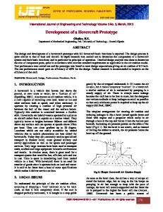
2.1 Single-Pass Resonance Figure 1 is the scheme of the mode-locked laser. It is consists of a VCSEL and a concave external reflecting mirror outside the laser oscillator. The light increases when it shuttles between the laser oscillator and concave external reflecting mirror. Therefore, the light of flickered specific frequency is produced. The repetitive frequency f of the mode-locked laser is represented by c (1) f = 2z where c is the velocity of the light and z is the distance between the VCSEL and concave external reflecting mirror. Supposing that the light is a Gaussian beam, the radius of curvature R of a wave surface is represented by π 2 w04 R( z ) = z + (2) zλ2 where w0 is the diameter of beam west and λ is the laser wavelength. The VCSEL utilized in the experiment consists of the reflecting layer and active region made out of AlGaAs /GaAs pair and it induces the laser light with λ = 985 nm. 外部反射鏡 Concave mirrorR=3.75
VCSEL VCSEL
スペーサ Spacer z
3.5
1.
高周波基板 Circuit board
Figure 1: Scheme of mode-locked VCSEL using concave external reflecting mirror.
P
外部反射鏡 Concave mirror
R
Spacer スペーサ
Figure 2: Scheme of double-pass resonance.
RF power [dBm]
-30
-40
w/o RF f RF = 2.63 GHz V eff = 1.0 V
-50
-60
4.8
5
VCSEL VCSEL
Figure 4: Image of improved mode-locked VCSEL.
O’ O Q
Res: 3 MHz IDC = 6 mA
リング状 位置決めジグ Arraignment ring
5.2 5.4 Frequency [GHz]
5.6
Figure 3: RF spectrum response using double-pass resonance.
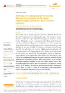
A multilayer film of a dielectric substance is formed depositing SiO2 and Ta2O5 alternatively onto the concave external reflecting mirror. The multilayer film produces the reflecting film with reflectance of 99 percent for light λ = 985 nm. We have realized active mode clock of sub-harmonic by adding high frequency current of 1/integer of mode clock frequency. The high-frequency board is made out of AlN. It supports the VCSEL and spreads heat produced from the VCSEL quickly. The heat-resistant glass was utilized for a spacer in order to prevent a secular change due to outside environment and a deformation due to the change of temperature. 2.2 Double-Pass Resonance We predict that the allowable error between the VCSEL and concave external reflecting mirror is 2.5 μm when single-pass resonance of 40GHz is realized. It is difficult to realize mode clock within this value. Figure 2 shows the scheme of double-pass resonance. A double-pass resonance is realized by the following method. The light emitted from the active layer O' of VCSEL reflects at point P on the concave external reflecting mirror and reflects at point Q on VCSEL except O'. Afterwards, the light returns to the concave external reflecting mirror again, and returns to O' that is after
reflects at R [7]. A mode-locking frequency is determined by the external cavity length, which is close to the distance between the VCSEL and the concave external reflecting mirror. z in Eq. (1) is also twice because optical pass is twice when single-pass replaces resonance as double-pass. The reflectivity of top-DBR of the VCSEL was reduced to expand the bandwidth, where multi-axial modes can be oscillated to achieve mode-locking. Thus, optical confinement in the VCSEL cavity is reduced and the efficient feedback with the concave external reflecting mirror is needed for low threshold current lasing operation. 3. Manufacture of Module by Active Alignment Figure 3 shows the RF spectrum of the module using double-pass resonance. The high speed clock occurs due to sub-harmonic mode clock [8]. The radius of curvature of the concave external reflecting mirror is 14.12 mm and the mode locked frequency is 5.25 GHz. The distance between an external resonator and the reflecting mirror derived from repeatetive clock frequency 14.3 mm. This value is smaller than that obtained from Eq. (2). This means that beam west is at the place away from the surface and the light emitting from the VCSEL converges at once due to any lens effectiveness. The mode clock of 10.5 GHz using single-pass resonance was confirmed. However, synchronous was not realized due to the shrink for fixation of ultraviolet ray hardening resinous. The reason is that tolerance of alignment is beyond due to the shrink of ultraviolet ray hardening. In this structure, the layer of the adhesion for the space of alignment is about 1 mm when the module is manufactured. This means that the amount of the shrink is large. Therefore, the structure which satisfies that the degree of freedom of alignment is high and the influence of the shrink is small is needed. The structure of module with the image as shown in Fig. 4 is proposed in order to secure the space of alignment and to decrease the influence of the shrink. The active alignment is realized through the ring 20 mm larger than outside diameter of the concave external reflecting mirror. A jig for the positioning and fixation of the spacer are realized by the ultraviolet ray hardening. The resin of ultraviolet ray hardening is infused between a jig for the positioning and concave external reflecting mirror after hardening is finished. The
Base plate camera
Collet heater
1mm
20mm
VCSELs
20mm Pulse heater
Wilkinson divider
Die collet
Die camera
Figure 7: Appearance of developed die bonder.
Figure 5: Arrayed VCSEL circuit board.
VCSEL
Arraignment accuracy ±5 μm N2 gus
Die collet with heater AuSn pre form
Pulse heater
AlN circuit board
Figure 6: Function of developed die bonder.
Figure 8: Arrayed module.
fRF=6.53GHz
ultraviolet ray is radiated after alignment is realized again. The fixation is finished after these procedures. The shrink of the resin of the ultraviolet ray hardening has a small influence on alignment in this method. 4.
Array Model of Module Figure 5 shows the arrayed VCSEL circuit board. Wilkinson divider was utilized and diverged to two branches matching impedance to 50 Ω in high frequency board. Since two layers consisting of this structure are utilized, the divider is diverged to four branches. Inputting sub-harmonic signal to one point, the signal is impressed to four resonances simultaneously. This means that load of wiring in alignment is decreased. The interval of the VCSEL is 20 mm and total four VCSELs are united in AuSn pre-form. The VCSEL were bonded using a gold wire. The four VCSELs are allayed in one VCSEL chip. The reason is that the bad for module can be avoided by connecting wire again when the bad of element occurs. It is necessary array VCSEL on the board in order to realize the module of array model. Figure 6 and Fig. 7 show the function and appearance of the developed die bonder, respectively. It is necessary to bond using AuSn alloy in order to avoid to deteriorate the characteristics of high frequency of the VCSEL. In addition, it is necessary to heat locally in order to melt only AuSn not to melt AuSn of the bonded VCSEL. The pulse heater was utilized in order to restrain the damage of element and to prevent the oxidation. The bonding was performed in the
Figure 9: RF spectrum response of arrayed module. atmosphere of N2 gas. Under the situation, the alignment of ±5 μm was realized. Figure 8 shows the allayed module. The module is mounted on the mount made out of copper and the high frequency signal is input. The double-pass resonance was tried using an concave external reflecting mirror with radius of 3.75 mm. Afterwards, the light axis of the mirror is adjusted and the outgoing light was observed using a photodiode. As a result, the resonances of two VCSEL chips through alignment were confirmed. Figure 9 shows RF frequency response of the VCSEL resonance. When the signal of 6.53 GHz is input, the resonance of harmonic oscillation in the neighborhood of 19.6 GHz is confirmed. However, the signal is disappear as well as the case of single-pass resonance when the ultraviolet ray hardening resin is mounted.
Concave mirror
Coplanar line
Input 50 mm Wilkinson divider
Spacer array Fig Arrayed module model.
Figure 10: Structure of allayed module.
19 mm 15 mm
0.12 mm Cut line Input
Figure 11: Divided module model and cut line.
5.
Manufacture Model of Array Module The dummy concave external reflecting mirror and high frequency circuit were tacked after the spacer was glued to this circuit in order to demonstrate this process. Figure 10 shows the structure of allayed module and Fig. 11 shows the divided module and cut line. A cut until 2 mm is provided beforehand in order to decrease cutting resistance. The spacer is glued with accuracy 3 μm based on the mark on the board and the circular mark of φ 100 μm. Each module is cut after active alignment. The Wilkinson divider is removed at this point and four modules are completed. The ingress of water in cutting process and lack by cutting did not occur and therefore cutting was realized normally. As a result, the validity of the manufacturing method of the module was confirmed. 6. Conclusions A high speed optical clock module using a VCSEL and spherical mirror were proposed. As a result, the following conclusions were obtained. (1) A single module, frequency of which is 5.25GHz has been developed successfully. (2) The array structure of mode-locked laser module was proposed and the resonance of the mode-locked
laser was confirmed. (3) The module model was manufactured through a precise lamination and cutting and therefore we enables to manufacture a great amount of modules. (4) The mode-locking sometimes does not occur when the concave external reflecting mirror is glued due to the shrink. The method reducing the influence of shrink was proposed in order to solve this problem. Acknowledgement This work was supported in part by the JST Research “Development of Ultra-High-Frequency Clock Element Using Nano Machining Technology” promoted by JST Innovation Satellite Niigata.” References [1] H.-J. Wei, C. Meng, and Y.-C.Chang, “Wide-ratio broadband SiGe HBT re generative frequency divider enhanced by differential TIA load,” Electron. Lett., 43, 1022-1023 (2007). [2] T. Anan, N. Suzuki, K. Yashiki, K. Fukatsu, H. Hatakeyama, T. Akagawa, K. Tokutome, and M. Tsuji, “High-Speed 1.1-µm-Range InGaAs VCSELs,” in Optical Fiber Communication Conference and Exposition and The National Fiber Optic Engineers Conference, OSA Technical Digest (CD) (Optical Society of America, 2008), paper OThS5. http://www.opticsinfobase.org/abstract.cfm?URI=OFC-2 008-OThS5 [3] U. Fliedler and K. J. Ebeling, “Design of VCSEL’s for feedback insensitive data transmission and external cavity active mode-locking,” J. Selected Topics Quantum Electron., 1, 442-450 (1995). [4] K. Jasim, Q. Zhang, A. V. Nurmikko, E. Ippen, A. Mooradian, G. Carey and W. Ha, “Picosecond pulse generation from passively modelocked vertical cavity diode laser at up to 15 GHz pulse repetition rate,” Electron. Lett., 40, 34-36 (2004). [5] D. Lorenser, D. J. H. C. Maas, H. J. Unold, A.-R. Bellancourt, B. Rudin, E. Gini, D. Ebling, and U. Keller, “50-GHz passively mode-locked surface-emitting semiconductor laser with 100-mW average output power,” IEEE J. Quantum Electron., 42, 838-847 (2006). [6] T. Kato, A. Matsutani, T. Sakaguchi, and K. Kobayashi, “31 GHz sub-harmonic active mode-locked VCSEL with low threshold current,” 14th Microoptics Conference, F-2, Brussels, Belgium, 25-27 Sept. 2008. [7] T. Kato, A. Matsutani, T. Sakaguchi, and K. Kobayashi, “Double-path resonance of a mode-locked VCSEL using a concave mirror,” Joint conference of the Opto-Electronics and Communications Conference, 2008 and the 2008 Australian Conference on Optical Fibre Technology., WeM1, Sydney, Australia, 7-10, July 2008. [8] Tomoyuki Kato, Hiroshi Takanashi, Akihiro Matsutani, Takahiro Sakaguchi, Takashi Miyaguchi, and Kohroh Kobayashi, “Active mode-locked laser module using double-path resonance between VCSEL and concave mirror,” 2009 Optical Society of America (Accepted).