32
IEEE JOURNAL OF SOLID-STATE CIRCUITS, VOL. 45, NO. 1, JANUARY 2010
A 201.4 GOPS 496 mW Real-Time Multi-Object Recognition Processor With Bio-Inspired Neural Perception Engine Joo-Young Kim, Student Member, IEEE, Minsu Kim, Student Member, IEEE, Seungjin Lee, Student Member, IEEE, Jinwook Oh, Student Member, IEEE, Kwanho Kim, Student Member, IEEE, and Hoi-Jun Yoo, Fellow, IEEE
Abstract—A 201.4 GOPS real-time multi-object recognition processor is presented with a three-stage pipelined architecture. Visual perception based multi-object recognition algorithm is applied to give multiple attentions to multiple objects in the input image. For human-like multi-object perception, a neural perception engine is proposed with biologically inspired neural networks and fuzzy logic circuits. In the proposed hardware architecture, three recognition tasks (visual perception, descriptor generation, and object decision) are directly mapped to the neural perception engine, 16 SIMD processors including 128 processing elements, and decision processor, respectively, and executed in the pipeline to maximize throughput of the object recognition. For efficient task pipelining, proposed task/power manager balances the execution times of the three stages based on intelligent workload estimations. In addition, a 118.4 GB/s multi-casting network-on-chip is proposed for communication architecture with incorporating overall 21 IP blocks. For low-power object recognition, workload-aware dynamic power management is performed in chip-level. The 49 mm2 chip is fabricated in a 0.13 m 8-metal CMOS process and contains 3.7M gates and 396 KB on-chip SRAM. It achieves 60 frame/sec multi-object recognition up to 10 different objects for VGA (640 480) video input while dissipating 496 mW at 1.2 V. The obtained 8.2 mJ/frame energy efficiency is 3.2 times higher than the state-of-the-art recognition processor. Index Terms—Multi-casting network-on-chip, multimedia processor, multi-object recognition, neural perception engine, visual perception, workload-aware dynamic power management, threestage pipelined architecture.
I. INTRODUCTION
BJECT recognition is a fundamental technology for intelligent vision applications such as autonomous cruise control, mobile robot vision, and surveillance systems [1]–[5]. Usually, it contains not only pixel based image processing for object feature extraction but also vector database matching for final object decision [6]. For object recognition, first, various scale spaces are generated by a cascaded filtering for input video
O
Manuscript received May 04, 2009; revised July 22, 2009 and September 01, 2009. Current version published December 23, 2009. This paper was approved by Guest Editor Kazutami Arimoto. The authors are with the Department of Electrical Engineering and Computer Science, Korea Advanced Institute of Science and Technology, Daejeon 305701, Korea (e-mail:
[email protected]). Color versions of one or more of the figures in this paper are available online at http://ieeexplore.ieee.org. Digital Object Identifier 10.1109/JSSC.2009.2031768
stream. Then, key-points are extracted among neighbor scale spaces by local maxima/minima search, and each of them is converted to a descriptor vector that describes the magnitude and orientation of it. Last, the final recognition is made by nearest neighbor matching with pre-defined object database that generally includes over ten thousands of object descriptor vectors. Since each stage of the object recognition requires huge amount of computations, its real-time operation is hard to be achieved with a single general purpose CPU [3]. To achieve real-time performance over 20 frame/sec with low power consumption under 1 W, many multi-core based vision processors have been developed [1]–[5]. In massively parallel single instruction multiple data (SIMD) processors [1], [2], hundreds of processing elements (PEs) of are employed to maximize data-level parallelism for per-pixel image operations such as image filtering and histogram. However, their identical operations are not suitable for key-point or object level operations such as descriptor vector generation and database matching. On the other hand, the multi-core processor of [3] exploits coarse-grained PEs and memory-centric network-on-chip (NoC) for task-level parallelism over data-level parallelism; however, it cannot provide enough computing power for real-time object recognition due to its data synchronization overhead. Unlike the previous processors, a NoC based parallel processor [4] adopts a visual attention engine (VAE) [7] to reduce the computational complexity of the object recognition. Motivated from human visual system, the VAE selects meaningful key-points out of the extracted ones to give attentions to them before the main object recognition processing aforementioned. Although it reduces the execution time of the whole object recognition, however, its performance is still limited because its visual attention, object feature extraction and descriptor generation, and database matching are performed in series in time domain due to their unbalanced workloads. In this work, we propose a real-time low-power multi-object recognition processor with a three-stage pipelined architecture. The previous visual attention is enhanced to visual perception to give multiple attentions to multiple objects in the input image. For human-like multi-object perception, neural perception engine is proposed with biologically inspired neural networks and fuzzy logic circuits. In the proposed processor, a three-stage pipelined architecture is proposed to maximize the throughput of object recognition. The mentioned three object recognition tasks are pipelined in frame level and their execution times are balanced based on intelligent workload estimations to improve
0018-9200/$26.00 © 2009 IEEE Authorized licensed use limited to: Korea Advanced Institute of Science and Technology. Downloaded on December 29, 2009 at 00:41 from IEEE Xplore. Restrictions apply.
KIM et al.: A 201.4 GOPS 496 mW REAL-TIME MULTI-OBJECT RECOGNITION PROCESSOR WITH BIO-INSPIRED NEURAL PERCEPTION ENGINE
33
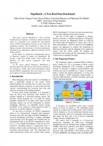
Fig. 1. Visual perception based object recognition model.
pipelining efficiency. In addition, a multi-casting NoC is proposed for the integration of overall 21 IP blocks of the processor. For low power consumption, workload-aware dynamic power management is performed in chip-level. As a result, the proposed processor achieves 60 frame/sec 496 mW multi-object 480) recognition up to 10 different objects for VGA (640 sized video input. The rest of this paper is organized as follows. Section II describes a visual perception based multi-object recognition algorithm in detail. Then, Section III explains system architecture of the proposed processor. Detailed designs of each building block are explained in Section IV. Section V describes the proposed NoC communication architecture. The chip implementation and evaluation results follow in Section VI. Finally, Section VII summarizes the paper. II. VISUAL PERCEPTION BASED MULTI-OBJECT RECOGNITION A. Visual Perception Based Object Recognition Model Fig. 1 shows the concept diagram of the proposed visual perception based multi-object recognition model. The visual perception is an extended mechanism of the previous visual attention [4] to multi-object cases. Based on visual attention, it additionally selects the seed points of the objects and performs seeded region growing to detect the regions-of-interest (ROIs) for objects. Compared with the previous attention, the visual perception gives multiple attentions to multiple objects of the input image by highlighting ROI of each object. After the visual perception, the next object recognition tasks such as key-point extraction and database matching are performed with focusing only on the selected ROIs. By processing only critical regions out of the whole image, computational cost of the object recognition is also reduced in proportional to the area of selected ROIs. B. Overall Algorithm Fig. 2 shows the overall algorithm of the proposed multiobject recognition processor. It is divided into three stages by
the role of each stage: visual perception, descriptor generation, and object decision. This algorithm is devised to recognize around 50 office stuffs in real-time, which is applicable for autonomous mobile robot’s vision system. The visual perception stage is proposed to estimate the ROIs of objects, a global feature of the image, in advance to main object recognition processing. Based on Itti’s visual attention model [8], it extracts not only static features such as intensity, color, and orientation, but also a dynamic feature such as motion vector from the down-scaled input image to generate saliency map. Based on this saliency map, the visual perception selects the seed points of objects and performs seeded region growing to detect ROI of each object [9]. Finally, it determines the ROIs for multiple objects in a unit of 40 40 pixel sized tile, called a grid-tile. For the implementation of visual perception stage, a special hardware block with bio-inspired neural networks and fuzzy logic circuits is proposed to mimic operations of human visual system. The descriptor generation stage extracts key-points of objects out of the selected ROI grid-tiles from the visual perception stage, and generates descriptor vectors for them. To this end, various algorithmic methods such as KLT, Harris-corner detector, affine transformations, and scale invariant feature transform (SIFT) exist [6]. In our algorithm, the SIFT is selected because it is robust to noise injection as well as scale and rotation variances. For the implementation of descriptor generation stage, a parallel processor consisting of many processing units is adopted to tackle parallel and complex image processing tasks. To be applicable for various algorithms, each processing unit is designed as a programmable device. The object decision stage determines the final recognition results by performing database matching for selected regions. It matches the descriptor vectors out of the descriptor generation stage with the object database including thousands of object vectors. A vector matching is to search the minimum distance vector out of the vectors in the database with an input inquiry vector. To accelerate these repeated vector matching operations,
Authorized licensed use limited to: Korea Advanced Institute of Science and Technology. Downloaded on December 29, 2009 at 00:41 from IEEE Xplore. Restrictions apply.
34
IEEE JOURNAL OF SOLID-STATE CIRCUITS, VOL. 45, NO. 1, JANUARY 2010
Fig. 2. Three-stage multi-object recognition algorithm.
dedicated vector distance calculation units are employed in the object decision stage. Overall, the proposed algorithm employs grid-based ROI processing that divides the input image into a number of two-dimensional (2-D) grid-tiles and performs the processing based on them. It enables fine-grained ROI extraction of multiple objects and reduces the effective processing area of input images. To evaluate the proposed algorithm, we perform experiments with 50 office objects out of Columbia object image library (Coil-100) [10]. It is applied to 2400 sample images that include random objects in natural background scenes, with a 16384entry database made by the SIFT. As a result, overall recognition rate by the proposed algorithm is measured as 92%. For evaluations of the ROI detection by visual perception, true positive rate that represents the ratio of correctly detected region out of ground truth ROI and false positive rate that represents the ratio of incorrectly detected region out of not interested region [11] are measured as 70% and 5%, respectively. The visual perception barely affects the overall recognition rate while reducing the processing area of the images to 32.8% on average. III. SYSTEM ARCHITECTURE Fig. 3 shows the overall block diagram of the proposed processor. It consists of 21 IP blocks: a neural perception engine (NPE), a SPU task/power manager (STM), 16 SIMD processor units (SPUs), a decision processor (DP), and two external memory interfaces. The NPE is responsible for the first visual perception stage. It extracts the ROI grid-tiles for each object and sends them to 16 SPUs for detailed image processing. The 16 SPUs, whose power domain is separated into four, are responsible for the second descriptor generation stage. They extract object features out of the selected ROIs and convert
them to descriptor vectors. The descriptor vectors out of the 16 SPUs are gathered at the DP. The DP accelerates the vector matching process of descriptor vectors for the third object decision stage. The STM is specially devised to distribute the tasks of the ROI grid-tiles from the NPE to the 16 SPUs and to manage them. It also controls the pipeline stages of the overall processor and manages four power domains of 16 SPUs. The overall 21 IP blocks are interconnected through the proposed multi-casting NoC. To increase parallelism and hardware utilization of the proposed processor, the proposed three stages are executed in the pipeline in frame level as shown in Fig. 4. The pipelined data are ROI grid-tiles and descriptor vectors between the first–second stage and second–third stage, respectively. Unlike the execution time of the first visual perception stage is constant due to its fixed computation amount, the execution time of the second descriptor generation and third object decision are varying with the number of ROI grid-tiles and descriptor vectors. In order to balance the execution times of three stages, the STM estimates the workload of the following descriptor vector and object decision stage based on the number of extracted ROI grid-tiles and descriptor vectors, respectively, and controls their execution times using two pipeline time balancing schemes. To control the execution time of the descriptor generation stage, the STM performs workload-aware task scheduling (WATS) that differs the number of scheduling SPUs according to the stage’s input workload. Fig. 5(a) shows the flow chart of the WATS. First, the STM measures the number of ROI grid-tiles from the NPE and classifies it to one of N workload levels divided by N-1 threshold values. And then, the STM determines the number of operating SPUs according to the classified workload level. Since it allocates the SPUs in
Authorized licensed use limited to: Korea Advanced Institute of Science and Technology. Downloaded on December 29, 2009 at 00:41 from IEEE Xplore. Restrictions apply.
KIM et al.: A 201.4 GOPS 496 mW REAL-TIME MULTI-OBJECT RECOGNITION PROCESSOR WITH BIO-INSPIRED NEURAL PERCEPTION ENGINE
35
Fig. 3. Overall block diagram of proposed processor.
Fig. 4. Three-stage pipelined architecture.
proportional to the amount of workload, the execution time of the overall descriptor generation stage is kept in constant. The overall execution time is adjusted by modifying threshold values of classification process. By lowering threshold values, the execution time is decreased because more SPUs are assigned for the same amount of workload. On the other hand, the
execution time increases when threshold values become high, while the number of operating SPUs is reduced. To control the execution time of object decision stage, the STM performs applied database size control (ADSC), shown in Fig. 5(b). Based on the vector matching algorithm of the DP [12], the overall execution time of the object decision stage is
Authorized licensed use limited to: Korea Advanced Institute of Science and Technology. Downloaded on December 29, 2009 at 00:41 from IEEE Xplore. Restrictions apply.
36
IEEE JOURNAL OF SOLID-STATE CIRCUITS, VOL. 45, NO. 1, JANUARY 2010
Fig. 5. (a) Workload-aware task scheduling. (b) Applied database size control.
Fig. 6. Block diagram of neural perception engine and SPU task/power manager.
proportional to the number of input descriptor vectors and the size of applied database. Based on these, the execution time of the object decision stage can be controlled by configuring coverage rate of database. First, the STM measures the number of descriptor vectors from the SPUs and calculates the expected execution time of the vector matching. Then, it compares the expected execution time with the target pipeline time and configures the database coverage rate of the DP to meet the pipeline time. However, reducing coverage rate should be carefully performed because it can degrade the overall recognition rate. With a 16384-entry database for 50 objects recognition, correctly matched rate degrades 0.6% and 1.3%, when the coverage rate is 0.95 and 0.90, respectively. With the help of the WATS and ADSC, the execution times of the three stages can be balanced to the target pipeline time, 16 ms, even under
the workload variations. As a result, the proposed processor achieves 60 frame/sec frame-rate for VGA (640 480) sized video input. IV. BUILDING BLOCK DESIGN A. Neural Perception Engine Fig. 6 shows the block diagram of the NPE. For efficient ROI detection, the NPE employs a 32-bit RISC controller and three hardware engines; motion estimator (ME), visual attention engine (VAE), and object detection engine (ODE). The ME is employed to extract dynamic motion vectors between two sequential frames and implemented by array PEs with a full search block matching method [13]. The VAE is employed to extract
Authorized licensed use limited to: Korea Advanced Institute of Science and Technology. Downloaded on December 29, 2009 at 00:41 from IEEE Xplore. Restrictions apply.
KIM et al.: A 201.4 GOPS 496 mW REAL-TIME MULTI-OBJECT RECOGNITION PROCESSOR WITH BIO-INSPIRED NEURAL PERCEPTION ENGINE
37
Fig. 7. Detailed visual perception algorithm.
static features such as intensity, color, and orientation and generate the saliency map that combines the extracted feature maps through repeated normalizations. The ODE is proposed to perform the final ROI classification for each object using the generated saliency map. The RISC controller takes a role in controlling the three dedicated engines and performing software oriented operations between the dedicated operations of the engines. A 24 KB memory is used for storing original images and data communication among the three engines by sharing intermediate processing data. After the final ROI classification, the NPE transfers information of the obtained ROI grid-tiles to the STM through a FIFO queue. Fig. 7 shows the detailed visual perception algorithm operated by the NPE, which broadly consist of saliency map generation and ROI classification. The saliency map generation is mainly based on Itti’s saliency based visual attention [8] and accelerated by the VAE. First, the RGB channels of VGA sized 60 pixels and an inteninput image are down-sized to 80 sity feature map and two color feature maps are generated by per-pixel filtering operations. Four orientation feature maps, for the direction of 0, 45, 90, and 135 , are generated from the intensity feature map with the Gabor filtering. After generating multi-scale Gaussian pyramid images for each of 7 maps, each image is transformed by a center-surround mechanism to enhance the parts of the image that differ from their surroundings. Finally, the saliency map is generated by repeated combination of normalized feature maps. The motion vector map, generated by the ME, is also combined in this step. Among
these processes, computationally intensive image filtering operations such as Gabor, Gaussian, and center-surround filtering are accelerated by the hardware accelerator VAE. The normalization processes, which include irregular operations and can be performed in different ways, are performed by software by the RISC controller. After saliency map generation, ROI classification is performed by the ODE. First, the 10 most salient points are selected as the seed points out of the saliency map. Then, from the most salient seed point, the ROI of an object grows from neighbor pixels of the seed through repeated homogeneity classifications. For the classification of each pixel, an intensity, saliency, and location are used for homogeneity evaluation. The similarities between the seed and target pixel are measured for above three metrics, and based on the summated result, the final classification that the target pixel is determined to be joined to the ROI or not is determined. In case that the other seed points are included by the grown region, they are inhibited from the seed points in the next ROI classification. After repeating classification processes for 10 seed points, the ROI of each object in pixel unit is quantized to the small sized grid-tile unit. In the design of the VAE and ODE, biologically inspired cellular neural networks and neuro-fuzzy classifier are employed for fast feature extraction and robust classification, respectively. In the VAE, 2-D cellular neural networks are used to rapidly extract various features from the input image using its regional and collective processing [7]. Fig. 8 shows overall block diagram, circuits, and measured waveforms of the ODE. It employs Gaussian fuzzy membership and single-layer neural net-
Authorized licensed use limited to: Korea Advanced Institute of Science and Technology. Downloaded on December 29, 2009 at 00:41 from IEEE Xplore. Restrictions apply.
38
IEEE JOURNAL OF SOLID-STATE CIRCUITS, VOL. 45, NO. 1, JANUARY 2010
Fig. 8. Block diagram, circuits, and measured waveforms of object detection engine.
work for similarity measure and decision making, respectively. In circuit design, the ODE exploits analog-based mixed-mode circuits to reduce area and power overhead of Gaussian function circuits and neural synaptic multipliers. Except the digitally implemented learning part, data processing parts of the ODE are implemented by analog circuits. To exploit the analog data processing, 8-bit intensity, saliency, and location values of the target and seed pixel are converted to analog signals by DACs. After that, three Gaussian function circuits measure the similarities between the two pixels for three metrics. A Gaussian function circuit is realized by the combination of MOS differential pair and minimum follower circuit in current mode configuration. The differential pair circuit outputs the symmetric differential signals, each of which has exponential non-linearity characteristics. And the minimum follower circuit generates the Gaussian-like output by following the minimum between the symmetric differential signals. A 2-D Gaussian function circuit can be implemented by two consecutive Gaussian function circuits by connecting the output of a Gaussian function circuit to the bias current input tail of the next Gaussian function circuit. Finally, current-mode neural synaptic circuits merge the three measured similarities with multiplying their weight values, and comparator circuit make the final decision through thresholding. With a Hebbian learning [14], the weight values of the neural synaptic circuits, which play a role in classification criteria, are updated every cycle. As a result, the ODE completes the ROI detection for 1 object within 7 s at 200 MHz operating frequency. And its analog-based mixed-mode implementation reduces the area and power consumption by 59% and 44%, respectively, compared with those of digital implementation.
Fig. 8 also shows the measurement waveforms of mixed-mode ODE. They include DAC output signal, Gaussian function circuit output signal, and final classification signal. As shown in the enlarged waveforms, the Gaussian output signal varies with the similarity of two analog input signals, and the final classification signal is made based on it. B. SIMD Processor Unit The SPU is designed to accelerate parallel image processing tasks of the descriptor generation stage. As shown in Fig. 9, the SPU consist of a SPU controller, eight SIMD controlled dual-issued very long instruction word (VLIW) PEs, 128-bitwide data memory, and 2-D DMA. The eight PEs perform pixel parallel image processing operation such as Gaussian filtering, local maximum search, and histogram operation. The SPU controller controls the overall program flow of the SPU, decodes the instruction for the eight PEs, and performs data transfer between the eight PEs and data memory. For the data memory of the eight PEs, a 128-bit unified memory is used rather than eight 16-bit memories to reduce the area and power consumption by 30.4% and 36.4%, respectively. The two data aligners between the data memory and eight PEs facilitate the data movement by rotating the unified 128-bit data in 16-bit unit. The 2-D DMA performs the data transfer between the external memory and internal data memory in parallel with the PE operation. It automatically generates the addresses for 2-D data access for the data transactions of vision applications. The detailed block diagram of each dual-issued VLIW PE is also shown in Fig. 9. It consists of two independent data
Authorized licensed use limited to: Korea Advanced Institute of Science and Technology. Downloaded on December 29, 2009 at 00:41 from IEEE Xplore. Restrictions apply.
KIM et al.: A 201.4 GOPS 496 mW REAL-TIME MULTI-OBJECT RECOGNITION PROCESSOR WITH BIO-INSPIRED NEURAL PERCEPTION ENGINE
39
Fig. 9. SIMD processor unit and its dual-issued VLIW PE.
paths for data processing operations such as ALU, shift, multiply, and multiply-and-accumulation (MAC), and data transfer operations such as load and store. A 51-bit dual-issued VLIW instruction enables parallel execution of the data processing and data transfer operation for every cycle. Utilizing its own register file with five-read and three-write ports, the PE can execute complex instructions for image processing such as two-way multiply/MAC, three-operanded min/max compare, and 32-bit accumulation in a single cycle. The register files of the other PEs can be directly accessed for window based image processing. In addition, each PE can be conditionally executed for the same instruction using its independently managed status register. C. Decision Processor The object decision stage is composed of repeated vector matching processes that search the nearest vector of each input descriptor among object database. These repeated vector matching can be a performance bottleneck because distance calculations between the input vector and each of thousands of vectors in database require a lot of processing time. In the proposed processor, the DP accelerates the vector matching to make the object decision stage to be operated over 60 frame/sec
frame rate for the database including more than 15,000 vectors. To reduce the search region of database without accuracy loss, the DP exploits the H-VQ algorithm presented in the previous vector matching processor [12]. However, as shown in Fig. 10, the hardware is redesigned to increase the throughput of vector matching with two modifications. First, the H-VQ algorithm is performed with dedicated three-stage pipelined datapath for vector distance calculation and comparison. Second, the bandwidth of database vector memory is increased twice, from 256-bit to 512-bit. For the vector matching operations of the DP, descriptor vectors are gathered in feature vector memory from the SPUs as the first step. Then, the H-VQ algorithm is performed by a controller with the dedicated datapath. Once an input inquiry vector is set, the DP can obtain the index of the minimum distance vector by reading vectors from the database memory because the distance calculations and minimum vector updates are automatically performed in pipelined datapath stages. Since the DP can read two 256-bit vectors from the database memory in a single cycle, the throughput of the DP is two vector distance calculations per cycle at 200 MHz. In overall, the DP matches 256 descriptor vectors with a 16384-entry database within 3M cycles.
Authorized licensed use limited to: Korea Advanced Institute of Science and Technology. Downloaded on December 29, 2009 at 00:41 from IEEE Xplore. Restrictions apply.
40
IEEE JOURNAL OF SOLID-STATE CIRCUITS, VOL. 45, NO. 1, JANUARY 2010
Fig. 10. Block diagram of decision processor.
V. MULTI-CASTING NETWORK-ON-CHIP As the number of IP blocks increases to address computing requirements of recent multimedia processing, conventional shared medium based communication reveals its limitations to handle simultaneous data transactions among multiple IP blocks. As an alternative, a network-on-chip (NoC) is highlighted as suitable communication architecture in multi-core era in spite of its high implementation costs compared with conventional bus, because it provides sufficient bandwidth to multiple IP blocks and has good scalability with distributed router switches [15]–[17]. In this processor, a multi-casting network-on-chip (MC-NoC) is proposed to integrate all of 21 IP blocks. To cope with the processor’s application-driven data transactions such as 1-to-N broad/multi-casting and inter-processor data communications, the MC-NoC has a new combined architecture and supports a multi-casting capability. Fig. 11 shows the proposed MC-NoC architecture that consists of a 9 10 system network and four 7 7 SPU cluster (SPC) networks. The 16 SPUs are connected to the system network through the four SPC networks while the NPE, STM, DP, and two external interfaces are directly connected to the system network. It adopts a hierarchical star topology [15] as a basic topology for low latency data communications, and then, supplements a ring topology to the SPC networks for high-speed inter-SPU data transactions. The additional network links for the combined topology provides 25.6 GB/s aggregated bandwidth between the SPC networks and allows each SPU to access the other SPUs in neighbor clusters in two switch hops. In overall, topology-combined MC-NoC provides a 118.4 GB/s total bandwidth with the switch hop latency of less than 3. The proposed MC-NoC adopts a wormhole routing protocol whose packet is composed of header, address, and data flow control units (FLITs). Each FLIT consists of 2-bit control signals and 34-bit data signals including 2-bit FLIT type indicator. The header FLIT contains all information for the entire packet transmission such as 4-bit burst length for burst data transaction
Fig. 11. Proposed multi-casting NoC architecture.
up to eight FLITs and 2-bit priority level for quality-of-service. The 16-bit source defined routing information (RI) allows four switch traversals for normal packets and multi-casting to arbitrary SPUs for multi-casting packets. In case of multi-casting packets, each bit of 16-bit RI indicates each destination SPU. In the MC-NoC, multi-casting from the NPE/STM to the 16 SPUs is supported to accelerate 1-to-N data transactions such as program kernel distribution and image data download. To this end, each network switch is designed to have multi-casting ability. Fig. 12 shows a four-stage pipelined multi-casting crossbar switch and its multi-casting port. It consists of input ports, arbiters, mux based crossbar fabric, and output ports. At first, the incoming FLITs are buffered at the 8-depth FIFO queue that contains the synchronization interface [18] for heterogeneous clock domain conversion. Then, each active input port sends a request signal to its destination arbiter to get a grant signal to traverse the crossbar fabric. For scheduling of grant signals, the arbiters perform a simple round-robin scheduling according to the priority levels. In case of multi-casting
Authorized licensed use limited to: Korea Advanced Institute of Science and Technology. Downloaded on December 29, 2009 at 00:41 from IEEE Xplore. Restrictions apply.
KIM et al.: A 201.4 GOPS 496 mW REAL-TIME MULTI-OBJECT RECOGNITION PROCESSOR WITH BIO-INSPIRED NEURAL PERCEPTION ENGINE
41
Fig. 12. Four-stage pipelined multi-casting switch and its multi-casting port.
packet, a multi-casting input port sends multiple requests to all destination arbiters at the same time and waits until all grant signals are returned. To this end, in the multi-casting input port, a multi-port requester decodes the 16-bit RI and generates corresponding request signals and a grant checker holds the multi-casting packet until the registered request signals are equal to the received grant signals. After all grants are gathered, multi-casting is performed using the existing broad-casted wires of crossbar fabric without any additional wires. A variable strength driver is specially employed for the multi-casting port to provide sufficient driving strength for multi-casting. As a result, the MC-NoC’s multi-casting capability accelerates the program kernel distribution and image data download task of the target object recognition by 6.56 and 1.22 , respectively. VI. LOW-POWER TECHNIQUES To reduce power consumption during the object recognition processing, chip-level power management is performed by the STM. Fig. 13 shows power management architecture of the proposed processor and its workload-aware dynamic power management. In the chip, power domain of the 16 SPUs is divided into four domains and each of them is independently controlled by the STM. To control the power domains, off-chip power gating method [19] is employed for low cost implementation. An external regulator with enable signal is employed
for each of the power domains. The rest parts of the chip, the NPE, STM, DP and NoC, are placed in always-on domain. For efficient power gating of the chip, workload-aware power gating (WAPG) is adopted with workload-aware task scheduling (WATS). When the STM measures the workload of the SPUs based on the number of ROI grid-tiles and determines the number of activating SPUs, it also determines the number of activated power domains in proportional to the workload amount, as shown in the flow chart of Fig. 13. After that, the STM sends request signals to external regulators to gate unused power domains of SPUs before it assigns the ROI grid-tile tasks to the SPUs. Considering a few hundreds of s settling time of external regulators, the requests for power gating occur only once per frame. By the WAPG, the number of activated power domains adaptively varies according to the workload of input frame as shown in Fig. 13. For further reduction of dynamic power in activated power domains, software controlled clock gating is applied to each operating SPU as shown in Fig. 14. The clock of SPU can be gated by two software requests, end request and wait request. Each request is made by writing operation of the SPU to pre-defined address. The end request occurs when the SPU has finished its assigned task. On the other hand, the wait request is generated in situation that the SPU should stop its operation and wait for other module’s operation. To this end, the SPU writes the index value at the pre-defined wait address to notify the index of wait
Authorized licensed use limited to: Korea Advanced Institute of Science and Technology. Downloaded on December 29, 2009 at 00:41 from IEEE Xplore. Restrictions apply.
42
IEEE JOURNAL OF SOLID-STATE CIRCUITS, VOL. 45, NO. 1, JANUARY 2010
Fig. 13. Workload-aware dynamic power management.
Fig. 15. Chip micrograph.
Fig. 14. Software controlled clock gating.
conditions to be resolved. In this case, the clock is automatically restored when all the wait conditions are resolved. With the WAPG and software controlled clock gating, the power consumption of the 16 SPUs is reduced by 38%, from 542 mW to 336 mW, while the power consumption of the overall processor amounts to 496 mW at 60 frame/sec frame-rate. VII. CHIP IMPLEMENTATION AND EVALUATION The proposed recognition processor is fabricated in a 0.13 m mm chip con1-poly 8-metal CMOS technology and its tains 36.4M transistors including 3.7M logic gates and 396 KB on-chip SRAM. Fig. 15 shows the chip micrograph and Table I summarizes its features. The operating frequency is 200 MHz for IP blocks and 400 MHz for the NoC. Its peak performance amounts to 201.4 giga operations per second (GOPS) when 695 mW is dissipated. Specifically, 128 PEs of 16 SPUs, each of which performs up to five operations per cycle with a two-way MAC instruction, performs 128 GOPS. The NPE performs 54
GOPS; 40 linear PEs of the VAE perform 24 GOPS, four parallel analog-digital mixed datapaths of the ODE perform 20 GOPS, parallel SAD units of the ME perform 9.8 GOPS, and a control RISC performs 0.2 GOPS. The DP performs 19.4 GOPS using its 32 16-bit SAD distance calculation and compare units. The average power consumption of the processor is 496 mW at the supply voltage of 1.2 V while the proposed multi-object recognition is running at 60 frame/sec frame-rate. Table II shows power break-down of the proposed processor. The 16 SPUs account for about two thirds of overall power consumption. Fig. 16 shows performance comparisons of the proposed processor with previous vision processors [2]–[4], [20]. Fig. 16(a) shows power efficiency comparison. The GOPS/W, which normalizes the GOPS performance with the power, is adopted as a performance index where the 1 operation means 16-bit fixed-point operation. The proposed processor achieves 290 GOPS/W, which is 1.36 times higher than the previous vision processors. Fig. 16(b) shows energy efficiency comparison in object recognition, which is obtained by energy consumption per each frame. With 60 frame/sec operation by the pipelined architecture and under 0.5 W power consumption by the workload-aware dynamic power management, the proposed
Authorized licensed use limited to: Korea Advanced Institute of Science and Technology. Downloaded on December 29, 2009 at 00:41 from IEEE Xplore. Restrictions apply.
KIM et al.: A 201.4 GOPS 496 mW REAL-TIME MULTI-OBJECT RECOGNITION PROCESSOR WITH BIO-INSPIRED NEURAL PERCEPTION ENGINE
43
Fig. 16. (a) GOPS/W comparison. (b) Energy/frame comparison.
Fig. 17. Demonstration system.
TABLE I CHIP SUMMARY
TABLE II POWER BREAK-DOWN
processor achieves 8.2 mJ energy dissipation per frame for VGA sized video input, which is 3.2 times lower than the best of the previous object recognition processor. For the validation of the fabricated chip, a demonstration system for real-time object recognition is developed as shown in Fig. 17. It is composed of target objects, video camcorder, evaluation board, and LCD display. The evaluation board is composed of three floors, which are for host processor, video decoder and fabricated recognition chip, and peripheral interfaces such as LCD display, serial, USB, and Ethernet, respectively. In the demonstration system, the fabricated chip is used as a vision processing accelerator while the host processor controls the whole program sequences and accesses peripheral modules to display the results and to interface with the external devices. The overall object recognition is performed by three steps. First, the input image of the target objects is captured from the video camcorder and decoded to three-channel RGB pixel data by the video decoder. Then, the decoded image frame is processed by the proposed multi-object recognition processor. Last, the final recognition results are displayed with the key-points at the LCD screen by the host processor. VIII. CONCLUSION In this work, we have proposed a real-time multi-object recognition processor with a three-stage pipelined architecture. The visual perception based multi-object recognition algorithm has been developed to give multiple attentions to multiple objects in the input image. For human-like multi-object perception, a neural perception engine has been proposed with biologically inspired neural networks and fuzzy logic
Authorized licensed use limited to: Korea Advanced Institute of Science and Technology. Downloaded on December 29, 2009 at 00:41 from IEEE Xplore. Restrictions apply.
44
IEEE JOURNAL OF SOLID-STATE CIRCUITS, VOL. 45, NO. 1, JANUARY 2010
circuits. In hardware architecture, a three-stage pipelined architecture has been proposed to maximize the throughput of recognition processing. The three object recognition tasks are executed in the pipeline and the execution times of the three tasks are balanced for efficient pipelining based on intelligent workload estimations. In addition, a 118.4 GB/s multi-casting network-on-chip has been proposed for communication architecture with incorporating overall 21 IP blocks of the processor. Finally, workload-aware dynamic power management was performed for low-power object recognition. The 49 mm chip contains 3.7M gates and 396 KB on-chip SRAM in a 0.13 m CMOS process. With a demonstration system, the fabricated chip achieves 60 frame/sec multi-object recognition 480) video input up to 10 different objects for VGA (640 while dissipating 496 mW at 1.2 V. The obtained 8.2 mJ/frame energy dissipation is 3.2 times lower than the state-of-the-art recognition processor.
[19] M. Keating et al., Low Power Methodology Manual for System on Chip Design. New York: Springer, 2007. [20] B. Khailany et al., “A programmable 512 GOPS stream processor for signal, image, and video processing,” in IEEE ISSCC Dig. Tech. Papers, Feb. 2007, pp. 272–273.
Joo-Young Kim (S’05) received the B.S. and M.S. degrees in electrical engineering and computer science from the Korea Advanced Institute of Science and Technology (KAIST), Daejeon, Korea, in 2005 and 2007, respectively, and is currently working toward the Ph.D. degree in electrical engineering and computer science at KAIST. Since 2006, he has been involved with the development of the parallel processors for computer vision. Currently, his research interests are parallel architecture, sub-systems, and VLSI implementation for bioinspired vision processor.
Minsu Kim (S’07) received the B.S. and M.S. degrees in electrical engineering and computer science from the Korea Advanced Institute of Science and Technology (KAIST), Daejeon, Korea, in 2007 and 2009, respectively. He is currently working toward the Ph.D. degree in electrical engineering and computer science at KAIST. His research interests include network-on-chip based SoC design and bio-inspired VLSI architecture for intelligent vision processing.
REFERENCES [1] S. Kyo et al., “A 51.2 GOPS scalable video recognition processor for intelligent cruise control based on a linear array of 128 4-way VLIW processing elements,” IEEE J. Solid-State Circuits, vol. 38, no. 11, pp. 1992–2000, Nov. 2003. [2] A. Abbo et al., “XETAL-II: A 107 GOPS, 600 mW massively-parallel processor for video scene analysis,” IEEE J. Solid-State Circuits, vol. 43, no. 1, pp. 192–201, Jan. 2008. [3] D. Kim et al., “An 81.6 GOPS object recognition processor based on NoC and visual image processing memory,” in Proc. IEEE Custom Integrated Circuits Conf. (CICC), Apr. 2007, pp. 443–446. [4] K. Kim et al., “A 125 GOPS 583 mW network-on-chip based parallel processor with bio-inspired visual attention engine,” IEEE J. SolidState Circuits, vol. 44, no. 1, pp. 136–147, Jan. 2009. [5] J.-Y. Kim et al., “A 201.4 GOPS 496 mW real-time multi-object recognition processor with bio-inspired neural perception engine,” in IEEE ISSCC Dig. Tech. Papers, Feb. 2009, pp. 150–151. [6] D. G. Lowe, “Distinctive image features from scale-invariant keypoints,” ACM Int. J. Computer Vision, vol. 60, no. 2, pp. 91–110, Jan. 2004. [7] S. Lee et al., “The brain mimicking visual attention engine: An 80 60 digital cellular neural network for rapid global feature extraction,” in IEEE Symp. VLSI Circuits Dig., Jun. 2008, pp. 26–27. [8] L. Itti et al., “A model of saliency-based visual attention for rapid scene analysis,” IEEE Trans. Pattern Anal. Machine Intell., vol. 20, no. 11, pp. 1254–1259, Nov. 1998. [9] M. Kim et al., “A 22.8 GOPS 2.83 mW neuro-fuzzy object detection engine for fast multi-object recognition,” in IEEE Symp. VLSI Circuits Dig., Jun. 2009, pp. 260–261. [10] S. A. Nene, S. K. Nayar, and H. Murase, Columbia Object Image Library (Coil-100), Columbia University, New York, Technical Report CUCS-006-96, Feb. 1996. [11] S. Agarwal et al., “Learning to detect objects in images via a sparse, part-based representation,” IEEE Trans. Pattern Anal. Machine Intell., vol. 26, no. 11, pp. 1475–1490, Nov. 2004. [12] J.-Y. Kim et al., “A 66 frame/sec 38 mW nearest neighbor matching processor with hierarchical VQ algorithm for real-time object recognition,” in Proc. IEEE A-SSCC, Nov. 2008, pp. 177–180. [13] P. Pirsch, N. Demassieux, and W. Gehrke, “VLSI architectures for video compression—A survey,” Proc. IEEE, vol. 83, no. 2, pp. 220–246, Feb. 1995. [14] D. O. Hebb, The Organization of Behavior. New York: Wiley, 1949. [15] S.-J. Lee et al., “An 800 MHz star-connected on-chip network for application to systems on a chip,” in IEEE ISSCC Dig. Tech. Papers, 2003, pp. 468–489. [16] K. Lee et al., “Low-power networks-on-chip for high-performance SoC design,” IEEE Trans. VLSI Syst., vol. 14, no. 2, pp. 148–160, Feb. 2006. [17] K. Kim et al., “A 76.8 GB/s 46 mW low-latency network-on-chip for real-time object recognition processor,” in Proc. IEEE A-SSCC, Nov. 2009, pp. 177–180. [18] J. N. Seizovic, “Pipeline synchronization,” in Proc. IEEE ASYNC, Nov. 1994, pp. 87–96.
Seungjin Lee (S’06) received the B.S. and M.S. degrees in electrical engineering and computer science from the Korea Advanced Institute of Science and Technology (KAIST), Daejeon, Korea, in 2006 and 2008, respectively. He is currently working toward the Ph.D. degree in electrical engineering and computer science from KAIST. His previous research interests include low-power digital signal processors for digital hearing aids and body area communication. Currently, he is investigating parallel architectures for computer vision pro-
2 cessing.
Jinwook Oh (S’08) received the B.S degree in electrical engineering and computer science from Seoul National University, Seoul, Korea, in 2008. He is currently working toward the M.S. degree in electrical engineering and computer science at KAIST, Daejeon, Korea. His research interests include low-power digital signal processors for computer vision. Recently, he is involved with the VLSI implementation of neural networks and fuzzy logics.
Kwanho Kim (S’04) received the B.S. and M.S degrees in electrical engineering and computer science from the Korea Advanced Institute of Science and Technology (KAIST) in 2004 and 2006, respectively. He is currently working toward the Ph.D. degree in electrical engineering and computer science at KAIST. In 2004, he joined the Semiconductor System Laboratory (SSL) at KAIST as a Research Assistant. His research interests include VLSI design for object recognition, architecture and implementation of NoC-based SoC.
Authorized licensed use limited to: Korea Advanced Institute of Science and Technology. Downloaded on December 29, 2009 at 00:41 from IEEE Xplore. Restrictions apply.
KIM et al.: A 201.4 GOPS 496 mW REAL-TIME MULTI-OBJECT RECOGNITION PROCESSOR WITH BIO-INSPIRED NEURAL PERCEPTION ENGINE
Hoi-Jun Yoo (M’95–SM’04–F’08) graduated from the Electronic Department of Seoul National University, Seoul, Korea, in 1983 and received the M.S. and Ph.D degrees in electrical engineering from the Korea Advanced Institute of Science and Technology (KAIST), Daejeon, in 1985 and 1988, respectively. His Ph.D. work concerned the fabrication process for GaAs vertical optoelectronic integrated circuits. From 1988 to 1990, he was with Bell Communications Research, Red Bank, NJ, where he invented the two-dimensional phase-locked VCSEL array, the front-surface-emitting laser, and the high-speed lateral HBT. In 1991, he became Manager of a DRAM design group at Hyundai Electronics and designed a family of from fast-1M DRAMs and 256M synchronous DRAMs. In 1998 he joined the faculty of the Department of Electrical Engineering at KAIST and now is a full Professor. From 2001 to 2005, he was the Director of the System Integration and IP Authoring Research Center (SIPAC), funded by Korean government to promote worldwide IP authoring and its SOC application. From 2003 to
45
2005, he was the full time Advisor to Minister of Korea Ministry of Information and Communication and National Project Manager for SoC and Computer. In 2007, he founded SDIA (System Design Innovation and Application Research Center) at KAIST to research and develop SoCs for intelligent robots, wearable computers and bio systems. His current interests are high-speed and low-power network on chips, 3-D graphics, body area networks, biomedical devices and circuits, and memory circuits and systems. He is the author of the books DRAM Design (Seoul, Korea: Hongleung, 1996; in Korean), High Performance DRAM (Seoul, Korea: Sigma, 1999; in Korean), and chapters of Networks on Chips (New York: Morgan Kaufmann, 2006). Dr. Yoo received the Electronic Industrial Association of Korea Award for his contribution to DRAM technology the 1994, Hynix Development Award in 1995, the Korea Semiconductor Industry Association Award in 2002, Best Research of KAIST Award in 2007, Design Award of 2001 ASP-DAC, and Outstanding Design Awards 2005, 2006, 2007 A-SSCC. He is a member of the executive committees of ISSCC, Symposium on VLSI, and A-SSCC, and was the TPC chair of the A-SSCC 2008.
Authorized licensed use limited to: Korea Advanced Institute of Science and Technology. Downloaded on December 29, 2009 at 00:41 from IEEE Xplore. Restrictions apply.


![MW]?](https://m.moam.info/img/260x300/mw_5a85191f1723ddfcf8be47bb.jpg)