A COEFFICIENT SEGMENTATION ALGORITHM FOR LOW POWER IMPLEMENTATION OF FIR FILTERS A. T. Erdogan and T. Arslan University of Edinburgh Department of Electronics and Electrical Engineering Edinburgh, EH9 3JL, Scotland, UK.
[email protected]
ABSTRACT The authors present a multiplication algorithm for low power implementation of digital filters on CMOS based digital signal processing systems. The algorithm decomposes individual coefficients into two primitive sub-components. The decomposition, performed using a heuristic approach, divides a given coefficient such that a part is produced which can be implemented using a single shift operation leaving another part with a reduced wordlength to be applied to the coefficient input of the hardware multiplier. This results in a significant reduction in the amount of switched capacitance and consequently power consumption. The algorithm has been used with a number of practical FIR filter examples achieving up to 63% saving in power. Results are provided which illustrate the effect of the algorithm on the amount of switched capacitance for different size multipliers. The paper provides a description of the algorithm, the evaluation procedure used, and associated results including overheads due to shift operations.
[email protected] with reduced wordlength to be applied to the inputs of the hardware multiplier. Hence resulting in a significant reduction in the amount of switched capacitance and consequently power consumption. Two’s complement representation is most commonly used in DSP applications. This is due to ease of performing arithmetic operations such as additions and subtractions. However, a major drawback of two’s complement representation is the sign extension, which causes the MSB sign-bits to switch when signals transition from positive to negative or vice-versa [1], hence increasing its power overhead. For this reason, the proposed algorithm is especially tailored for filters using two’s complement multipliers, although the algorithm can be generalised to filters with multipliers using other data representations such as sign magnitude etc. Begin
H = (h0, h1, … , hL-1)
1. INTRODUCTION
i = 0, k = 0
Due to the surge in portable computing industry, there is a continuous demand for effective methods of implementing commonly used computationally intensive DSP tasks such as digital filtering. It can be shown that the most significant factor affecting power consumption in a CMOS VLSI device is the switching power, which is expressed by the product [(supply voltage)2 x switched capacitance] [1]. In this product, the switched capacitance is a combination of the physical capacitance, C, and the switching activity factor, k, which is defined as the average number of times that a gate makes a logic transition (1→0 or 0→1) in each clock cycle. Therefore, one way of reducing the power consumption of digital filters, is to reduce the amount of switched capacitance during its operation. Example approaches in the literature for reducing the switched capacitance of digital filters are coefficient ordering [2], data block processing [3], dynamically minimising filter order [4], choice of appropriate coding techniques [1,5], and the application of high level transformations [6,7]. This paper presents a new multiplication algorithm for low-power implementation of digital filters on CMOS DSPs. The algorithm reduces the switched capacitance by decomposing individual coefficients into two less complex sub-components. The decomposition, performed using a heuristic approach, separates a given coefficient such that a part is produced which can be implemented using a single shift operation leaving another part
III-359 0-7803-5474-5/99/$10.00(C)1999 IEEE
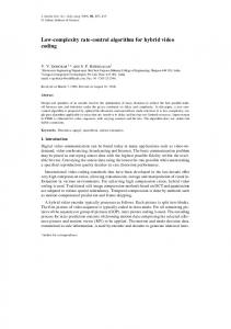
2i >= |hk|
1
No i=i+1
Yes 2i != |hk|
2
No
sk = hk mk = 0
Yes No hk L -1
k=k+1 Yes End
Figure 1. A flow chart of the algorithm
Table 1: Total switching activity of H and M coefficient sets Original coefficient set
8-bit two’s complement binary format in table 1. Clearly, the total switching activity is reduced from 34 to 16 (by 52.94%) in this case. In addition, the effective coefficient wordlength is reduced to six bits since the most significant 2 bits of M are always zero. Given the data samples X = (21, -64, 127, 64, -59, -93, 12, 17, 54, -82, …) then the shift operations and the hardware multiplications produce the following output sets: Ys = (-2688, 7856, -17920, -2704, -10368, 6096, -1264, -16448, -2992, 44224 …), and Ym = (651, -1963, 3894, 2110, -1641, -2548, 564, 2689, 4933, 519, …) respectively. The final filter output is obtained by summing the two sets, i.e. Y = Ys + Ym = (-2037, 5893, -14026, -594, -12009, 3548, -700, -13759, 1941, 44743, …).
Two’s Two’s Decomposed complement complement coefficient set representation representation
h0 = -97
10011111
m0 = 31
00011111
h1 = -15
11110001
m1 = 1
00000001
h2 = -127
10000001
m2 = 1
00000001
h3 = -29
11100011
m3 = 3
00000011
h4 = -119
10001001
m4 = 9
00001001
h5 = -103
10011001
m5 = 25
00011001
h6 = 93
01011101
m6 = 29
00011101
h7 = 57
00111001
m7 = 25
00011001
h8 = -111
10010001
m8 = 17
00010001
h9 = 127
01111111
m9 = 63
00111111
Total Switching
34
Total Switching
16
3. SIMULATIONS AND RESULTS 8x8, 16x16, and 24x24-bit twos complement array multipliers are implemented using Cadence VLSI suite with ES2 0.7µm CMOS technology. Coefficient sets are obtained by designing ten practical FIR filters, five lowpass and five bandpass, for different filter specifications with filter lengths varying from 32 to 89 as shown in tables 2 and 3. The coefficient sets are quantised to 8, 16, and 24-bits. This is followed by generating zero mean
Input Samples
Coefficient Set
2. IMPLEMENTATION The flow chart in Figure 1 illustrates the main stages of the algorithm (indicated in circles). Given the coefficient set H = (h0, h1, …, hL-1), where L is the filter order, the algorithm proceeds through the coefficients sequentially. For a given coefficient hk, the algorithm targets dividing it such that hk = sk + mk, where sk is the component to be implemented using a shift operation and mk is the number to be applied to the hardware multiplier. In order to reduce the switched capacitance of the hardware multiplier consecutive values of mk applied to the multiplier input must be of the same polarity, to minimise switching, and have the smallest value possible, to minimise effective wordlength. In our case mk is chosen to be the smallest positive number. This criteria can be met by careful selection of sk and consequently mk. This selection procedure is the pivot of the stages shown in Figure 1. For a small positive mk, sk must be the largest power of two number closest to hk. For this reason, stage 1 is an iterative procedure which aims to find the largest power of two number greater than or equal to |hk|. Stage 2 deals with coefficients which are already power of two numbers, in which case the complete coefficient is realised using a single shift operation (i.e., sk = hk and mk = 0). In stage 3, the polarity of hk is monitored. If hk is a positive number then sk is chosen as the largest power of two number smaller than hk (i.e., sk = 2i-1). On the other hand if hk is negative, sk is chosen to be the smallest power of two number larger than hk (i.e., sk = -2i ). In both cases mk is hk - sk. As an example, consider a filter with H = (-97, -15, -127, -29, -119, -103, 93, 57, -111, 127). Application of the algorithm will yield the sk values in S = (-128, -16, -128, -32, -128, -128, 64, 32, -128, 64) and the mk values in M = (31, 1, 1, 3, 9, 25, 29, 25, 17, 63). In order to show the reduction in switching activity at the coefficient inputs of the multiplier, hk and mk values are shown in
Simulation Test Vector Generator Test vectors HDL Files
Switching Monitor
Circuit
Switching activity k i
Layout
III-360 0-7803-5474-5/99/$10.00(C)1999 IEEE
Verilog-XL Simulator
Capacitance Ci
M
∑k C i =1
i
i
Total switched capacitance Figure 2. Scheme for evaluating power consumption
Filter #
Passband (kHz)
1 2 3 4 5
0 - 1.5 0 - 1.2 0 - 3.375 0-1 0 - 1.5
Filter #
Stopband (kHz)
1 2 3 4 5
0 - 0.1 0 - 0.45 0 -5 0-1 0 - 0.1
Table 2: Lowpass filter specifications Passband Stopband Stopband ripple attenuation (kHz) (dB) (dB) 2-4 0.1 50 1.7 - 5 0.01 40 5.625 - 10 0.002 90 1.5 - 5 0.0135 56 2-4 0.1 50
Window function
Filter length
Hamming Kaiser Blackman
53 71 42 61 89
Table 3: Bandpass filter specifications Passband Stopband Passband Stopband ripple attenuation (kHz) (kHz) (dB) (dB) 0.15 - 0.25 0.3 - 0.5 0.1 60 0.9 - 1.1 1.55 - 7.5 0.8 30 8 - 12 15 - 44.14 0.00868 60 2 - 3.5 4.25 - 5 0.13 56.4 1.375-3.625 4-5 0.1 68.4
uniformly distributed data samples for each filter. Next the coefficient sets are processed by the algorithm, which produces sk and mk values for each coefficient. This is followed by generating input simulation files, in which the generated input data samples are associated with the corresponding mk values for a given filter, for the Cadence’s Verilog-XLTM digital simulator [8]. VerilogXL uses a hardware description language (Verilog HDL) form of the multiplier circuit for the simulation procedure. For each simulation the number of signal transitions for each gate is monitored. Capacitive information (wiring and loading capacitances) for each gate, Ci, is extracted by performing a layout of the multiplier circuit. Both capacitive information and the switching activity figure, ki, are used to obtain the switched capacitance of each gate. This is then accumulated to give an overall figure for the switched capacitance of the multiplier, see Figure 2. The results obtained with the algorithm are shown in table 4 for different multiplier sizes. For each case, our results are compared to conventional filtering, where data and coefficient values are directly applied to the multiplier inputs. In each case, the results illustrate the amount of switched capacitance per multiplication and the percentage reduction in power when the new algorithm is compared with the conventional approach. Clearly, power saving is achieved in all cases with a maximum of 64.88% when the average of all cases is considered for an 8x8-bit multiplier. In order to estimate the overheads caused by shift operations, high-level models of the multiplier and the shifter circuits are used [7]. Analysis based on these models revealed that an 8-bit shifter consumes 97.67% less capacitance than an 8x8-bit
Filter length
Kaiser Kaiser -
73 34 54 32 80
multiplier. Similarly, 16 and 24-bit shifters consume 98.73% and 99.09% less capacitance than 16x16 and 24x24-bit multipliers respectively. These are used with our simulation results for estimating overheads. For instance, our simulations with an 8x8bit multiplier revealed that using the conventional and the new multiplication algorithms, the average switched capacitance per multiplication is 14.88 pF and 5.23 pF respectively. Hence, the switched capacitance of the shifter is calculated as 14.88 – 14.88*97.67/100 = 0.34 pF. This is added to 5.23 to account for the shifter overhead. For this reason the net reduction for the above multiplier with our algorithm is 62.56%. The above procedure is repeated for both 16x16 and 24x24-bit multipliers, see table 5. These results show that overheads are between 1 and 3%.
4. CONCLUSIONS A power saving algorithm for the implementation of digital filters on CMOS DSP systems is introduced. The algorithm targets reducing the amount of switched capacitance within the multiplier section of the filter, being the most computationally intensive part of the DSP, through fragmentation of the coefficients into two primitive parts, which can be processed with a significant reduction in the amount of switched capacitance. Results are presented, using a range of practical FIR filter examples, which indicate significant power savings. Although the algorithm has been demonstrated with FIR filter examples and two’s complement representation, it can be generalised to most types of digital filter implementations using different data representations.
III-361 0-7803-5474-5/99/$10.00(C)1999 IEEE
Window function
Filter #
Table 4: Power reductions achieved 8-bit 16-bit swcap/mult Reduction swcap/mult Reduction (pF) (%) (pF) (%)
Algorithm
LPF1 LPF2 LPF3 LPF4 LPF5 BPF1 BPF2 BPF3 BPF4 BPF5 AVERAGE
conventional new conventional new conventional new conventional new conventional new conventional new conventional new conventional new conventional new conventional new
15.43 4.86 12.24 4.60 15.60 5.41 16.56 5.36 11.68 4.36 12.75 4.95 16.77 5.59 11.67 5.43 17.16 6.57 18.93 5.13
conventional new
14.88 5.23
72.88
113.81 59.96 104.65 44.66 127.66 50.61 118.43 51.00 103.36 38.34 113.80 43.88 100.45 57.98 98.27 45.14 123.87 58.66 125.72 50.67
64.88
113.00 50.09
68.53 62.40 65.36 67.62 62.71 61.18 66.67 53.49 61.71
24-bit swcap/mult Reduction (pF) (%)
59.69
410.86 252.67 398.56 252.69 445.42 264.96 431.52 261.19 376.95 208.53 400.71 231.08 406.36 299.88 366.24 235.65 456.04 295.68 445.44 260.86
55.67
413.81 256.32
47.31 57.33 60.36 56.94 62.90 61.44 42.28 54.07 52.65
38.50 36.60 40.52 39.47 44.68 42.33 26.20 35.66 35.16 41.44 38.06
Table 5: Average power reductions including overheads Multiplier size 8-bit 16-bit 24-bit
Algorithm
swcap/mult (pF)
conventional new conventional new conventional new
14.88 5.57 113.00 51.52 413.81 260.08
[3] T. Arslan and A.T. Erdogan: “Data Block Processing for Low Power Implementation of Direct Form FIR Filters on Single Multiplier CMOS DSPs”, IEEE ISCAS’98, 31 May – 3 June 1998, Monterey, CA, USA.
Reduction (%)
[4] J.T. Ludwig, S.H. Nawab, and A.P. Chandrakasan: “Low Power Digital Filtering Using Approximate Processing”, IEEE Journal of Solid-State Circuits, vol. 31, no. 3, pp. 395 399, March 1996.
62.56 54.41
[5] C-L. Su, C-Y. Tsui, and A.M. Despain: “Low power architecture design and compilation techniques for high performance processors”, IEEE COMPCON 94, pp. 489498, February 1994.
37.15
5. REFERENCES [1] A.P. Chandrakasan and R.W. Brodersen: “Minimising Power Consumption in Digital CMOS Circuits”, Proceedings of IEEE, Vol. 83, No. 4, April 1995, pp. 498523. [2] A.T. Erdogan and T. Arslan: “Low power multiplication scheme for FIR filter implementation on single multiplier CMOS DSP processors”, IEE Electronic Letters, vol. 32, no. 21, pp. 1959-60, 10th October 1996.
[6] M.S. Bright and T. Arslan: “A Genetic Framework For The High-Level Optimisation Of Low Power VLSI DSP Systems”, IEE Electronics Letters, Vol. 32, No. 13, pp. 1150-1151, 20th June 1996. [7] A.P. Chandrakasan, M. Potkonjak, R. Mehra, J. Rabaey, and R.W. Brodersen: “Optimizing Power Using Transformations”, IEEE Trans. on CAD, Vol. 14, No. 1, January 1995, pp. 12-31. [8] D.E. Thomas and P.R. Morby: “The Verilog Hardware Description Language”, Kluwer Academic Publishers, 1995.
III-362 0-7803-5474-5/99/$10.00(C)1999 IEEE